APT10SCE170B
1700V 10A
Zero Recovery Silicon Carbide Schottky Diode
PRODUCT APPLICATIONS
PRODUCT FEATURES
PRODUCT BENEFITS
• Anti-Parallel Diode
-Switchmode Power Supply
-Inverters
• Zero Recovery Times (trr)
• Higher Reliability Systems
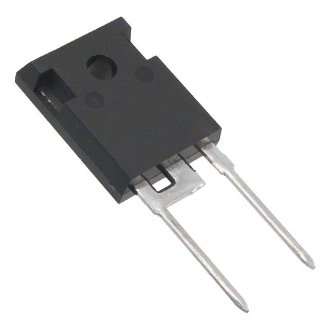
• Popular TO-247 Package
• Power Factor Correction (PFC)
• Low Forward Voltage
• Minimizes or eliminates
snubber
TO
-2 4
7
D 3 PAK
1
2
• Low Leakage Current
1
2
1 - Cathode
2 - Anode
Back of Case - Cathode
MAXIMUM RATINGS
Symbol
VR
All Ratings: TC = 25°C unless otherwise specified.
Characteristic / Test Conditions
Maximum Peak Repetitive Reverse Voltage
VRWM
Maximum Working Peak Reverse Voltage
IFSM
Ptot
TJ, TSTG
TL
Unit
1700
Volts
Maximum D.C. Reverse Voltage
VRRM
IF
Ratings
Maximum D.C. Forward Current
Non-Repetitive Forward Surge Current
( tp = 10ms, Half Sine)
Power Dissipation
TC = 25°C
23
TC = 110°C
15
TC = 25°C
55
TC = 110°C
50
TC = 25°C
214
TC = 110°C
92
Operating and Storage Junction Temperature Range
Amps
W
-55 to 175
Lead Temperature for 10 Seconds
°C
300
STATIC ELECTRICAL CHARACTERISTICS
Characteristic / Test Conditions
Min
Typ
Max
IF = 10A TJ = 25°C
1.5
1.8
IF = 10A, TJ = 175°C
2.25
VF
Forward Voltage
IRM
Maximum Reverse Leakage Current
Qc
Total Capactive Charge VR = 800V, IF = 10A, di/dt = -500A/µs, TJ = 25°C
VR = 1700V TJ = 25°C
10
VR = 1700V, TJ = 175°C
500
Junction Capacitance VR = 0V, TJ = 25°C, f = 1MHz
CT
88
Volts
µA
nC
1120
Junction Capacitance VR = 300V, TJ = 25°C, f = 1MHz
93
Junction Capacitance VR = 600V, TJ = 25°C, f = 1MHz
68
Microsemi Website - http://www.microsemi.com
200
Unit
pF
050-7712 Rev A 3-2014
Symbol
�APT10SCE170B
THERMAL AND MECHANICAL CHARACTERISTICS
Symbol
Characteristic / Test Conditions
RθJC
Junction-to-Case Thermal Resistance
WT
Min
Typ
Package Weight
Torque
Max
Unit
0.7
°C/W
0.22
oz
5.9
g
Maximum Mounting Torque
10
lb·in
1.1
N·m
Microsemi reserves the right to change, without notice, the specifications and information contained herein.
TYPICAL PERFORMANCE CURVES
ZθJC, THERMAL IMPEDANCE (°C/W)
0. 8
0. 7
D = 0.9
0. 6
0.7
0. 5
0. 4
0.5
Note:
0.3
0. 2
t1
t2
0. 1
0
P DM
0. 3
t
Duty Factor D = 1 /t2
Peak T J = P DM x Z θJC + T C
0.1
0.05
SINGLE PULSE
10-3
0.1
1
10
10-2
RECTANGULAR PULSE DURATION (seconds)
FIGURE 1. MAXIMUM EFFECTIVE TRANSIENT THERMAL IMPEDANCE, JUNCTION-TO-CASE vs. PULSE DURATION
10
10
-5
-4
25
20
TJ = -55°C
TJ = 25°C
IF(peak) (A)
IF, FORWARD CURRENT (A)
20
15
10
TJ = 125°C
TJ = 175°C
5
0
10
5
0
1
2
3
4
VF, ANODE-TO-CATHODE VOLTAGE (V)
FIGURE 2, Forward Current vs. Forward Voltage
050-7712 Rev A 3-2014
15
0
25
50
75
100 125 150
175
Case Temperature (°C)
FIGURE 3, Maximum Forward Current vs. Case Temperature
�APT10SCE170B
TYPICAL PERFORMANCE CURVES
350
IR, REVERSE LEAKAGE CURRENT (μA)
250
200
100
50
0
200
150
125°C
100
75°C
50
25°C
200 400 600 800 1000 1200 1400 1600 1800
VR, REVERSE VOLTAGE (V)
Figure 5. Reverse Leakage Currents vs. Reverse Voltage
25
160
0
1200
CJ, JUNCTION CAPACITANCE (pF)
140
120
100
80
60
40
20
0
300
600
900
VR, REVERSE VOLTAGE (V)
Figure 6. Reverse Recovery Charge vs. VR
1000
800
600
400
200
0
1200 1500 1800
0 200 400 600 800 1000 1200 1400 1600 1800
VR, REVERSE VOLTAGE (V)
Figure 7. Junction Capacitance vs. Reverse Voltage
TO-247 Package Outline
4.69 (.185)
5.31 (.209)
1.49 (.059)
2.49 (.098)
15.49 (.610)
16.26 (.640)
6.15 (.242) BSC
5.38 (.212)
6.20 (.244)
20.80 (.819)
21.46 (.845)
Cathode
Qrr, REVERSE RECOVERY CHARGE
(nC)
250
0
50
75
100
125
150
175
CASE TEMPERATURE (°C)
Figure 4. Maximum Power Dissipation vs. Case Temperature
0
300
3.50 (.138)
3.81 (.150)
4.50 (.177) Max .
0.40 (.016)
1.016(.040)
19.81 (.780)
20.32 (.800)
1.65 (.065)
2.13 (.084)
1.01 (.040)
1.40 (.055)
Anode
2.21 (.087)
2.59 (.102)
Cathode
10.90 (.430) BSC
Dimensions in Millimeters and (Inches)
050-7712 Rev A 3-2014
P
(w)
total
150
175°C
�APT10SCE170B
Disclaimer:
050-7712 Rev A 3-2014
The information contained in the document (unless it is publicly available on the Web without access restrictions) is PROPRIETARY AND
CONFIDENTIAL information of Microsemi and cannot be copied, published, uploaded, posted, transmitted, distributed or disclosed or used
without the express duly signed written consent of Microsemi. If the recipient of this document has entered into a disclosure agreement with
Microsemi, then the terms of such Agreement will also apply . This document and the information contained herein may not be modified, by
any person other than authorized personnel of Microsemi. No license under any patent, copyright, trade secret or other intellectual property
right is granted to or conferred upon you by disclosure or delivery of the information, either expressly, by implication, inducement, estoppels or
otherwise. Any license under such intellectual property rights must be approved by Microsemi in writing signed by an officer of Microsemi.
Microsemi reserves the right to change the configuration, functionality and performance of its products at anytime without any notice. This
product has been subject to limited testing and should not be used in conjunction with life-support or other mission-critical equipment or
applications. Microsemi assumes no liability whatsoever, and Microsemi disclaims any express or implied warranty, relating to sale and/or
use of Microsemi products including liability or warranties relating to fitness for a particular purpose, merchantability, or infringement of any
patent, copyright or other intellectual property right. Any performance specifications believed to be reliable but are not verified and customer or
user must conduct and complete all performance and other testing of this product as well as any user or customers final application. User or
customer shall not rely on any data and performance specifications or parameters provided by Microsemi. It is the customer’s and user’s responsibility to independently determine suitability of any Microsemi product and to test and verify the same. The information contained herein
is provided “AS IS, WHERE IS” and with all faults, and the entire risk associated with such information is entirely with the User. Microsemi
specifically disclaims any liability of any kind including for consequential, incidental and punitive damages as well as lost profit. The product is
subject to other terms and conditions which can be located on the web at http://www.microsemi.com/terms-a-conditions.
�