物料型号:
- APT12057B2LL(G)
- APT12057LLL(G)
器件简介:
- Power MOS 7® 是新一代低损耗、高电压、N沟道增强型功率MOSFET。
- 通过显著降低RDS(ON)和Qg,同时降低导通和开关损耗。
- 结合了低导通和开关损耗以及AP Technology专利的金属栅结构所固有的异常快速开关速度。
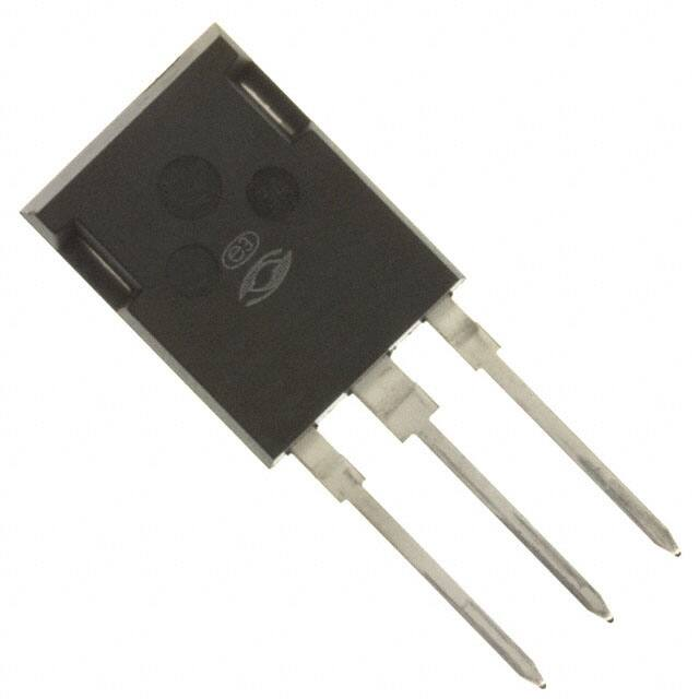
引脚分配:
- D:漏极
- G:栅极
- S:源极
参数特性:
- 最大额定值:
- 漏极-源极电压 (Vpss):1200伏
- 连续漏极电流 (b):22安
- 脉冲漏极电流 ('DM):88安
- 栅极-源极电压 (VGS):±30伏
- 总功率耗散 (P):690瓦
- 工作和存储结温范围 (TJTSTG):-55至150摄氏度
- 静态电气特性:
- 漏极-源极击穿电压 (BVDss):1200伏
- 导通状态漏极电流 (D(on)):22安
- 漏极-源极导通电阻 (RDs(on)):0.570欧姆
- 栅极-源极漏电流 (Gss):±100纳安
- 栅极阈值电压 (GS(th)):3至5伏
功能详解:
- 这些设备对静电放电敏感,应遵循适当的处理程序。
- 提供了动态特性、源-漏二极管的额定值和特性、热特性等详细信息。
应用信息:
- 适用于需要高电压、低损耗和快速开关速度的应用。
封装信息:
- 提供T-MAX™或TO-264封装。
- 封装尺寸信息详细列出,包括引脚间距和最大尺寸。