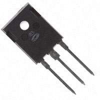
APT50GS60BRDQ2(G) APT50GS60SRDQ2(G)
600V, 50A, VCE(ON) = 2.8V Typical
Thunderbolt® High Speed NPT IGBT with Anti-Parallel 'DQ' Diode
The Thunderbolt HS™ series is based on thin wafer non-punch through (NPT) technology similar to the Thunderbolt® series, but trades higher VCE(ON) for significantly lower turn-on energy Eoff. The low switching losses enable operation at switching frequencies over 100kHz, approaching power MOSFET performance but lower cost. An extremely tight parameter distribution combined with a positive VCE(ON) temperature coefficient make it easy to parallel Thunderbolts HS™ IGBT's. Controlled slew rates result in very good noise and oscillation immunity and low EMI. The short circuit duration rating of 10µs make these IGBT's suitable for motor drive and inverter applications. Reliability is further enhanced by avalanche energy ruggedness. Combi versions are packaged with a high speed, soft recovery DQ series diode.
TO -2 47
D3PAK
Features
• Fast Switching with low EMI • Very Low EOFF for Maximum Efficiency • Short circuit rated • Low Gate Charge • Tight parameter distribution • Easy paralleling • RoHS Compliant
Typical Applications
APT50GS60BRDQ2(G) APT50GS60SRDQ2(G)
• ZVS Phase Shifted and other Full Bridge • Half Bridge • High Power PFC Boost • Welding • Induction heating • High Frequency SMPS Single die IGBT with separate DQ diode die
Absolute Maximum Ratings
Symbol I C1 I C1 I CM VGE SSOA EAS tSC IF I FRM Symbol PD RθJC RθCS TJ, TSTG TL WT Torque Parameter Continuous Collector Current TC = @ 25°C Continuous Collector Current TC = @ 100°C Pulsed Collector Current 1 Gate-Emitter Voltage Switching Safe Operating Area Single Pulse Avalanche Energy 2 Short Circut Withstand Time 3 Diode Continuous Forward Current Diode Max. Repetitive Forward Current Parameter Total Power Dissipation TC = @ 25°C Junction to Case Thermal Resistance Case to Sink Thermal Resistance, Flat Greased Surface Operating and Storage Junction Temperature Range Soldering Temperature for 10 Seconds (1.6mm from case) Package Weight Mounting Torque (TO-247), 6-32 M3 Screw IGBT Diode -55 0.11 0.22 5.9 Min TC = 25°C TC = 100°C Rating 93 50 195 ±30V 195 280 10 90 55 195 Typ Max 415 0.30 0.67 150 300 10 1.1 °C oz g in·lbf N·m
8-2007 052-6300 Rev A
Unit A
V
mJ µs A
Thermal and Mechanical Characteristics
Unit W °C/W
CAUTION: These Devices are Sensitive to Electrostatic Discharge. Proper Handling Procedures Should be Followed.
Microsemi Website - http://www.microsemi.com
�Static Characteristics
Symbol VBR(CES)
∆VBR(CES)/∆TJ
TJ = 25°C unless otherwise specified
Test Conditions VGE = 0V, IC = 250µA
Reference to 25°C, IC = 250µA
APT50GS60B_SRDQ2(G)
Min 600 3 Typ 0.60 2.8 3.25 2.15 1.8 4 6.7 Max 3.15 5 50 TBD ±100 mV/°C µA nA V Unit V V/°C
Parameter Collector-Emitter Breakdown Voltage
Breakdown Voltage Temperature Coeff
VCE(ON) VEC VGE(th)
Collector-Emitter On Voltage 4 Diode Forward Voltage 4 Gate-Emitter Threshold Voltage
VGE = 15V IC = 50A IC = 50A
TJ = 25°C TJ = 125°C TJ = 25°C TJ = 125°C
∆VGE(th)/∆TJ Threshold Voltage Temp Coeff ICES IGES Zero Gate Voltage Collector Current Gate-Emitter Leakage Current
VGE = VCE, IC = 1mA VCE = 600V, VGE = 0V TJ = 25°C TJ = 125°C
VGE = ±20V
Dynamic Characteristics
Symbol gfs Cies Coes Cres Co(cr) Co(er) Qg Qge Ggc td(on) tr td(off) tf Eon1 Eon2 Eoff td(on) tr td(off) tf Eon1 Eon2 Eoff trr
8-2007
Parameter Input Capacitance Output Capacitance
TJ = 25°C unless otherwise specified
Test Conditions VCE = 50V, IC = 50A
Min -
Typ 31 2635 240 145 115 85
Max -
Unit S
Forward Transconductance
Reverse Transfer Capacitance Reverse Transfer Capacitance Charge Related 5 Reverse Transfer Capacitance Current Related 6 Total Gate Charge Gate-Emitter Charge Gate-Collector Charge Turn-On Delay Time Rise Time Turn-Off Delay Time Fall Time Turn-On Switching Energy Turn-On Switching Energy Turn-Off Switching Energy Turn-On Delay Time Rise Time Turn-Off Delay Time Fall Time Turn-On Switching Energy Turn-On Switching Energy
8 9 8 9 10
VGE = 0V, VCE = 25V f = 1MHz
pF
VGE = 0V VCE = 0 to 400V
VGE = 0 to 15V IC = 50A, VCE = 300V
-
235 18 100 16 33 225 37 TBD 1.2 0.755 33 33 250 23 TBD 1.7 0.950 25 35 3
ns nC A mJ ns mJ ns nC
Inductive Switching IGBT and Diode: TJ = 25°C, VCC = 400V, IC = 50A RG = 4.7Ω 7, VGG = 15V
Inductive Switching IGBT and Diode: TJ = 125°C, VCC = 400V, IC = 50A RG = 4.7Ω 7, VGG = 15V
-
Turn-Off Switching Energy 10 Diode Reverse Recovery Time Diode Reverse Recovery Charge Peak Reverse Recovery Current IF = 50A VR = 400V diF/dt = 200A/µs
Qrr Irrm
052-6300
Rev A
�TYPICAL PERFORMANCE CURVES
150 125 100 75
TJ = 25°C
VGE = 15V
250 225
APT50GS60B_SRDQ2(G)
T = 125°C
J
IC, COLLECTOR CURRENT (A)
IC, COLLECTOR CURRENT (A)
200 175 150 125 100 75 50 25 0
V
GE
= 13 & 15V
11V 10V 9V 8V 7V 6V
50 25
TJ = 125°C
TJ = 150°C
0 0 1 2 3 4 5 6 VCE(ON), COLLECTER-TO-EMITTER VOLTAGE (V) FIGURE 1, Output Characteristics
250µs PULSE TEST
很抱歉,暂时无法提供与“APT50GS60BRDQ2G”相匹配的价格&库存,您可以联系我们找货
免费人工找货