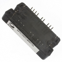
0
登录后你可以
  • 下载海量资料
  • 学习在线课程
  • 观看技术视频
  • 写文章/发帖/加入社区
会员中心
创作中心
发布
  • 发文章

  • 发资料

  • 发帖

  • 提问

  • 发视频

创作活动
APTCV60TLM99T3G

APTCV60TLM99T3G

  • 厂商:

    MICROSEMI(美高森美)

  • 封装:

  • 描述:

    APTCV60TLM99T3G - Three level inverter CoolMOS & Trench Field Stop IGBT Power - Microsemi Corporati...

  • 数据手册
  • 价格&库存
APTCV60TLM99T3G 数据手册
APTCV60TLM99T3G Three level inverter CoolMOS & Trench + Field Stop IGBT Power Module Trench & Field Stop IGBT Q2, Q3: VCES = 600V ; IC = 30A @ Tc = 80°C CoolMOS™ Q1, Q4: VDSS = 600V ; ID = 17A @ Tc = 80°C Application • Solar converter • Uninterruptible Power Supplies Features • Q2, Q3 Trench + Field Stop IGBT Technology - Low voltage drop - Low tail current - Switching frequency up to 20 kHz - Soft recovery parallel diodes - Low diode VF - Low leakage current - RBSOA and SCSOA rated • • • • • Q1, Q4 CoolMOS™ Ultra low RDSon Low Miller capacitance Ultra low gate charge Avalanche energy rated Very rugged Kelvin emitter for easy drive Very low stray inductance High level of integration Internal thermistor for temperature monitoring 28 27 26 25 29 30 23 22 20 19 18 16 15 31 32 2 3 4 7 8 10 11 12 14 13 All multiple inputs and outputs must be shorted together Example: 10/11/12 ; 7/8 … Benefits • Stable temperature behavior • Very rugged • Direct mounting to heatsink (isolated package) • Low junction to case thermal resistance • Easy paralleling due to positive TC of VCEsat • Low profile • RoHS Compliant March, 2009 All ratings @ Tj = 25°C unless otherwise specified These Devices are sensitive to Electrostatic Discharge. Proper Handling Procedures Should Be Followed. See application note APT0502 on www.microsemi.com www.microsemi.com 1-9 APTCV60TLM99T3G – Rev 0 APTCV60TLM99T3G Q1 & Q4 Absolute maximum ratings Symbol VDSS ID IDM VGS RDSon PD IAR EAR EAS Parameter Drain - Source Breakdown Voltage Continuous Drain Current Pulsed Drain current Gate - Source Voltage Drain - Source ON Resistance Maximum Power Dissipation Avalanche current (repetitive and non repetitive) Repetitive Avalanche Energy Single Pulse Avalanche Energy Tc = 25°C Tc = 80°C Max ratings 600 22 17 75 ±20 99 110 11 1.2 800 Unit V A V mΩ W A mJ Tc = 25°C Q1 & Q4 Electrical Characteristics Symbol Characteristic IDSS RDS(on) VGS(th) IGSS Zero Gate Voltage Drain Current Drain – Source on Resistance Gate Threshold Voltage Gate – Source Leakage Current Test Conditions Tj = 25°C VGS = 0V VDS = 600V Tj = 125°C VGS = 10V, ID = 18A VGS = VDS, ID = 1.2 mA VGS = ±20 V, VDS = 0V Min Typ 100 2.5 3 99 3.5 100 Max 50 Unit µA mΩ V nA Q1 & Q4 Dynamic Characteristics Dynamic Characteristics Symbol Characteristic Ciss Input Capacitance Coss Output Capacitance Qg Qgs Qgd Td(on) Tr Td(off) Tf RthJC Total gate Charge Gate – Source Charge Gate – Drain Charge Turn-on Delay Time Rise Time Turn-off Delay Time Fall Time Junction to Case Thermal Resistance Test Conditions VGS = 0V ; VDS = 100V f = 1MHz VGS = 10V VBus = 400V ID = 18A VGS = 10V VBus = 400V ID = 18A RG = 3.3Ω Min Typ 2800 130 14 20 60 10 5 60 5 1.15 °C/W Max Unit pF nC ns Q2 & Q3 Absolute maximum ratings TC = 25°C TC = 80°C TC = 25°C TC = 25°C TJ = 150°C March, 2009 2-9 APTCV60TLM99T3G – Rev 0 Symbol VCES IC ICM VGE PD RBSOA Parameter Collector - Emitter Breakdown Voltage Continuous Collector Current Pulsed Collector Current Gate – Emitter Voltage Maximum Power Dissipation Reverse Bias Safe Operating Area Max ratings 600 50 30 60 ±20 90 60A @ 550V Unit V A V W www.microsemi.com APTCV60TLM99T3G Q2 & Q3 Electrical Characteristics Symbol Characteristic ICES VCE(sat) VGE(th) IGES Zero Gate Voltage Collector Current Collector Emitter Saturation Voltage Gate Threshold Voltage Gate – Emitter Leakage Current Test Conditions VGE = 0V, VCE = 600V Tj = 25°C VGE =15V IC = 30A Tj = 150°C VGE = VCE , IC = 400µA VGE = 20V, VCE = 0V Min Typ 1.5 1.7 5.8 Max 250 1.9 6.5 300 Unit µA V V nA 5.0 Q2 & Q3 Dynamic Characteristics Symbol Characteristic Cies Coes Cres QG Td(on) Tr Td(off) Tf Td(on) Tr Td(off) Tf Eon Eoff Isc RthJC Input Capacitance Output Capacitance Reverse Transfer Capacitance Gate charge Turn-on Delay Time Rise Time Turn-off Delay Time Fall Time Turn-on Delay Time Rise Time Turn-off Delay Time Fall Time Turn-on Switching Energy Turn-off Switching Energy Short Circuit data Junction to Case Thermal Resistance Test Conditions VGE = 0V VCE = 25V f = 1MHz VGE=±15V, IC=30A VCE=300V Inductive Switching (25°C) VGE = ±15V VBus = 300V IC = 30A RG = 10Ω Inductive Switching (150°C) VGE = ±15V VBus = 300V IC = 30A RG = 10Ω Tj = 25°C VGE = ±15V Tj = 150°C VBus = 300V IC = 30A Tj = 25°C RG = 10Ω Tj = 150°C VGE ≤15V ; VBus = 360V tp ≤ 6µs ; Tj = 150°C Min Typ 1600 110 50 0.3 110 45 200 40 120 50 250 60 0.16 0.3 0.7 1.05 150 1.6 ns Max Unit pF µC ns mJ mJ A °C/W www.microsemi.com 3-9 APTCV60TLM99T3G – Rev 0 March, 2009 APTCV60TLM99T3G CR5 & CR6 diode ratings and characteristics Symbol Characteristic VRRM Maximum Peak Repetitive Reverse Voltage IRM IF VF trr Qrr Err RthJC Maximum Reverse Leakage Current DC Forward Current Diode Forward Voltage Reverse Recovery Time Reverse Recovery Charge Reverse Recovery Energy Junction to Case Thermal Resistance IF = 30A IF = 60A IF = 30A IF = 30A VR = 400V IF = 30A VR = 400V Test Conditions VR=600V Tj = 25°C Tj = 125°C Tc = 80°C Min 600 Typ Max 25 500 30 1.8 2.2 1.5 25 160 35 480 0.6 1.2 2.2 V ns nC mJ °C/W Unit V µA A di/dt =200A/µs Tj = 125°C Tj = 25°C Tj = 125°C Tj = 25°C Tj = 125°C Tj = 125°C di/dt =1000A/µs CR2, CR3, CR7 & CR8 diode ratings and characteristics Symbol Characteristic VRRM Maximum Peak Repetitive Reverse Voltage IRM IF VF trr Qrr Err RthJC Maximum Reverse Leakage Current DC Forward Current Diode Forward Voltage Reverse Recovery Time Reverse Recovery Charge Reverse Recovery Energy Junction to Case Thermal Resistance IF = 30A IF = 60A IF = 30A IF = 30A VR = 800V IF = 30A VR = 800V Test Conditions VR=1200V Tj = 25°C Tj = 125°C Tc = 80°C Min 1200 Typ Max 100 500 30 2.6 3.2 1.8 300 380 360 1700 1.6 1.2 3.1 V ns nC mJ °C/W Unit V µA A di/dt =200A/µs Tj = 125°C Tj = 25°C Tj = 125°C Tj = 25°C Tj = 125°C Tj = 125°C di/dt =1000A/µs Temperature sensor NTC (see application note APT0406 on www.microsemi.com for more information). Symbol R25 ∆R25/R25 B25/85 ∆B/B March, 2009 4-9 APTCV60TLM99T3G – Rev 0 Characteristic Resistance @ 25°C T25 = 298.15 K TC=100°C RT = R25 ⎡ ⎛1 1 ⎞⎤ RT: Thermistor value at T exp ⎢ B25 / 85 ⎜ ⎜ T − T ⎟⎥ ⎟ ⎝ 25 ⎠⎦ ⎣ T: Thermistor temperature Min Typ 50 5 3952 4 Max Unit kΩ % K % www.microsemi.com APTCV60TLM99T3G Thermal and package characteristics Symbol VISOL TJ TSTG TC Torque Wt Characteristic RMS Isolation Voltage, any terminal to case t =1 min, I isol
APTCV60TLM99T3G 价格&库存

很抱歉,暂时无法提供与“APTCV60TLM99T3G”相匹配的价格&库存,您可以联系我们找货

免费人工找货