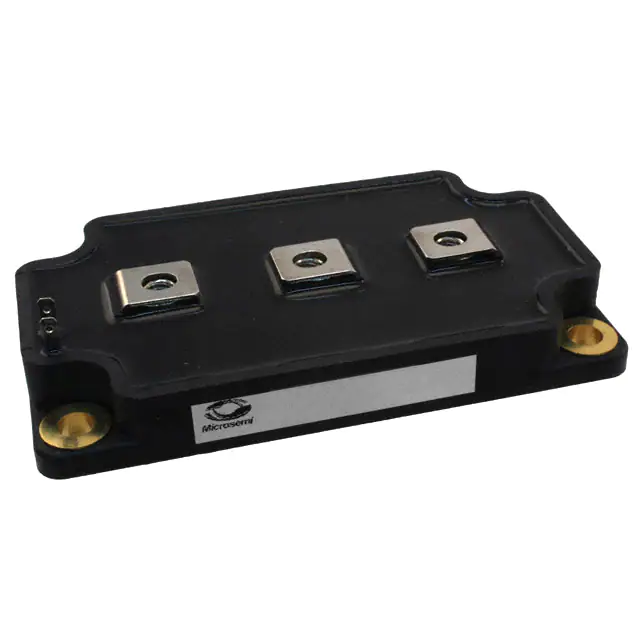
APTGF350DA60G
Boost chopper NPT IGBT Power Module
VBUS
VCES = 600V IC = 350A @ Tc = 80°C
Applicatio n • AC and DC motor control • Switched Mode Power Supplies • Power Factor Correction Features • Non Punch Through (NPT) Fast IGBT® - Low voltage drop - Low tail current - Switching frequency up to 100 kHz - Soft recovery parallel diodes - Low diode VF - Low leakage current - Avalanche energy rated - RBSOA and SCSOA rated • Kelvin emitter for easy drive • Very low stray inductance - Symmetrical design - M5 power connectors • High level of integration Benefits • Outstanding performance at high frequency operation • Stable temperature behavior • Very rugged • Direct mounting to heatsink (isolated package) • Low junction to case thermal resistance • Easy paralleling due to positive TC o f VCEsat • Low profile • RoHS compliant
CR1
OUT
Q2 G2
E2 0/VBUS
VBUS
0/VBUS
OUT
E2 G2
Absolute maximum ratings
Symbol VCES IC ICM VGE PD RBSOA
Parameter Collector - Emitter Breakdown Voltage Continuous Collector Current Pulsed Collector Current Gate – Emitter Voltage Maximum Power Dissipation Tc = 25°C Tc = 80°C Tc = 25°C Tc = 25°C Tj = 150°C
Max ratings 600 430 350 1225 ±20 1562 800A @ 600V
Unit V A V W
July, 2006 1-6 APTGF350DA60G – Rev 2
Reverse Bias Safe Operating Area
These Devices are sensitive to Electrostatic Discharge. Proper Handing Procedures Should Be Followed. See application note APT0502 on www.microsemi.com
www.microsemi.com
�APTGF350DA60G
All ratings @ Tj = 25°C unless otherwise specified Electrical Characteristics
Symbol Characteristic ICES VCE(sat) VGE(th) IGES Symbol Cies Coes Cres Qg Qge Qgc Td(on) Tr Td(off) Tf Td(on) Tr Td(off) Tf Eon Eoff Zero Gate Voltage Collector Current Collector Emitter saturation Voltage Gate Threshold Voltage Gate – Emitter Leakage Current Characteristic Input Capacitance Output Capacitance Reverse Transfer Capacitance Total gate Charge Gate – Emitter Charge Gate – Collector Charge Turn-on Delay Time Rise Time Turn-off Delay Time Fall Time Turn-on Delay Time Rise Time Turn-off Delay Time Fall Time Turn-on Switching Energy Turn-off Switching Energy Test Conditions Tj = 25°C VGE = 0 V VCE = 600V Tj = 125°C Tj = 25°C VGE =15V IC = 360A Tj = 125°C VGE = VCE, IC = 4 mA VGE = ±20V, VCE = 0 V Test Conditions VGE = 0 V VCE = 25V f = 1MHz VGE = 15V VBus = 300V IC = 360A Inductive Switching (25°C) VGE = 15V VBus = 400V IC = 360A R G = 1.25Ω Inductive Switching (125°C) VGE = 15V VBus = 400V IC = 360A R G = 1.25Ω VGE = 15V Tj = 125°C VBus = 400V IC = 360A Tj = 125°C R G = 1.25Ω Test Conditions Tj = 25°C Tj = 125°C Tc = 80°C IF = 400A IF = 800A IF = 400A IF = 400A VR = 400V di/dt =800A/µs 400 1.6 1.9 1.4 180 220 1560 5800 Min 600 VR=600V 750 1500 1.8 V
July, 2006 2-6 APTGF350DA60G – Rev 2
Min
Typ
2.0 2.2 3
Max 200 1750 2.5 5 ±300
Unit µA V V nA Unit nF
Dynamic Characteristics
Min
Typ 17.2 1.88 1.6 1320 1160 800 26 25 150 30 26 25 170 40 17.2 14
Max
nC
ns
ns
mJ
Chopper diode ratings and characteristics
Symbol Characteristic VRRM IRM IF VF
Maximum Peak Repetitive Reverse Voltage
Typ
Max
Unit V µA A
Maximum Reverse Leakage Current DC Forward Current Diode Forward Voltage
Tj = 125°C Tj = 25°C Tj = 125°C Tj = 25°C Tj = 125°C
trr Qrr
Reverse Recovery Time Reverse Recovery Charge
ns nC
www.microsemi.com
�APTGF350DA60G
Thermal and package characteristics
Symbol Characteristic RthJC VISOL TJ TSTG TC Torque Wt Junction to Case Thermal Resistance Operating junction temperature range Storage Temperature Range Operating Case Temperature Mounting torque Package Weight To heatsink For terminals M6 M5 IGBT Diode 2500 -40 -40 -40 3 2 Min Typ Max 0.08 0.16 150 125 100 5 3.5 280 Unit °C/W V °C N.m g
RMS Isolation Voltage, any terminal to case t =1 min, I isol
很抱歉,暂时无法提供与“APTGF350DA60G”相匹配的价格&库存,您可以联系我们找货
免费人工找货