2N6804
Qualified Levels:
JAN, JANTX, and
JANTXV
P-CHANNEL MOSFET
Available on
commercial
versions
Qualified per MIL-PRF-19500/562
DESCRIPTION
This 2N6804 switching transistor is military qualified up to the JANTXV level for high-reliability
applications. Microsemi also offers numerous other transistor products to meet higher and
lower power ratings with various switching speed requirements in both through-hole and
surface-mount packages.
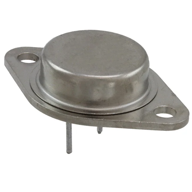
TO-204AA (TO-3)
Package
Important: For the latest information, visit our website http://www.microsemi.com.
FEATURES
•
JEDEC registered 2N6804 number series.
•
JAN, JANTX, and JANTXV qualifications are available per MIL-PRF-19500/562.
•
RoHS compliant version available (commercial grade only).
(See part nomenclature for all available options.)
APPLICATIONS / BENEFITS
•
•
Low-profile metal can design.
Military and other high-reliability applications.
MAXIMUM RATINGS @ T A = +25 ºC unless otherwise stated
Parameters / Test Conditions
Operating & Storage Junction Temperature Range
Thermal Resistance Junction-to-Case
Total Power Dissipation
@ T A = +25 °C
@ T C = +25 °C
Drain-Source Voltage, dc
Gate-Source Voltage, dc
(2)
Drain Current, dc @ T C = +25 ºC
(2)
Drain Current, dc @ T C = +100 ºC
(3)
Off-State Current (Peak Total Value)
Source Current
NOTES:
1.
2.
3.
(1)
Symbol
Value
T J & T stg
R ӨJC
V DS
V GS
I D1
I D2
I DM
-55 to +150
1.67
4
75
-100
± 20
-11.0
-7.0
-50
IS
-11
PT
Unit
o
°C
C/W
W
V
V
A
A
Ω
A
Derated linearly by 0.6 W/ºC for T C > +25 ºC.
The following formula derives the maximum theoretical I D limit. I D is limited by package and internal
wires and may be limited by pin diameter:
MSC – Lawrence
6 Lake Street,
Lawrence, MA 01841
Tel: 1-800-446-1158 or
(978) 620-2600
Fax: (978) 689-0803
MSC – Ireland
Gort Road Business Park,
Ennis, Co. Clare, Ireland
Tel: +353 (0) 65 6840044
Fax: +353 (0) 65 6822298
I DM = 4 x I D1 as calculated in note 2.
Website:
www.microsemi.com
T4-LDS-0113, Rev. 3 (121514)
©2012 Microsemi Corporation
Page 1 of 7
�2N6804
MECHANICAL and PACKAGING
•
•
•
•
•
CASE: TO-3 metal can.
TERMINALS: Solder dipped (Sn63/Pb37) over nickel plated alloy 52. RoHS compliant matte-tin plating is also available.
MARKING: Manufacturer’s ID, part number, date code, ESD symbol.
WEIGHT: Approximately 12.7 grams.
See Package Dimensions on last page.
PART NOMENCLATURE
JAN
2N6804
(e3)
Reliability Level
JAN = JAN Level
JANTX = JANTX Level
JANTXV = JANTXV Level
Blank = Commercial
RoHS Compliance
e3 = RoHS compliant (available
on commercial grade only)
Blank = non-RoHS compliant
JEDEC type number
(see Electrical Characteristics
table)
Symbol
di/dt
IF
RG
V DD
V DS
V GS
SYMBOLS & DEFINITIONS
Definition
Rate of change of diode current while in reverse-recovery mode, recorded as maximum value.
Forward current
Gate drive impedance
Drain supply voltage
Drain source voltage, dc
Gate source voltage, dc
T4-LDS-0113, Rev. 3 (121514)
©2012 Microsemi Corporation
Page 2 of 7
�2N6804
ELECTRICAL CHARACTERISTICS @ T A = +25 °C, unless otherwise noted
Parameters / Test Conditions
OFF CHARACTERISTICS
Drain-Source Breakdown Voltage
V GS = 0 V, I D = -1.0 mA
Gate-Source Voltage (Threshold)
V DS ≥ V GS , I D = -0.25 mA
V DS ≥ V GS , I D = -0.25 mA, T J = +125 °C
V DS ≥ V GS , I D = -0.25 mA, T J = -55 °C
Gate Current
V GS = ± 20 V, V DS = 0 V
V GS = ± 20 V, V DS = 0 V, T J = +125 °C
Symbol
Min.
V (BR)DSS
-100
V GS(th)1
V GS(th)2
V GS(th)3
-2.0
-1.0
Max.
Unit
V
-4.0
V
-5.0
I GSS1
I GSS2
±100
±200
nA
Drain Current
V GS = 0 V, V DS = -80 V
I DSS1
-25
µA
Drain Current
V GS = 0 V, V DS = -80 V, T J = +125 °C
I DSS2
0.25
mA
r DS(on)1
0.30
Ω
r DS(on)2
0.36
Ω
r DS(on)3
0.55
V SD
-4.7
V
Max.
Unit
Q g(on)
29.0
nC
Q gs
7.1
nC
Q gd
21.0
nC
Static Drain-Source On-State Resistance
V GS = -10 V, I D = -7 A pulsed
Static Drain-Source On-State Resistance
V GS = -10 V, I D = -11 A pulsed
Static Drain-Source On-State Resistance
T J = +125°C
V GS = -10 V, I D = -7 A pulsed
Diode Forward Voltage
V GS = 0 V, I S = -11.0 A pulsed
Ω
DYNAMIC CHARACTERISTICS
Parameters / Test Conditions
Gate Charge:
On-State Gate Charge
V GS = -10 V, I D = -11 A, V DS = -50 V
Gate to Source Charge
V GS = -10 V, I D = -11 A, V DS = -50 V
Gate to Drain Charge
V GS = -10 V, I D = -11 A, V DS = -50 V
T4-LDS-0113, Rev. 3 (121514)
©2012 Microsemi Corporation
Symbol
Min.
Page 3 of 7
�2N6804
ELECTRICAL CHARACTERISTICS @ T A = +25 °C, unless otherwise noted (continued)
SWITCHING CHARACTERISTICS
Parameters / Test Conditions
Symbol
Min.
Max.
Unit
Turn-on delay time
I D = -11 A, V GS = -10 V, R G = 7.5 Ω, V DD = -35 V
t d(on)
60
ns
Rinse time
I D = -11 A, V GS = -10 V, R G = 7.5 Ω, V DD = -35 V
tr
140
ns
Turn-off delay time
I D = -11 A, V GS = -10 V, R G = 7.5 Ω, V DD = -35 V
t d(off)
140
ns
Fall time
I D = -11 A, V GS = -10 V, R G = 7.5 Ω, V DD = -35 V
tf
140
ns
Diode Reverse Recovery Time
di/dt ≤ 100 A/µs, V DD ≤ -50 V, I F = -11 A
t rr
250
ns
T4-LDS-0113, Rev. 3 (121514)
©2012 Microsemi Corporation
Page 4 of 7
�2N6804
Thermal Response (ZӨJC)
GRAPHS
t 1 , Rectangle Pulse Duration (seconds)
ID DRAIN CURRENT (AMPERES)
FIGURE 1
Transient Thermal impedance
T C , CASE TEMPERATURE (°C)
FIGURE 2
Maximum Drain Current vs Case Temperature
T4-LDS-0113, Rev. 3 (121514)
©2012 Microsemi Corporation
Page 5 of 7
�2N6804
ID DRAIN CURRENT (AMPERES)
GRAPHS (continued)
V DS , DRAIN-TO-SOURCE VOLTAGE (VOLTS)
FIGURE 3
Safe Operating Area
T4-LDS-0113, Rev. 3 (121514)
©2012 Microsemi Corporation
Page 6 of 7
�2N6804
PACKAGE DIMENSIONS
NOTE:
INCHES
DIM
1. Dimensions are in inches.
MIN
MAX
2. Millimeters are given for general information only.
A
.875
3. These dimensions should be measured at points .050
B
.060
.135
inch (1.27 mm) and .055 inch (1.40 mm) below
C
.250
.360
seating plane. When gauge is not used measurement
D
.312
.500
will be made at the seating plane.
D2
.050
4. The seating plane of the header shall be flat within
E
.038
.043
.001 inch (0.03 mm) concave to .004 inch (0.10 mm)
F
.131
.188
G
1.177
1.197
convex inside a .930 inch (23.62 mm) diameter circle
H
.655
.675
on the center of the header and flat within .001 inch
J
.205
.225
(0.03 mm) concave to .006 inch (0.15 mm) convex
K
.420
.440
overall.
L
.495
.525
5. Mounting holes shall be deburred on the seating
M
.151
.161
plane side.
6. Drain is electrically connected to the case.
7. In accordance with ASME Y14.5M, diameters are equivalent to Φx symbology.
MILLIMETERS
MIN
MAX
22.23
1.52
3.43
6.35
9.15
7.92
12.70
1.27
0.97
1.10
3.33
4.78
29.90
30.40
16.64
17.15
5.21
5.72
10.67
11.18
12.57
13.34
3.84
4.09
NOTES
3
DIA.
Radius
3
3
Radius
DIA.
SCHEMATIC
T4-LDS-0113, Rev. 3 (121514)
©2012 Microsemi Corporation
Page 7 of 7
�