™
Le75183
A
Voice Solution
APPLICATIONS
Line Card Access Switch
VE750 Series
Central office
DLC
PBX
DAML
HFC/FITL
FEATURES
Small size/surface-mount packaging
5-V only operation, very low power consumption
Monolithic IC reliability
DESCRIPTION
The VoiceEdge™ family VE750 series of Line Card Access
Switches (LCAS), which includes the Le75181, Le75282 and
Le75183 devices, is a family of monolithic solid-state switches
that is designed to provide both power ringing access and test
access on the analog line card. These devices, while not a pinfor-pin replacement for the traditional electromechanical relay
(EMR) solution, provide the equivalent switching functionality.
The VE750 series of LCAS is meant as a solid-state alternative
to the EMRs.
The Le75183A/B/C/D devices are pin-for-pin compatible with
Legerity’s L7583A/B/C/D devices.
Clean, bounce-free switching
Legerity also offers a range of compatible SLIC devices and
codec/filters that can be used with the VE750 series LCAS for
complete line card solutions that can be used worldwide in
analog line card applications.
Low, matched ON-resistance
ORDERING INFORMATION
Low impulse noise
Make-before-break, break-before-make operation
Built-in current limiting, thermal shutdown, and SLIC
protection
Battery monitor, all OFF state upon loss of battery
Package Type1
Device
Packing2
Le75183ADSC
Le75183BDSC
Le75183CDSC
No EMI
Le75183DDSC
Latched logic level inputs, no drive circuitry
LE75183AFQC
Only one external protector required
Le75183BFQC
TTL logic control compatible
Le75183CFQC
Default power up state
Le75183DFQC
20-Pin SOIC (GULL)
Tube
32-Pin QFN
Tray
28-pin SOIC (GULL)
Tube
Le75183AFSC
RELATED LITERATURE
081123 Le75282 Dual Intelligent Line Card Access
Switch Data Sheet
081105 Le75181 Ringing Access Switch Data Sheet
080754 Le58QL061/063 QLSLAC Data Sheet
Le75183BFSC
Le75183CFSC
Le75183CZFSC
Le75183DFSC
1.
The green package meets RoHS Directive 2002/95/EC of the
European Council to minimize the environmental impact of
electrical equipment.
2.
For delivery using a tape and reel packing system, add a "T" suffix
to the OPN (Ordering Part Number) when placing an order.
080676 Le5711 Dual SLIC Data Sheet
081047 Le5712 Dual SLIC Data Sheet
NOTE: On August 3, 2007, Zarlink Semiconductor acquired the products and
technology of Legerity Holdings.
Document ID# 081105 Date:
Rev:
C
Version:
Distribution:
Public Document
Sep 18, 2007
2
�Le75183
Data Sheet
TABLE OF CONTENTS
Applications . . . . . . . . . . . . . . . . . . . . . . . . . . . . . . . . . . . . . . . . . . . . . . . . . . . . . . . . . . . . . . . . . . . . . . .1
Features . . . . . . . . . . . . . . . . . . . . . . . . . . . . . . . . . . . . . . . . . . . . . . . . . . . . . . . . . . . . . . . . . . . . . . . . . .1
Related literature . . . . . . . . . . . . . . . . . . . . . . . . . . . . . . . . . . . . . . . . . . . . . . . . . . . . . . . . . . . . . . . . . . .1
Ordering Information . . . . . . . . . . . . . . . . . . . . . . . . . . . . . . . . . . . . . . . . . . . . . . . . . . . . . . . . . . . . . . .1
Description. . . . . . . . . . . . . . . . . . . . . . . . . . . . . . . . . . . . . . . . . . . . . . . . . . . . . . . . . . . . . . . . . . . . . . . .1
Product Description . . . . . . . . . . . . . . . . . . . . . . . . . . . . . . . . . . . . . . . . . . . . . . . . . . . . . . . . . . . . . . . .3
Block Diagrams . . . . . . . . . . . . . . . . . . . . . . . . . . . . . . . . . . . . . . . . . . . . . . . . . . . . . . . . . . . . . . . . . . . .4
Connection Diagrams . . . . . . . . . . . . . . . . . . . . . . . . . . . . . . . . . . . . . . . . . . . . . . . . . . . . . . . . . . . . . .5
Pin Descriptions . . . . . . . . . . . . . . . . . . . . . . . . . . . . . . . . . . . . . . . . . . . . . . . . . . . . . . . . . . . . . . . .6
Absolute Maximum Ratings . . . . . . . . . . . . . . . . . . . . . . . . . . . . . . . . . . . . . . . . . . . . . . . . . . . . . . . . . .7
Operating Ranges . . . . . . . . . . . . . . . . . . . . . . . . . . . . . . . . . . . . . . . . . . . . . . . . . . . . . . . . . . . . . . . . . .7
Environmental Ranges . . . . . . . . . . . . . . . . . . . . . . . . . . . . . . . . . . . . . . . . . . . . . . . . . . . . . . . . . .7
Electrical Ranges . . . . . . . . . . . . . . . . . . . . . . . . . . . . . . . . . . . . . . . . . . . . . . . . . . . . . . . . . . . . . .7
Handling Precautions. . . . . . . . . . . . . . . . . . . . . . . . . . . . . . . . . . . . . . . . . . . . . . . . . . . . . . . . . . . .7
Electrical Characteristics . . . . . . . . . . . . . . . . . . . . . . . . . . . . . . . . . . . . . . . . . . . . . . . . . . . . . . . . . . . .8
Summary of Assumptions . . . . . . . . . . . . . . . . . . . . . . . . . . . . . . . . . . . . . . . . . . . . . . . . . . . . . . . .8
Supply Currents and Power Dissipation . . . . . . . . . . . . . . . . . . . . . . . . . . . . . . . . . . . . . . . . . . . . .8
Specifications . . . . . . . . . . . . . . . . . . . . . . . . . . . . . . . . . . . . . . . . . . . . . . . . . . . . . . . . . . . . . . . . . . . . .8
Device Specifications . . . . . . . . . . . . . . . . . . . . . . . . . . . . . . . . . . . . . . . . . . . . . . . . . . . . . . . . . . .8
Zero Cross Current Turn Off . . . . . . . . . . . . . . . . . . . . . . . . . . . . . . . . . . . . . . . . . . . . . . . . . . . . . . . .13
Switching Behavior . . . . . . . . . . . . . . . . . . . . . . . . . . . . . . . . . . . . . . . . . . . . . . . . . . . . . . . . . . . . . . . .13
Power Supplies . . . . . . . . . . . . . . . . . . . . . . . . . . . . . . . . . . . . . . . . . . . . . . . . . . . . . . . . . . . . . . . . . . .14
Loss of Battery Voltage . . . . . . . . . . . . . . . . . . . . . . . . . . . . . . . . . . . . . . . . . . . . . . . . . . . . . . . . . . . .14
Impulse Noise . . . . . . . . . . . . . . . . . . . . . . . . . . . . . . . . . . . . . . . . . . . . . . . . . . . . . . . . . . . . . . . . . . . .15
Protection. . . . . . . . . . . . . . . . . . . . . . . . . . . . . . . . . . . . . . . . . . . . . . . . . . . . . . . . . . . . . . . . . . . . . . . .15
Integrated SLIC Device Protection . . . . . . . . . . . . . . . . . . . . . . . . . . . . . . . . . . . . . . . . . . . . . . . .15
Typical Performance Characteristics . . . . . . . . . . . . . . . . . . . . . . . . . . . . . . . . . . . . . . . . . . . . . . . . .17
Application . . . . . . . . . . . . . . . . . . . . . . . . . . . . . . . . . . . . . . . . . . . . . . . . . . . . . . . . . . . . . . . . . . . . . . .19
Physical Dimensions. . . . . . . . . . . . . . . . . . . . . . . . . . . . . . . . . . . . . . . . . . . . . . . . . . . . . . . . . . . . . . .22
28-Pin, Plastic SOIC (GULL) (Le75183AESC/BESC/CESC/CZESC/DESC) . . . . . . . . . . . . . . . .22
20-Pin, Plastic SOIC (GULL) (Le75183ASC/BSC/CSC/DSC) . . . . . . . . . . . . . . . . . . . . . . . . . . . .23
32-Pin QFN (Le75183QC/BEQC/CQC/DQC) . . . . . . . . . . . . . . . . . . . . . . . . . . . . . . . . . . . . . . . .24
Revision history. . . . . . . . . . . . . . . . . . . . . . . . . . . . . . . . . . . . . . . . . . . . . . . . . . . . . . . . . . . . . . . . . . .25
Revision A1 to B1 . . . . . . . . . . . . . . . . . . . . . . . . . . . . . . . . . . . . . . . . . . . . . . . . . . . . . . . . . . . . .25
Revision B1 to C1 . . . . . . . . . . . . . . . . . . . . . . . . . . . . . . . . . . . . . . . . . . . . . . . . . . . . . . . . . . . . .25
Revision C1 to C2 . . . . . . . . . . . . . . . . . . . . . . . . . . . . . . . . . . . . . . . . . . . . . . . . . . . . . . . . . . . . .25
2
Zarlink Semiconductor Inc.
�Le75183
Data Sheet
PRODUCT DESCRIPTION
The Le75183A/B/C/D Line Card Access Switch is a monolithic solid-state device providing the equivalent switching functionality
of three 2 form C switches. The Le75183 is designed to provide power ringing access, line test access (test out), and SLIC test
access (test in) to tip and ring in central office, digital loop carrier, private branch exchange, digitally added main line, and hybrid
fiber coax/fiber-in-the-loop analog line card applications. An additional pair of solid-state contacts are also available to provide
access for testing of the ringing generator.
The Le75183A/B has seven states: the idle talk state (line break switches closed, all other switches open), the power ringing state
(ringing access switches closed, all other switches open), loop access (test out) state (loop access (test out) switches closed, all
other switches open), SLIC test state (test in switches closed, all other switches open), simultaneous loop and SLIC access state
(loop and test in switches closed, all others open), ringing generator test state (ring test switches closed, all others open), and
an all OFF state. The seven states in the Le75183A/B are also in the Le75183C/D, with an additional simultaneous test-out and
ring-test state, making the Le75183C/D appropriate for digital loop carrier and other Telcordia TR-57 applications.
The Le75183 offers break-before-make or make-before-break switching, with simple logic level input control. Because of the
solid-state construction, voltage transients generated when switching into an inductive ringing lead during ring cadence or ring
trip are minimized, possibly eliminating the need for external zero cross switching circuitry. State control is via logic level inputs,
so no additional driver circuitry is required.
The line break switch is a linear switch that has exceptionally low ON-resistance and an excellent ON-resistance matching
characteristic. The ringing access switch has a breakdown voltage rating >480 V which is sufficiently high, with proper protection,
to prevent breakdown in the presence of a transient fault condition (i.e., passing the transient on to the ringing generator).
Incorporated into the Le75183A and Le75183C is a diode bridge/SCR clamping circuit, current-limiting circuitry, and a thermal
shutdown mechanism to provide protection to the SLIC device and subsequent circuitry during fault conditions. This is shown in
block diagram as version A/C. Positive and negative lightning is reduced by the current-limiting circuitry and steered to ground
via diodes and the integrated SCR. Power cross is also reduced by the current-limiting and thermal shutdown circuits.
The Le75183B and Le75183D versions provide only an integrated diode bridge along with current limiting and thermal shutdown
(see block diagram for version B/D). This will cause positive faults to be directed to ground and negative faults to battery. In either
polarity, faults are reduced by the current-limit and/or thermal shutdown mechanisms.
To protect the Le75183 from an overvoltage fault condition, use of a secondary protector is required. The secondary protector
must limit the voltage seen at the tip/ring terminals to prevent the breakdown voltage of the switches from being exceeded. To
minimize stress on the solid-state contacts, use of a foldback- or crowbar- type secondary protector is recommended. With proper
choice of secondary protection, a line card using the Le75183 will meet all relevant ITU-T, LSSGR, FCC, or UL* protection
requirements.
The Le75183 operates off of a 5-V supply only. This gives the device extremely low idle and active power dissipation and allows
use with virtually any range of battery voltage. This makes the Le75183 especially appropriate for remote power applications
such as DAML or FOC/FITL or other Telcordia TA 909 applications where power dissipation is particularly critical.
A battery voltage is also used by the Le75183, only as a reference for the integrated protection circuit. The Le75183 will enter an
all OFF state upon loss of battery.
During power ringing, to turn on and maintain the ON state, the ring access switch and ring test switch will draw a nominal 2 mA
from the ring generator.
The default power up state of Le75183 is in all OFF state, unless otherwise being overwritten by external controls.
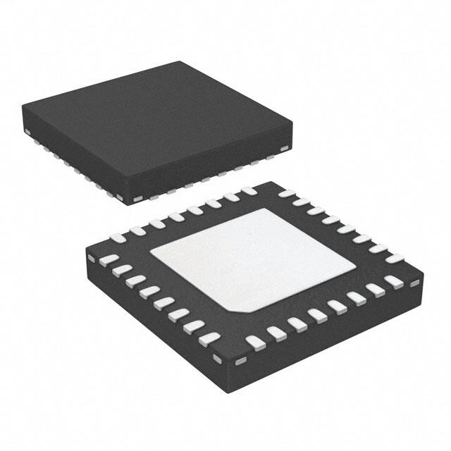
The Le75183 device is packaged in a 20-pin, plastic SOIC (GULL) (Le75183ASC/BSC/CSC/DSC), a 32-pin QFN (Le75183AQC/
BQC/CQC/DQC), and a 28-pin, plastic SOIC (GULL) (Le75183AESC/BESC/CESC/CZESC/DESC). The 28-pin package is
available to support existing designs. For new designs, it may be advantageous to use the other two packages for smaller in size.
3
Zarlink Semiconductor Inc.
�Le75183
Data Sheet
BLOCK DIAGRAMS
Figure 1.
Le75183A/C
Le75183A/C
VBAT
FGND
SCR
& Trip
Circuit
SW1
SW2
TTESTin
RBAT
TBAT
TLINE
SW3
SW4
SW5
SW6
TRINGING
RLINE
RRINGING
SW7
TTESTout
RTESTin
SW8
RTESTout
SW10
SW9
LATCH
VDD
Control
Logic
TSD
INTESTin
INRING
INTESTout
DGND
Figure 2.
Le75183B/D
Le75183B/D
VBAT
FGND
TTESTin
SW1
SW2
RBAT
TBAT
TLINE
SW3
SW4
SW5
SW6
RLINE
RRINGING
TRINGING
SW7
TTESTout
RTESTin
SW8
SW9
SW10
RTESTout
LATCH
VDD
Control
Logic
TSD
INTESTin
INRING
INTESTout
DGND
4
Zarlink Semiconductor Inc.
�Le75183
Data Sheet
NC
VBAT
NC
RTESTin
31
30
29
28
27
26
NC
NC
32
1
FGND
Top View
NC
TTESTin
CONNECTION DIAGRAMS
25
24
RBAT
23
NC
3
22
RLINE
4
21
NC
TBAT
2
NC
TLINE
32-pin QFN
NC
5
20
TRINGING
6
19
NC
NC
7
18
RTESTout
TTESTout
8
10
11
12
13
14
15
NC
TSD
DGND
INTESTout
INRING
INTESTin
28
VBAT
RTESTin
NC 2
27
NC
18
RBAT
NC 3
26
NC
17
RLINE
NC 4
25
NC
16
RRINGING
TTESTin 5
24
RTESTin
15
RTESTout
TBAT 6
23
RBAT
14
LATCH
TLINE 7
22
RLINE
TRINGING 8
21
NC
NC 9
20
RRINGING
TTESTout 10
19
RTESTout
NC 11
18
LATCH
VDD 12
17
INTESTin
TSD 13
16
INRING
DGND 14
15
INTESTout
1
20
VBAT
TTESTin
2
19
TBAT
3
TLINE
4
TRINGING
5
TTESTout
6
NC
7
NC
FGND 1
FGND
20-Pin SOIC
17
16
LATCH
9
VDD
EXPOSED PAD
RRINGING
VDD
8
13
INTESTin
TSD
9
12
INRING
DGND
10
11
INTESTout
28-Pin SOIC
5
Zarlink Semiconductor Inc.
�Le75183
Data Sheet
Pin Descriptions .
Pin Name
Type
DGND
Ground
Digital ground.
Description
FGND
Ground
Fault ground.
INRING
Input
Logic level switch input control. Internally 75 kΩ typical pull up.
INTESTIN
Input
Logic level switch input control. Internally 75 kΩ typical pull down.
INTESTOUT
Input
Logic level switch input control. Internally 75 kΩ typical pull up.
LATCH
Input
NC
—
Data input control, active-high, transparent low. Internally 75 kΩ typical pull down.
No connection.
RBAT
Input/Output
RLINE
Input/Output
Connect to RING on SLIC side.
Connect to RING on line side.
RRINGING
Input/Output
Connect to ringing generator.
RTESTin
Input/Output
Test (in) access on RING.
RTESTout
Input/Output
Test (out) access on RING.
TBAT
Input/Output
Connect to TIP on SLIC side.
TLINE
Input/Output
Connect to TIP on line side.
TRINGING
Input/Output
Connect to return ground for ringing generator.
TTESTin
Input/Output
Test (in) access on TIP.
TTESTout
Input/Output
Test (out) access on TIP.
TSD
Input/Output
Temperature shutdown pin. Can be used as a logic level input or an output. See Tables 12
and 13, Truth Tables, and the Switching Behavior section of this data sheet for input pin
description. As an output flag, will read HIGH when the device is in its operational mode
and LOW in the thermal shutdown mode. To disable the thermal shutdown mechanism, tie
this pin to HIGH (not recommended)
VBAT
Battery
Battery voltage. Used as a reference for protection circuit.
VDD
Power
5 V supply.
EPAD
—
Exposed pad in QFN package. No internal electrical connection. Not recommended to
make any external electrical connection (such as VBAT or ground) to the EPAD.
D: Internally 75 kΩ typical pull down.
U: Internally 75 kΩ typical pull up.
6
Zarlink Semiconductor Inc.
�Le75183
Data Sheet
ABSOLUTE MAXIMUM RATINGS
Stresses above those listed under Absolute Maximum Ratings can cause permanent device failure. Functionality at or above
these limits is not implied. Exposure to absolute maximum ratings for extended periods may affect device reliability.
Parameter
Min
Max
Unit
Operating Temperature Range
Storage Temperature Range
Relative Humidity Range
Pin Soldering Temperature (t=10s max)
5 V Power Supply
Battery Supply
Logic Input Voltage
Input-to-output Isolation
Pole-to-pole Isolation (All except SW6, SW8)
Pole-to-pole Isolation (Ringing Access Switch, SW8)
Pole-to-pole Isolation (Ringing Test Swtich, SW6)
ESD Immunity (Human Body Model)
–40
110
°C
–40
150
°C
5
95
%
—
260
°C
-0.3
7
V
—
–85
V
V
-0.3
VDD+0.3
—
330
V
—
330
V
—
480
V
—
260
V
JESD22 Class 1C compliant
Note:
For LCAS in the QFN package, it is desirable that the exposed pad be soldered to an equally sized exposed copper surface (with no
further electrical connection such as VBAT or ground) for mechanical stability.
OPERATING RANGES
Package Assembly
Green package devices are assembled with enhanced, environmental compatible lead-free, halogen-free, and antimony-free
materials. The leads possess a matte-tin plating which is compatible with conventional board assembly processes or newer leadfree board assembly processes. The peak soldering temperature should not exceed 245°C during printed circuit board assembly.
Refer to IPC/JEDEC J-Std-020B Table 5-2 for the recommended solder reflow temperature profile.
Environmental Ranges
Legerity guarantees the performance of this device over commercial (0 to 70º C) and industrial (-40 to 85ºC) temperature ranges
by conducting electrical characterization over each range and by conducting a production test with single insertion coupled to
periodic sampling. These characterization and test procedures comply with section 4.6.2 of Bellcore GR-357-CORE Component
Reliability Assurance Requirements for Telecommunications Equipment.
−40° to 85°C
Ambient Temperature
Electrical Ranges
Min
Typ
Max
Unit
VDD
Supply
4.5
5
5.5
V
VBAT*
–19
—
–72
V
*VBAT is used only as a reference for internal protection circuitry. If VBAT rises above typically –10 V, the device will enter an all OFF state and
remain in this state until the battery voltage drops below typically –15 V.
*Applied voltage is 100 Vp-p square wave at 100 Hz.
Handling Precautions
Although protection circuitry has been designed into this device, proper precautions should be taken to avoid exposure to electrostatic discharge (ESD) during handling and mounting. Legerity employs a human-body model (HBM) and a charged-device
model (CDM) for ESD-susceptibility testing and protection design evaluation. ESD voltage thresholds are dependent on the
circuit parameters used to define the model. No industry-wide standard has been adopted for CDM. However, a standard HBM
(resistance = 1500Ω , capacitance = 100 pF) is widely used and therefore can be used for comparison purposes. The HBM ESD
threshold presented here was obtained by using these circuit parameters.
7
Zarlink Semiconductor Inc.
�Le75183
Data Sheet
ELECTRICAL CHARACTERISTICS
Summary of Assumptions
Unless otherwise noted, the test conditions are defined by the Le75183 device application circuit shown in Figure 8, on page 19
with:
VBAT = −48 V, VDD = 5.0 V.
Supply Currents and Power Dissipation
IBAT µA
IDD mA
Operational State
LCAS Device Power mW
Condition
Min.
Typ
Max
Min.
Typ
Max
Min.
Typ
Max
All OFF
VDD=5V, VBAT=-48V
—
0.760
1.1
—
4
10
—
3.8
6
Power Ringing or
Access
VDD=5V, VBAT=-48V
—
0.850
2.1
—
4
10
—
4.4
11
Idle/Talk
VDD=5V, VBAT=-48V
—
0.860
1.3
—
4
10
—
4.5
7
SPECIFICATIONS
Device Specifications
Table 1. Test-In Switches, 1 and 2
Parameter
Test Condition
Measure
Min
Typ
Max
ISWITCH
—
—
1
ISWITCH
—
—
1
ISWITCH
—
—
1
Unit
OFF-state Leakage Current:
+25°C
+85°C
–40°C
Vswitch (differential) = –320 V to Gnd
Vswitch (differential) = –60 V to +260 V
Vswitch (differential) = –330 V to Gnd
Vswitch (differential) = –60 V to +270 V
Vswitch (differential) = –310 V to Gnd
Vswitch (differential) = –60 V to +250 V
µA
ON-resistance (SW1, SW2):
+25 °C
ISWITCH (on) = ±5 mA, ±10 mA
∆ VON
—
49
—
+85 °C
ISWITCH (on) = ±5 mA, ±10 mA
∆ VON
—
—
77
–40 °C
ISWITCH (on) = ±5 mA, ±10 mA
∆ VON
—
37
—
+25 °C
Vswitch (both poles) = ±320 V, Logic inputs = Gnd
Iswitch
—
—
1
+85 °C
Vswitch (both poles) = ±330 V, Logic inputs = Gnd
Iswitch
—
—
1
–40 °C
Vswitch (both poles) = ±310 V, Logic inputs = Gnd
Iswitch
—
—
1
—
—
200
—
Ω
Isolation:
dV/dt Sensitivity*
—
*Applied voltage is 100 Vp-p square wave at 100 Hz. Not tested in production.
8
Zarlink Semiconductor Inc.
µA
V/µs
�Le75183
Data Sheet
Table 2. Break Switches, 3 and 4
Parameter
Test Condition
Measure
Min
Typ
Max
ISWITCH
—
—
1
ISWITCH
—
—
1
ISWITCH
—
—
1
21.5
—
Unit
OFF-state Leakage Current:
+25°C
+85°C
–40°C
Vswitch (differential) = –320 V to Gnd
Vswitch (differential) = –60 V to +260 V
Vswitch (differential) = –330 V to Gnd
Vswitch (differential) = –60 V to +270 V
Vswitch (differential) = –310 V to Gnd
Vswitch (differential) = –60 V to +250 V
µA
ON-resistance (SW3, SW4):
+25 °C
TLINE = ±10 mA, ±40 mA, TBAT = –2 V
∆ VON
—
+85 °C
TLINE = ±10 mA, ±40 mA, TBAT = –2 V
∆ VON
—
—
31
–40 °C
TLINE = ±10 mA, ±40 mA, TBAT = –2 V
∆ VON
—
16
—
Per ON-resistance test condition of SW3, SW4
Magnitude
RON_SW3 – RON_SW4
—
0.2
1.0
Ω
Per ON-resistance test condition of SW3, SW4
Magnitude
RON_SW3 – RON_SW4
—
0.2
0.55
Ω
Iswitch = ILIMIT @ 50 Hz/60 Hz
VON
—
—
220
V
ON-resistance Match
All except Le75183CZESC
ON-resistance Match
Le75183CZESC
ON-state Voltage*
(Figure 2, Switch 3)
ON-state Voltage*
(Figure 3, Switch 4)
Maximum Differential Voltage (Vmax)
VON
—
—
320
Foldback Voltage Breakpoint 1 (V1)
VON
100
—
—
Foldback Voltage Breakpoint 2 (V2)
VON
V1+0.5
—
—
Vswitch (on) = ±10 V
Iswitch
80
—
—
Ω
V
DC Current Limit
(Figure 2, Switch 3):
+85 °C
Vswitch (on) = ±10 V
Iswitch
—
—
250
DC Current Limit
ILIMIT1
Iswitch
80
—
250
(Figure 3, Switch 4):
ILIMIT2
Iswitch
2
—
—
Dynamic Current Limit
(t =