TM
Le87213A
Worldwide xDSL Dual Channel Line Driver
BD870 Series
APPLICATIONS
DESCRIPTION
Asymmetrical Digital Subscriber Loop (ADSL, ADSL+,
The Le87213A device, from the Zarlink Battery Direct™
family BD870 series devices, integrates two fully differential
line drivers, optimized feed back components, on-chip surge
protection diodes and bias control stages into a small
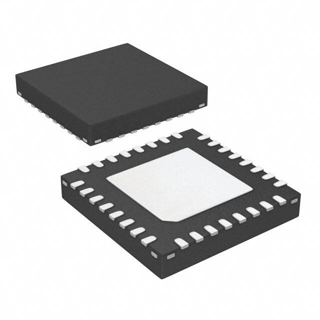
8 x 8 mm2 QFN package. It contains all the active components
needed to implement ADSL2+ downstream transmitters for two
lines. The Le87213A device is built on Zarlink’s high-voltage
process that allows for direct operation from a standard
telecom, negative battery supply (and a 3.3-V supply). In
contrast, typical line cards today supply the power to the line
drivers locally, via DC-to-DC converter modules. The
elimination of these additional modules translates into cost and
power savings at the system level. Operation from a
centralized source of power makes the Le87213A device a
unique, less costly, more efficient solution for xDSL line driver
applications. The Le87213A device is one of the most costeffective and easy-to-use parts for today’s xDSL applications.
ADSL2, ADSL2+) Line Drivers
G.lite Line Drivers
HDSL, HDSL2, HDSL4, SHDSL Line Drivers
DSLAM, CO, DLC, BLC, MDU/MTU Line Drivers
FEATURES
Two-channel differential line drivers
Low power
— 720 mW per channel, typical (ADSL+ Mode)
(showtime, >5 kft 26 AWG cable, not including load)
— 670 mW per channel, typical (ADSL Mode)
(showtime, >5 kft 26 AWG cable, not including load)
Operates directly from a typical telecom power supply
without a DC-to-DC converter and a 3.3 V supply
Integrated lightning and surge protection
50 VP differential signal at the driver outputs
IOUT max 95 mA into 100-Ω load
MTPR of 70 dB, typical
Minimum external component count ~ 10 discretes per
channel
Can output 20.8 dBm power into 100-Ω load with step
down transformer
Thermal shutdown
Small footprint
BLOCK DIAGRAM
VCC
VBAT
AGND
BGND
–
AY1
DDWNP1
+
— 32-pin (8 x 8 mm) QFN
+
–
RELATED LITERATURE
+
080791 Quad Flat No-Lead (QFN) Package
–
ORDERING INFORMATION
AY2
+
Packing2
+
–
32-pin QFN, 8 x 8 mm
Tray
(Green Package)1
1.
The green package meets RoHS Directive 2002/95/EC of the
European Council to minimize the environmental impact of
electrical equipment.
2.
For delivery using a tape and reel packing system, add a "T" suffix
to the OPN (Ordering Part Number) when placing an order.
VBIAS
+
BY2
DDWNN2
–
CONTROL
LOGIC1
CONTROL
LOGIC2
DISCON2
32-pin QFN, 8 x 8 mm
PDOWN1
Le87213AFQC
–
DDWNP2
DISCON1
Le87213AQC
Package
BY1
DDWNN1
Application Note
Device
VBIAS
PDOWN2
Document ID# 081247 Date:
Rev:
B
Version:
Public Document
Distribution:
Sep 20, 2007
2
�Le87213A
Data Sheet
TABLE OF CONTENTS
Applications . . . . . . . . . . . . . . . . . . . . . . . . . . . . . . . . . . . . . . . . . . . . . . . . . . . . . . . . . . . . . . . . . . . . . . .1
Features . . . . . . . . . . . . . . . . . . . . . . . . . . . . . . . . . . . . . . . . . . . . . . . . . . . . . . . . . . . . . . . . . . . . . . . . . .1
Related literature . . . . . . . . . . . . . . . . . . . . . . . . . . . . . . . . . . . . . . . . . . . . . . . . . . . . . . . . . . . . . . . . . . .1
Ordering Information . . . . . . . . . . . . . . . . . . . . . . . . . . . . . . . . . . . . . . . . . . . . . . . . . . . . . . . . . . . . . . .1
Description. . . . . . . . . . . . . . . . . . . . . . . . . . . . . . . . . . . . . . . . . . . . . . . . . . . . . . . . . . . . . . . . . . . . . . . .1
Block Diagram . . . . . . . . . . . . . . . . . . . . . . . . . . . . . . . . . . . . . . . . . . . . . . . . . . . . . . . . . . . . . . . . . . . .1
Product Description . . . . . . . . . . . . . . . . . . . . . . . . . . . . . . . . . . . . . . . . . . . . . . . . . . . . . . . . . . . . . . . .3
Lightning and Power Surges . . . . . . . . . . . . . . . . . . . . . . . . . . . . . . . . . . . . . . . . . . . . . . . . . . . . . .3
Block Description . . . . . . . . . . . . . . . . . . . . . . . . . . . . . . . . . . . . . . . . . . . . . . . . . . . . . . . . . . . . . . .3
Downstream Path . . . . . . . . . . . . . . . . . . . . . . . . . . . . . . . . . . . . . . . . . . . . . . . . . . . . . . . . . . . . . .3
Control Logic . . . . . . . . . . . . . . . . . . . . . . . . . . . . . . . . . . . . . . . . . . . . . . . . . . . . . . . . . . . . . . . . . .3
Device Operating Modes. . . . . . . . . . . . . . . . . . . . . . . . . . . . . . . . . . . . . . . . . . . . . . . . . . . . . . . . . . . . .3
Active Mode . . . . . . . . . . . . . . . . . . . . . . . . . . . . . . . . . . . . . . . . . . . . . . . . . . . . . . . . . . . . . . . . . . .3
PDown Mode . . . . . . . . . . . . . . . . . . . . . . . . . . . . . . . . . . . . . . . . . . . . . . . . . . . . . . . . . . . . . . . . . .3
Disconnect Mode . . . . . . . . . . . . . . . . . . . . . . . . . . . . . . . . . . . . . . . . . . . . . . . . . . . . . . . . . . . . . . .3
Operating Mode Control Decoding . . . . . . . . . . . . . . . . . . . . . . . . . . . . . . . . . . . . . . . . . . . . . . . . .3
Connection Diagram . . . . . . . . . . . . . . . . . . . . . . . . . . . . . . . . . . . . . . . . . . . . . . . . . . . . . . . . . . . . . . . .4
Pin Descriptions . . . . . . . . . . . . . . . . . . . . . . . . . . . . . . . . . . . . . . . . . . . . . . . . . . . . . . . . . . . . . . . . . . .4
Absolute Maximum Ratings . . . . . . . . . . . . . . . . . . . . . . . . . . . . . . . . . . . . . . . . . . . . . . . . . . . . . . . . . .5
Thermal Resistance . . . . . . . . . . . . . . . . . . . . . . . . . . . . . . . . . . . . . . . . . . . . . . . . . . . . . . . . . . . . .5
Package Assembly . . . . . . . . . . . . . . . . . . . . . . . . . . . . . . . . . . . . . . . . . . . . . . . . . . . . . . . . . . . . .5
Operating Ranges . . . . . . . . . . . . . . . . . . . . . . . . . . . . . . . . . . . . . . . . . . . . . . . . . . . . . . . . . . . . . . . . . .5
Electrical Characteristics . . . . . . . . . . . . . . . . . . . . . . . . . . . . . . . . . . . . . . . . . . . . . . . . . . . . . . . . . . . .6
Supply Currents and Power Consumption. . . . . . . . . . . . . . . . . . . . . . . . . . . . . . . . . . . . . . . . . . . .6
Test Circuit. . . . . . . . . . . . . . . . . . . . . . . . . . . . . . . . . . . . . . . . . . . . . . . . . . . . . . . . . . . . . . . . . . . . . . . .6
Specifications . . . . . . . . . . . . . . . . . . . . . . . . . . . . . . . . . . . . . . . . . . . . . . . . . . . . . . . . . . . . . . . . . . . . .7
Device Specifications. . . . . . . . . . . . . . . . . . . . . . . . . . . . . . . . . . . . . . . . . . . . . . . . . . . . . . . . . . . .7
Application Circuit. . . . . . . . . . . . . . . . . . . . . . . . . . . . . . . . . . . . . . . . . . . . . . . . . . . . . . . . . . . . . . . . . .8
PCB Layout . . . . . . . . . . . . . . . . . . . . . . . . . . . . . . . . . . . . . . . . . . . . . . . . . . . . . . . . . . . . . . . . . . .8
Physical Dimensions. . . . . . . . . . . . . . . . . . . . . . . . . . . . . . . . . . . . . . . . . . . . . . . . . . . . . . . . . . . . . . . .9
32-Pin QFN . . . . . . . . . . . . . . . . . . . . . . . . . . . . . . . . . . . . . . . . . . . . . . . . . . . . . . . . . . . . . . . . . . .9
Device Operational Notes . . . . . . . . . . . . . . . . . . . . . . . . . . . . . . . . . . . . . . . . . . . . . . . . . . . . . . . . . . .10
Power Supplies . . . . . . . . . . . . . . . . . . . . . . . . . . . . . . . . . . . . . . . . . . . . . . . . . . . . . . . . . . . . . . .10
Line Transformer . . . . . . . . . . . . . . . . . . . . . . . . . . . . . . . . . . . . . . . . . . . . . . . . . . . . . . . . . . . . . .10
Transformer Turns Ratio . . . . . . . . . . . . . . . . . . . . . . . . . . . . . . . . . . . . . . . . . . . . . . . . . . . . . . . .11
Downstream Filtering . . . . . . . . . . . . . . . . . . . . . . . . . . . . . . . . . . . . . . . . . . . . . . . . . . . . . . . . . . .11
Receiver and Hybrid Circuit . . . . . . . . . . . . . . . . . . . . . . . . . . . . . . . . . . . . . . . . . . . . . . . . . . . . . . . . .11
Components Selection . . . . . . . . . . . . . . . . . . . . . . . . . . . . . . . . . . . . . . . . . . . . . . . . . . . . . . . . . . . . .12
Revision History . . . . . . . . . . . . . . . . . . . . . . . . . . . . . . . . . . . . . . . . . . . . . . . . . . . . . . . . . . . . . . . . . .13
Revision A1 to B1 . . . . . . . . . . . . . . . . . . . . . . . . . . . . . . . . . . . . . . . . . . . . . . . . . . . . . . . . . . . . .13
Revision B1 to B2 . . . . . . . . . . . . . . . . . . . . . . . . . . . . . . . . . . . . . . . . . . . . . . . . . . . . . . . . . . . . .13
2
Zarlink Semiconductor Inc.
�Le87213A
Data Sheet
PRODUCT DESCRIPTION
The Le87213A device is a low-power, dual xDSL differential line driver. It is part of Zarlink’s family of integrated line drivers
capable of operating from a standard negative battery supply. Its integration of feedback components and on-chip surge
protection diodes makes it one of the most integrated line drivers on the market today.
The Le87213A device was designed on a high voltage, high bandwidth bipolar process in which fast slew rate and low distortion
amplifiers were implemented. It requires one line transformer per line for isolation and for compliance with IEC60950-1, 2001 and
UL60950 standards. The line driver amplifiers in the Le87213A device were designed with an optimized bandwidth for xDSL
applications as well as for fast slew rates of 300 V/µs.
Lightning and Power Surges
The Le87213A device has built-in lightning and power surge protection. When used with the components listed in the PCB Layout,
on page 8, it needs no other external protector to meet the requirements for ADSL line Cards.
Block Description
Refer to the datapath provider for the application circuit.
Downstream Path
The downstream signal is applied at the DDWNP/DDWNN pins, and is amplified by a fixed voltage gain (KDWN) before being
applied to the AY and BY pins. The amplifiers driving the AY and BY pins are DC biased to approximately one-half of the VBAT
pin voltage. The typical differential output voltage swing between AY and BY pins is |VBAT| - 4 V. This allows the use of a stepdown transformer for the line interface.
Control Logic
This block controls the bias currents of the input stage and the bias current of the output amplifiers as described in the Device
Operating Modes section below.
DEVICE OPERATING MODES
The two lines of the Le87213A are completely independent and can be programmed to be in different operating modes. The logic
signal level of pins DISCON1 an Pdown1 controls the operating mode of line 1, the logic signal level of pins DISCON2 and
Pdown2 controls the operating mode of line 2.
Active Mode
In this mode, all stages are biased and operational.
PDown Mode
In this mode, the line driver amplifier’s power consumption is reduced. The Bias current in the output stage drops to almost half
full power stage. The part is ADSL compliant in this stage.
Disconnect Mode
In this mode, the bias is turned OFF to all stages to save power. The device is not operational.
Operating Mode Control Decoding
DISCON1
Pdown1
Line 1 Operating Mode
0
0
Active
0
1
Pdown
1
x
Disabled
DISCON2
Pdown2
Line 2 Operating Mode
0
0
Active
0
1
Pdown
1
x
Disabled
3
Zarlink Semiconductor Inc.
�Le87213A
Data Sheet
N/C
BY2
N/C
N/C
N/C
AY1
32
1
BGND
N/C
VBAT
Top View
BY1
CONNECTION DIAGRAM
31
30
29
28
27
26
25
24
AY2
2
23
N/C
N/C
3
22
N/C
N/C
4
21
N/C
N/C
5
20
N/C
DDWNN 1
6
19
N/C
DDWNP 1
7
18
DDWNN 2
N/C
8
DDWNP 2
Le87213A
Le87220QC
32-pin QFN
9
10
11
12
13
14
15
17
16
N/C
PDOWN 1
DISCON1
N/C
AGND
VCC
PDOWN 2
DISCON2
EXPOSED PAD
Notes:
1.
Pin 1 is marked for orientation.
2.
The Le87213A device incorporates an exposed die pad on the underside of its package. The pad acts as a heat sink and must be connected
to a copper plane through thermal vias, for proper heat dissipation (See PCB Layout, on page 8.).
PIN DESCRIPTIONS
Pin
Pdown1, Pdown2
DDWNP1, DDWNN1,
DDWNP2, DDWNN2
Pin Name
Type
Control Bits
Description
Input
Active/Pdown mode control bit.
Differential Downstream
Input
The differential downstream signal from the data AFE is AC
coupled to these pins.
Input
Disables the line completely by pulling it to VCC.
DISCON1, DISCON2
Disconnect
AY1, BY1
AY2, BY2
A/B Line Driver
VBAT
Negative Battery
Power
Negative power supply.
VCC
Power Supply
Power
+3.3 V analog power supply.
AGND
Analog Ground
Ground
Low voltage ground return.
BGND
Battery Ground
Ground
Battery ground return.
N/C
No Connect
EXPOSED PAD
Output
Differential downstream line driver outputs.
Not connected.
Isolated
Exposed pad on underside of device must be connected to
a heat spreading area. The AGND plane is recommended.
4
Zarlink Semiconductor Inc.
�Le87213A
Data Sheet
ABSOLUTE MAXIMUM RATINGS
Stresses above the values listed under Absolute Maximum Ratings can cause permanent device failure. Functionality at or above
these limits is not implied. Exposure to absolute maximum ratings for extended periods can affect device reliability.
Storage Temperature
−55 ≤ TA ≤ +150°C
Ambient temperature, under bias
VCC with respect to AGND
−0.4 V to +6 V
−40 ≤ TA ≤ +85°C
VBAT with respect to BGND
BGND with respect to AGND (1 ms)
Maximum Current into AY, BY
Continuous
100 µs (F = 0.1 Hz)
1 µs (F = 0.1 Hz)
250 ns (F = 0.1 Hz)
Peak current output, AY or BY pins
Pdown, DISCON pins with respect to AGND
Maximum Power Dissipation, TA = 85°C
(See Notes 1 and 2)
ESD Immunity (Human Body Model)
ESD Immunity (Charge Device Model)
+0.4 V to -75 V
−5.5 V to +0.2 V
±200 mA
±1 A
±2.5 A
±5.5 A
±200 mA
–0.4 V to (VCC + 0.4 V)
2W
JESD22 Class 1C compliant
Class C6 1500 - 2000 V
Note:
1.
Thermal limiting circuitry on chip will shut down the circuit at a junction temperature of about 165°C. Continuous operation above 145°C
junction temperature may degrade device reliability.
2.
The thermal performance of a thermally enhanced package is assured through optimized printed circuit board layout. Specified performance
requires that the exposed thermal pad be soldered to an equally sized exposed copper surface, which, in turn, conducts heat through
multiple vias to a large internal copper plane (See PCB Layout, on page 8.).
Thermal Resistance
The junction to air thermal resistance of the Le87213A device in a 32-pin QFN package is 30°C/W (measured with infinite external
heat sinking). Please refer to Zarlink’s QFN Package application note, available from http://www.zarlink.com , for layout and heat
sinking guidelines.
Package Assembly
The standard (non-green) package devices are assembled with industry-standard mold compounds, and the leads possess a tin/
lead (Sn/Pb) plating. These packages are compatible with conventional SnPb eutectic solder board assembly processes. The
peak soldering temperature should not exceed 225°C during printed circuit board assembly.
The green package devices are assembled with enhanced, environmental compatible lead-free, halogen-free, and antimony-free
materials. The leads possess a matte-tin plating which is compatible with conventional board assembly processes or newer leadfree board assembly processes. The peak soldering temperature should not exceed 245°C during printed circuit board assembly.
Refer to IPC/JEDEC J-Std-020B Table 5-2 for the recommended solder reflow temperature profile.
OPERATING RANGES
Zarlink guarantees the performance of this device over commercial (0°C to 70°C) and industrial (−40°C to 85°C) temperature
ranges by conducting electrical characterization over each range and by conducting a production test with single insertion coupled
with periodic sampling. These characterization and test procedures comply with section 4.6.2 of Bellcore GR-357-CORE
Component Reliability Assurance Requirements for Telecommunications Equipment.
Ambient temperature
-40°C to +85°C
VCC
+3.3 V ± 5%
VBAT
-42 V to -72 V
BGND with respect to AGND
-2 to +0.1VDC
The Le87213A is designed to operate with a standard telecom battery. The normal operating voltage of such batteries is -52 V,
and the Le87213A is designed to give optimal performance in terms of power dissipation if used with the provided applications
circuit. However, because the Le87213A is designed on Zarlink’s proprietary high voltage, high bandwidth process, the part will
continue to remain in operation without any degradation in data performance should the battery drop to as low as -42 V, or charge
to as high as -72 V. Should there be a need to operate the part continuously at such voltages, a different applications circuit should
be considered to achieve best power performance. Lower voltage operation can be achieved by adding a buck-boost regulator.
The Le87213A is designed to operate with the T1.315 specified telecom battery, without any need for changes in the reference
design.
5
Zarlink Semiconductor Inc.
�Le87213A
Data Sheet
ELECTRICAL CHARACTERISTICS
VBAT = -52 V, VCC = +3.3 V, TA = 25°C unless otherwise specified.
Supply Currents and Power Consumption
Values listed in the table below are per line, and include the load power.
VBAT (mA)
Operational
State
Active
Condition
TA
Min
Typ
Device Power
(mW)
VCC (mA)
Max
Min
Typ
Max
Min
Typ
Training at 5 kft 26 AWG cable
25°C
16
5.3
850
Showtime at 5 kft 26 AWG cable,
19.85 dBm
25°C
15.5
5.3
824
25°C
15.5
5.3
824
Full
range
15.5
5.6
826
25°C
14.5
5.3
772
Full
range
14.5
5.3
772
Full
range
1
5.3
65
19.85 dBm signal into 100 Ω load
with 2.45:1 transformer
Pdown
Disconnect
Max
1.
Note:
1.
In the Active state, 96.6 mW is dissipated in the loop and 7.5 mW is dissipated in the transformer plus the series drive resistors.
For device power dissipation, subtract these values from the numbers listed in the table above.
TEST CIRCUIT
Only one of two channels is shown.
U1
VCC
+ 3.3 V
VBAT
Le87213A
Le87220
+
–
C8
–
C9
AGND
+
52 V
BGND
–
+
R10
R2
T1
AY1
RSEC1
VTX
+
–
R1 VDWN
VAY,BY
VBIAS
VLOOP
C5
R11
C2
C6
DDWNN1
+
R3
RSEC2
BY1
–
PDOWN1
DISCON1
CONTROL
LOGIC1
Control Logic Circuit
Note:
1.
TIP(A)1
RPRI1
DDWNP1
C1
Component values are the same as those listed in the PCB Layout, on page 8 unless otherwise noted.
6
Zarlink Semiconductor Inc.
RPRI2
RING(B)1
Note
ZLOOP
�Le87213A
Data Sheet
SPECIFICATIONS
Device Specifications
Typical Conditions: VBAT = −52 V, VCC = 3.3 V, Transformer Turns Ratio = 2.45:1
Min/Max Parameters: T = −40 to +85°C; Typ, TA = 25°C, Pdown=0 (Full Power)
Note:
Parameters in the following "Device Specifications" tables are guaranteed by characterization. Refer to Test Circuit, on page 6.
Table 1. Pdown = 0 (Full Power)
Specification
Condition
Min
Typ
Max
Unit
0.6
1.0
µV
----------Hz
28k
40k
52k
kΩ
V BAT
---------------- – 0.25
2
V BAT
---------------- + 0.75
2
V BAT
---------------- + 1.75
2
V
Note
AC Characteristics
VnDWN
Output Differential Noise Voltage,
at (AY, BY)
VTX=0 V, 25 kHz to 2208 kHz
RDDWN
Differential Input Impedance DDWNP to
DDWNN
VAYDC, VBYDC
AY, BY DC bias voltage
VCC to AY, BY
PSRRVCC
All operating Modes
VBAT to AY, BY
PSRRVBAT
All operating Modes
BGND to AY, BY
PSRRBDND
Crosstalk between lines
All operating Modes
Xtalk
20 kHz
400 kHz
800 kHz
–38
2 MHz
–20
20 kHz
400 kHz
800 kHz
–50
2 MHz
–32
20 kHz
400 kHz
800 kHz
–50
2 MHz
–50
–26
-24
–44
dB
-37
–50
-50
fc=100 kHz, Vout=2Vpp
70
80
fc=2208 kHz, Vout=2Vpp
50
60
dB
VIN, DWN
Input Amplitude, AC coupled
1.0
V
Iout, max
Iout max into 100 ohm load
95
mA
1., 2.
Logic Inputs (Pdown1, Pdown2, DISCON1 and DISCON2)
VIH
Logic 1, High level Input voltage
2
VCC
VIL
Logic 0, Low level Input voltage
AGND
0.8
IIH
Pdown = VCC
100
IIL
Pdown = AGND
-100
IIH
DISCON = VCC
100
IIL
DISCON = AGND
-100
V
µA
Device Performance:
SR
Slew Rate at VAY–BY
300
V/µs
HD2
fc=1MHz, RL=100Ohms, Vout=2Vp-p
-70
dBc
HD3
fc=1MHz, RL=100Ohms, Vout=2Vp-p
-70
dBc
MTPR
Downstream multitone power ratio ITU,
G.992.1 MTPR test peak to rms ratio = 5.8
70
dB
KDWN
KDWN = VAY,BY/VDWN
25 kHz to 2208 kHz
46
KDWN vs. frequency
-3 dB
5
250
7
Zarlink Semiconductor Inc.
48
50
V/V
MHz
3.
�Le87213A
Data Sheet
Table 2. Pdown = 1 (Power Down)
Specification
Condition
Min
Typ
Max
Unit
0.6
1.0
µV
----------Hz
40k
52k
kΩ
V
BAT
---------------- + 1.75
2
V
Note
AC Characteristics
VnDWN
Output Differential Noise Voltage,
at (AY, BY)
VTX=0 V, 25 kHz to 1104 kHz
RDDWN
Differential Input Impedance DDWNP to
DDWNN
VAYDC, VBYDC
AY, BY DC bias voltage
Crosstalk
between lines
Xtalk
28k
V
V
BAT
BAT
---------------- – 0.25 ---------------- + 0.75
2
2
fc=100 kHz, Vout=2Vpp
70
80
fc=1104 kHz, Vout=2Vpp
50
60
dB
VIN, DWN
Input Amplitude, AC coupled
1.0
V
Iout, max
Iout max into 100 ohm load
80
mA
1., 2.
Device Performance:
SR
Slew Rate at VAY–BY
250
V/µs
HD2
fc=1MHz, RL=100Ohms, Vout=2Vp-p
-67.5
dBc
HD3
fc=1MHz, RL=100Ohms, Vout=2Vp-p
-67.5
dBc
MTPR
Downstream multitone power ratio ITU,
G.992.1 MTPR test peak to rms ratio = 5.8
67.5
dB
KDWN
KDWN = VAY,BY/VDWN
25 kHz to 1104 kHz
46
KDWN
vs. frequency
-3 dB
4
200
48
50
3.
V/V
MHz
Notes:
1.
Crosstalk is measured with one line transmitting signal, the other line is enabled but VTX is set to 0 V.
2.
V ( AY, BY )1
Crosstalk: Xtalk ( dB ) = 20 log ---------------------------------
V ( AY, BY )2
3.
Measured with a 2.45:1 transformer and a 100-Ω load.
APPLICATION CIRCUIT
Refer to the datapath reference design.
PCB Layout
The Le87213A device contains high gain and high bandwidth amplifiers. The amplifier inputs of each line are connected to the
DDWNP/DDWNN pins, the output are connected to the AY and BY pins. To prevent coupling of the high level output signals into
the low level DDWNP/DDWNN pins, PCB tracks and components connected to AY, BY, and going to the TIP (A) and RING (B)
terminals must be well separated from tracks connected to DDWNP/DDWNN pins. The components C1, C2, R1, R10, and R11
(and the corresponding components of line 2) should be as close as practical to DDWNP/DDWNN pins. The Le87213A device
provides an analog ground pin (AGND) as a return for low level currents and a battery ground pin (BGND) as a return for high
level currents.
The differential drivers of the Le87213A device do not produce any load current into the AGND leads, but the amplifier currents
are still circulating in the VBAT and BGND pins. A bypass capacitor between VBAT and BGND is required to be close to the
device. AGND and BGND tracks should only be tied together at a single point, close to the power connector of the card.
The Le87213A device uses a thermally enhanced package equipped with an exposed pad on the bottom side. The printed circuit
board surface must have a copper pad covering the full surface of the thermal pad. The copper pad must be fitted with a minimum
of 16 thermal transfer vias on a 1 mm pitch with a via diameter of 0.3 to 0.33 mm, and be connected to a large internal copper
plane for proper heat dissipation. The AGND plane is recommended. The thermal transfer vias should be connected to the
thermal pad and to the AGND plane without thermal relieve tracks. The AGND plane should be the second layer from the top of
the PCB for the best power dissipation.
In multi-line applications, the Le87213A devices must be positioned in the layout to ensure a minimum distance of 1 inch (center
to center) between devices. Passive non-heat producing components can be placed between the Le87213A devices.
8
Zarlink Semiconductor Inc.
�Le87213A
Data Sheet
PHYSICAL DIMENSIONS
32-Pin QFN
Symbol
A
A2
b
D
D2
E
E2
e
L
N
A1
A3
aaa
bbb
ccc
Min
0.80
0.18
5.70
5.70
0.43
0.00
32 LEAD QFN
Nom
0.90
0.57 REF
0.23
8.00 BSC
5.80
8.00 BSC
5.80
0.80 BSC
0.53
32
0.02
0.20 REF
0.20
0.10
0.10
Max
1.00
0.28
5.90
5.90
0.63
NOTES:
1. Dimensioning and tolerancing conform to ASME Y14.5M-1994.
2. All dimensions are in millimeters.
is in degrees.
3. N is the total number of terminals.
4. The Terminal #1 identifier and terminal numbering convention
shall conform to JEP 95-1 and SSP-012. Details of the Terminal #1
identifier are optional, but must be located within the zone
indicated. The Terminal #1 identifier may be either a mold or
marked feature.
5. Coplanarity applies to the exposed pad as well as the terminals.
6. Reference Document: JEDEC MO-220.
7. Lead width deviates from the JEDEC MO-220 standard.
0.05
32-Pin QFN
Note:
Packages may have mold tooling markings on the surface. These markings have no impact on the form, fit or function of the device. Markings will vary with the mold tool used in manufacturing.
9
Zarlink Semiconductor Inc.
�Le87213A
Data Sheet
DEVICE OPERATIONAL NOTES
Power Supplies
The Le87213A device is implemented in a high-voltage process that allows direct powering from the –42 V to –72 V battery supply
without the need for DC to DC converters. This saves significant power that would otherwise be wasted in the DC to DC converter.
The noise on (referenced to AGND) the battery supply (VBAT pin) and on the +3.3 V supply (VCC pin) should be below the limits
as shown in Figure 1, in order not to affect the data performance.
Figure 1.
Allowed Noise on Power Supply Pins (Referenced to AGND)
140
120
noise uV/rtHz
100
80
VBAT
VCC
60
40
20
0
0
100
200
300
400
500
600
700
800
900
1000
1100
1200
frequency kHz
Line Transformer
A step-down transformer is used to interface the Le87213A device with the TIP (A) and RING (B) line terminals. The transformer
injects the data signal onto the loop and provides dielectric isolation and impedance matching between the loop and the line driver.
The turn ratio of the transformer can be optimized to match the loop signal level to the driver output swing (see Transformer Turns
Ratio, on page 11).
Transformer Specifics
Figure 2 represents a simplified transformer model in which the boxed block is an ideal transformer with an infinite bandwidth.
Figure 2.
Le87213A Transformer
TIP(A)
RPRI
RSEC
ZSEC
LLEAK
Secondary
Primary
LPRI
`
ZINTR
RING(B)
CPRI
N:1
10
Zarlink Semiconductor Inc.
�Le87213A
Data Sheet
Transformer Turns Ratio
The transformer turns ratio N is restricted by the maximum peak differential signal at AY/BY pins, which must stay within the
Le87213A device's dynamic range. The output voltage range is typically equal to |VBATmin| – 4 V.
The maximum peak voltage (across 100 Ω at TIP (A) and RING (B) leads of a FDM ADSL signal using 224 downstream carriers
for a combined rms power of 19.85 dBm and a peak-to-rms ratio of 5.8) is 36.05 VPP differential. To account for the voltage drop
across ZSEC, this voltage must be scaled up by a factor of 1.086. The required peak differential signal at the AY/BY pins would
be 39.15 VPP or 19.6 VPP per driver if the transformer had a 1:1 turn ratio. Using this information the transformer turns ratio can
be calculated as
V BAT – 4V
N = ----------------------------19.6V
.
The transformer turns ratio for a nominal battery voltage of –52 V is then N=2.45:1.
The Le87213A device is designed to operate with battery voltage in the range of –42 V to –72 V. The data transformer turns ratio
can be optimized for the specific battery voltage range, but the turns ratio must be limited to less than 2.7:1 secondary to primary
(where the primary side is connected to TIP (A) and RING (B)) if 19.85 dBm needs to be produced at the output. This limitation
is imposed by the Le87213A device internal bias levels.
Downstream Filtering
The input differential impedance (RDDWN) of the DDWNP/DDWNN pins can vary by as much as ± 30%, and consequently a lower
value external resistor R1 is used to set the differential input impedance (refer to the data path reference design).
A high-pass filter with a –3 dB corner frequency of
1
f DWNHPF = -------------------------2πR IN C IN
is formed by C1 and C2 in conjunction with RIN to attenuate the low frequency noise of the downstream signal
where
RIN = R10 + R11 + (R1 || RDDWN)
C1 ⋅ C2
C IN = ------------------C1 + C2 .
In addition to rejecting the low frequency signals from the data AFE, the input capacitors also block DC currents from flowing
between DDWNP/DDWNN and the data AFE outputs. With the recommended R1 value of 5.49 kΩ, R10 = R11 = 2.67 kΩ and
C1 = C2 = 1.5 nF provides a corner frequency of around 25 kHz. Resistors R10, R11 and R1 can be used to adjust the downstream
signal level.
Figure 3. Downstream Gain of the Application Circuit, on page 8
Downstream Gain dB
25
20
db(V LOOP /VTX)
ZLOOP=100 ohms
15
10
5
0
10K
100K
1000K
Frequency Hz
10000K
RECEIVER AND HYBRID CIRCUIT
The receive and hybrid circuit architecture depends greatly on the data AFE being used in the design. Some data AFEs have
built-in input differential amplifiers for the receive circuits. These amplifiers should be used to implement the receive and hybrid
11
Zarlink Semiconductor Inc.
�Le87213A
Data Sheet
functions. If the AFE does not have such amplifiers, then external low noise amplifiers are required to implement these functions.
Figure 4 shows a typical implementation of the receive and hybrid functions.
Figure 4. Receive and Hybrid Circuit
RECEIVER AND HYBRID CIRCUIT
R6
-
R4
HYB-
C12
UPP
+
R7
DATA AFE
C10
REC+
AGND
R8
+
UPN
R9
RECR5
-
HYB+
C13
C11
COMPONENTS SELECTION
The DC blocking capacitor C6 is required on the primary or line side of the transformer in order to avoid applying a DC short across
TIP (A) and RING (B) terminals. The value of the line side capacitor depends on transformer primary inductance chosen to give
desired –3 dB high pass point. According to T1.413, the impedance measured across TIP (A) and RING (B) at 4 kHz must be
greater than 1100 Ω, which requires a capacitance of less than 35 nF for the series combination of C6 and any external DC
blocking capacitor.
The minimum transformer primary inductance required is dictated by the low end of the upstream frequency band, which is
typically around 25-30 kHz. Since the transformer primary inductance shunts the line, it should be relatively high to avoid signal
attenuation and maintain an acceptable match across the desired bandwidth. A high impedance can be obtained by using a
transformer with a high primary side inductance while maintaining relatively low DC resistance for minimum insertion loss.
Besides using it for its isolation and high common-mode rejection it is also used as part of the high-pass splitter function.
If the -3 dB point is chosen to be around 20 kHz, the minimum primary (line side) inductance required would be
Z LOOP
100
- = ------------------------------ ≈ 796 µH .
L PRI = ----------------------------2π ( 20 kHz )
2π ( 20 kHz )
For the Le87213A device, a transformer primary side inductance of >800 µH is recommended
12
Zarlink Semiconductor Inc.
�Le87213A
REVISION HISTORY
Revision A1 to B1
•
•
•
Added OPN for green package in Ordering Information, on page 1
Added column and note to Ordering Information, on page 1 to indicate packing system
Revised 32-lead QFN drawing in Physical Dimensions, on page 9 to show chamfer
Revision B1 to B2
•
•
Enhanced format of package drawing in Physical Dimensions, on page 9
Added new headers/footers due to Zarlink purchase of Legerity on August 3, 2007
13
Zarlink Semiconductor Inc.
Data Sheet
�For more information about all Zarlink products
visit our Web Site at
www.zarlink.com
Information relating to products and services furnished herein by Zarlink Semiconductor Inc. or its subsidiaries (collectively “Zarlink”) is believed to be reliable.
However, Zarlink assumes no liability for errors that may appear in this publication, or for liability otherwise arising from the application or use of any such
information, product or service or for any infringement of patents or other intellectual property rights owned by third parties which may result from such application or
use. Neither the supply of such information or purchase of product or service conveys any license, either express or implied, under patents or other intellectual
property rights owned by Zarlink or licensed from third parties by Zarlink, whatsoever. Purchasers of products are also hereby notified that the use of product in
certain ways or in combination with Zarlink, or non-Zarlink furnished goods or services may infringe patents or other intellectual property rights owned by Zarlink.
This publication is issued to provide information only and (unless agreed by Zarlink in writing) may not be used, applied or reproduced for any purpose nor form part
of any order or contract nor to be regarded as a representation relating to the products or services concerned. The products, their specifications, services and other
information appearing in this publication are subject to change by Zarlink without notice. No warranty or guarantee express or implied is made regarding the
capability, performance or suitability of any product or service. Information concerning possible methods of use is provided as a guide only and does not constitute
any guarantee that such methods of use will be satisfactory in a specific piece of equipment. It is the user’s responsibility to fully determine the performance and
suitability of any equipment using such information and to ensure that any publication or data used is up to date and has not been superseded. Manufacturing does
not necessarily include testing of all functions or parameters. These products are not suitable for use in any medical products whose failure to perform may result in
significant injury or death to the user. All products and materials are sold and services provided subject to Zarlink’s conditions of sale which are available on request.
Purchase of Zarlink’s I2C components conveys a license under the Philips I2C Patent rights to use these components in an I2C System, provided that the system
conforms to the I2C Standard Specification as defined by Philips.
Zarlink, ZL, the Zarlink Semiconductor logo and the Legerity logo and combinations thereof, VoiceEdge, VoicePort, SLAC, ISLIC, ISLAC and VoicePath are
trademarks of Zarlink Semiconductor Inc.
TECHNICAL DOCUMENTATION - NOT FOR RESALE
�