LX1995
®
TM
Miniature LED Driver
P RODUCTION D ATA S HEET
KEY FEATURES
DESCRIPTION
< 1µA Shutdown Current
> 85% Maximum Efficiency
Efficient at Low Current Levels
< 70µA Quiescent Supply
Current in Operating Mode
VIN Range 1.6V to 5.5V
Logic Controlled Shutdown
Dimming Options: PWM or
Varying DC Voltage
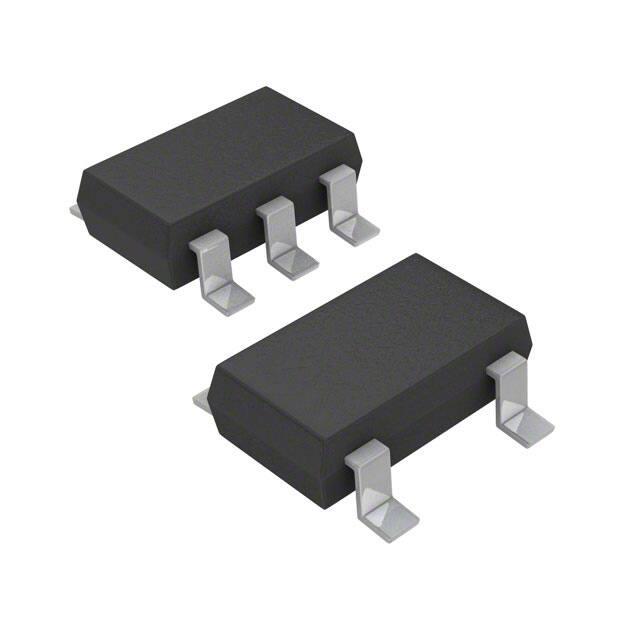
Tiny 5-Pin TSOT Package
Smallest External Components
bs
ol
et
e
The LX1995-x output current is
programmable using an external current
sense resistor in series with LEDs. This
configuration provides a feedback to the
FB pin which maintains constant output
current independent of input voltage
and LED forward voltage (VF). LED
dimming is accomplished using a PWM
signal or varying DC voltage methods.
The LX1995-x is available in the 5Pin TSOT and SOT-23 package. The
LX1995-1 can drive up to 6 LEDs
(switching current is 325mA). The
LX1995-2 can drive up to 10 LEDs
(switching current is 500mA).
WWW . Microsemi .C OM
The Microsemi LX1995-x is a
miniature LED driver with integrated
drivers. It is designed to drive white
or color LEDs in portable display
applications. The LX1995-x is an
adjustable step-up boost converter.
The LX1995-x can switch up to 2MHz
allowing designers to use a low cost,
small inductor and filter capacitor.
The driver supports a wide input
voltage range (1.6V to 5.5V) with
efficiency greater than 85% and can
start up at 1.6V input. The LX1995-x
is a low cost, high efficiency LED
driver. The design is based on a
pseudo-hysteretic pulse frequency
modulation topology.
In portable
battery applications the LX1995-x
offers high system efficiency with low
quiescent current: in operation IQ is <
70µA and in standby IQ is < 1µA.
APPLICATIONS
Pagers
Wireless Phones
PDAs
LED Driver
Digital Camera Displays
GPS Receivers
IMPORTANT: For the most current data, consult MICROSEMI’s website: http://www.microsemi.com
PRODUCT HIGHLIGHT
VBAT = 2.0V to 5.0V
SW
IN
LX1995
ON OFF
FB
SHDN
LX1995
O
GND
PACKAGE ORDER INFO
TA (°C)
Switch
Current
-40 to 85
-40 to 85
325mA
500mA
SG
Plastic TSOT
5-Pin
SE
Plastic SOT-23
5-Pin
RoHS Compliant / Pb-free
RoHS Compliant / Pb-free Transition DC: 0503
LX1995-1CSG
LX1995-2CSG
LX1995-1CSE
LX1995-2CSE
Note: Available in Tape & Reel. Append the letters “TR” to the part number. (i.e. LX1995-1CSG-TR)
Copyright © 2000
Rev. 1.1, 2005-07-07
Microsemi
Integrated Products Division
11861 Western Avenue, Garden Grove, CA. 92841, 714-898-8121, Fax: 714-893-2570
Page 1
�LX1995
®
TM
Miniature LED Driver
P RODUCTION D ATA S HEET
ABSOLUTE MAXIMUM RATINGS
PACKAGE PIN OUT
THERMAL DATA
GND
2
FB
3
5
IN
4
SHDN
SG PACKAGE
(Top View)
SW
1
GND
2
FB
3
5
IN
4
SHDN
SE PACKAGE
Plastic TSOT 5-Pin
(Top View)
THERMAL RESISTANCE-JUNCTION TO AMBIENT, θJA
SE
1
bs
ol
et
e
Note: Exceeding these ratings could cause damage to the device. All voltages are with respect to
Ground. Currents are positive into, negative out of specified terminal.
SG
SW
WWW . Microsemi .C OM
Supply Input Voltage ........................................................................-0.3V to 7.0V
Feedback Peak Pulse Input Voltage (VFB) ..............................-0.3V to VIN + 0.3V
Shutdown Input Voltage (V SHDN ) ...........................................-0.3V to VIN + 0.3V
Switch Voltage (VSW) ........................................................................-0.3V to 30V
Switch Current (ISW) ...................................................................................500mA
Operating Temperature Range .........................................................-40°C to 85°C
Maximum Operating Junction Temperature ................................................ 125°C
Storage Temperature Range...........................................................-65°C to 150°C
Peak Package Solder Reflow Temp. (40 second max. exposure) ... 260°C (+0, -5)
207°C/W
RoHS / Pb-free 100% Matte Tin Lead Finish
Plastic SOT-23 5-Pin
THERMAL RESISTANCE-JUNCTION TO AMBIENT, θJA
191°C/W
Junction Temperature Calculation: TJ = TA + (PD x θJA).
The θJA numbers are guidelines for the thermal performance of the device/pc-board system. All of the
above assume no ambient airflow.
FUNCTIONAL PIN DESCRIPTION
Name
SW
GND
Inductor Switching Connection – Internally connected to the drain of a 28V N-channel MOSFET. SW is high
impedance in shutdown.
Common terminal for ground reference.
Feedback Input – Connect to a current sense resistor between the load and GND to set the maximum output
current. FB pin is regulated to 320mV.
O
FB
Description
SHDN
Copyright © 2000
Rev. 1.1, 2005-07-07
Unregulated IC Supply Voltage Input – Input range from +2.0V to +5.5V. Bypass with a 1µF or greater capacitor
for low voltage operation.
Microsemi
Integrated Products Division
11861 Western Avenue, Garden Grove, CA. 92841, 714-898-8121, Fax: 714-893-2570
Page 2
PACKAGE DATA
IN
Active-Low Shutdown Input – A logic low shuts down the device and reduces the supply current to 10kHz
VPWM = 3.3V
DC = 10% to 90%
ILED = 0mA to 20mA
C2
R
3
90.9kΩ
R
2
11.2kΩ
0.1µF
R
1
15 Ω
Figure 4 – PWM to Analog Voltage Dimming LED Driver Application
L1
VBAT = 2.0V to 5.0V
10µH
1206 Case Size
C1
.1µF
SW
IN
LX1995
On
FB
320mV
SHDN
Off
2R - RA
VCC
RA
RCS
2R
LSB
VCC
MSB
R
RA = (0.64 x R) / VCC
MSB
LSB
ILED
1
1
1
0
0.50 x IMAX
0
1
0.75 x IMAX
0
0
APPLICATIONS
O
GND
Rcs = (0.32 x R) / {[R - (0.375 x RA)] x IMAX}
0.25 x IMAX
IMAX
Figure 5 – Binary Dimming LED Driver Application
The component values shown are only examples for a working system. Actual values will vary greatly depending on desired parameters, efficiency, and layout
constraints.
Copyright © 2000
Rev. 1.1, 2005-07-07
Microsemi
Integrated Products Division
11861 Western Avenue, Garden Grove, CA. 92841, 714-898-8121, Fax: 714-893-2570
Page 5
�LX1995
®
TM
Miniature LED Driver
P RODUCTION D ATA S HEET
THEORY OF OPERATION
bs
ol
et
e
R1 =
320mV
I LED( MAX)
eq. 1
O
⎛ R2 + R3 ⎞
⎛ R ⎞⎤
1 ⎡
⎟⎟ − VADJ ⋅ ⎜⎜ 2 ⎟⎟⎥
⎢320mV ⋅ ⎜⎜
R1 ⎣⎢
R
3
⎝
⎠
⎝ R 3 ⎠⎦⎥
Copyright © 2000
Rev. 1.1, 2005-07-07
eq. 2
OUTPUT RIPPLE AND CAPACITOR SELECTION
Output voltage ripple is depended on the selection of the
inductor value (L), output capacitor value (COUT), peak
switch current (IPEAK), load current (IOUT), input voltage
(VIN) and the output voltage (VOUT). The peak-to-peak
voltage ripple is a function of the output droop (as the
inductor current charges to IPEAK), the feedback transition
error (i.e., typically 10mV), and the output overshoot
(energy stored in the inductor). When the switch is first
turn on, the total ripple voltage is:
VRIPPLE = ∆VDROOP + ∆VOVERSHOOT+ 10mV
eq. 3
The initial droop can be estimated with the assumption
of 0.5V of voltage drop across the inductor and FET
RDSON.
⎛ L ⎞
⎟ ⋅ (IPK × ILED )
⎜⎜
COUT ⎟⎠
⎝
∆VDROOP =
VIN − 0.5
eq. 4
The output overshoot calculated with 0.5V as voltage
drop across the diode.
1 ⎛ L ⎞
⎟⎟ ⋅ (IPK − ILED )2
⋅ ⎜⎜
2 C
∆VOVERSHOOT = ⎝ OUT ⎠
VOUT − VIN + 0.5
eq. 5
Once the output voltage ripple is determined for the
selected components, the output capacitor can then be
adjusted to meet the target ripple voltage requirements.
The LX1995-x is targeted for LED driver applications;
output voltage ripple is not a critical application
requirement.
Microsemi
Integrated Products Division
11861 Western Avenue, Garden Grove, CA. 92841, 714-898-8121, Fax: 714-893-2570
Page 6
APPLICATIONS
DIMMING METHODS
LX1995-x supports two dimming methods: PWM or DC
Voltage.
PWM mode: Connect system PWM logic signal to the
SHDN pin (See Figure 1). This turns the LX1995-X on and
off which pulses the LED current between zero and the
setting determined by R1.
DC Voltage mode: The designer can apply an adjustable
DC voltage supply to the FB pin. As the DC voltage
increases, the LED current decreases. The equation (see
Figure 3) is:
I LED =
INDUCTOR SELECTION AND OUTPUT CURRENT LIMIT
PROGRAMMING
Microsemi recommends the use inductors (for the
LX1995-1) in the range of 10µH to 47µH due to saturation
of peak inductor current. By increasing the average
inductor current, the LX1995-x will extend the power
range. Smaller inductor values will reduce output voltage
ripple and are smaller in size.
WWW . Microsemi .C OM
OPERATING THEORY
The LX1995-x is a PFM boost converter optimized for
driving a series of white or color LEDs. It operates in a
pseudo-hysteretic mode with a fixed, 300ns, switch “off
time”. When the LX1995-x enables, the LED current
decreases causing the FB voltage to decrease to a value less
than 320mV. The feedback comparator (See Simplified
Block Diagram) activates the control logic. The control
logic turns on the DRV output circuit that connects to the
internal N-Channel MOSFET gate. The switch output
(SW) is switched “on” and remains “on” until the inductor
current ramps up to the peak current level (typically 325mA
for LX1995-1).
The LED load is powered from energy stored in the
output capacitor during the inductor charging cycle. Once
the peak inductor current value is achieved, the output is
turned off and the energy stored in the inductor delivers to
the load. This causes the voltage to rise across the current
setting resistor (R1) at the input to the feedback circuit. The
LX1995-x continues to switch until the voltage at the FB
pin exceeds 320mV. The value of R1 is calculated by
dividing 320mV by the maximum series LED current. A
minimum value of 3.3Ω is recommended for RSET. The
voltage at the FB pin is the product of the LED current
(ILED) and R1.
�LX1995
®
TM
Miniature LED Driver
P RODUCTION D ATA S HEET
LX1995-2 EFFICIENCY
100
90
90
Efficiency
100
80
5.0V IN
70
3.5V IN
WWW . Microsemi .C OM
Efficiency
LX1995-1 EFFICIENCY
80
5.0V IN
70
60
bs
ol
et
e
3.5V IN
60
47µH Inductor, 4 White LEDs
50
47µH Inductor, 4 White LEDs
50
2
4
6
8
10
12
14
16
18
20
4
6
8
10
12
14
16
18
20
LED Current
O
LED Current
2
CHARTS
Copyright © 2000
Rev. 1.1, 2005-07-07
Microsemi
Integrated Products Division
11861 Western Avenue, Garden Grove, CA. 92841, 714-898-8121, Fax: 714-893-2570
Page 7
�LX1995
®
TM
Miniature LED Driver
P RODUCTION D ATA S HEET
PACKAGE DIMENSIONS
WWW . Microsemi .C OM
SG
5-Pin Thin Shrink Small Outline Package (TSOT)
e
3
2
1
E1
4
5
b
e1
D
A2
A
MILLIMETERS
MIN
MAX
1.00
0.01
0.10
0.84
0.90
0.30
0.45
0.12
0.20
2.90 BSC
2.80 BSC
1.60 BSC
0.95 BSC
0.30
0.40
0.25 BSC
INCHES
MIN
MAX
0.039
0.0004 0.004
0.033
0.035
0.012
0.018
0.005
0.008
0.114 BSC
0.110 BSC
0.063 BSC
0.037 BSC
0.012
0.016
0.010 BSC
Dim
A
A1
B
C
D
E
F
G
H
I
J
K
MILLIMETERS
MIN
MAX
0.90
1.30
0.90
1.45
0.25
0.50
0.09
0.20
2.80
3.10
1.50
1.75
0.95 BSC
1.90 BSC
2.60
3.00
0.35
0.55
0.00
0.15
10° MAX
INCHES
MIN
MAX
0.035
0.051
0.035
0.057
0.010
0.020
0.004
0.008
0.110
0.122
0.059
0.069
0.038 BSC
0.075 BSC
0.102
0.118
0.014
0.022
0.000
0.006
10° MAX
bs
ol
et
e
E
Dim
A
A1
A2
b
C
D
E
E1
e
L
L2
A1
L2
L
C
SE
5-Pin Small Outline Package (SOT-23)
D
G
H
A
A1
B
Note:
F
J
C
I
K
MECHANICALS
O
E
Dimensions do not include mold flash or protrusions; these shall not exceed 0.155mm(.006”) on any side. Lead dimension shall
not include solder coverage.
Copyright © 2000
Rev. 1.1, 2005-07-07
Microsemi
Integrated Products Division
11861 Western Avenue, Garden Grove, CA. 92841, 714-898-8121, Fax: 714-893-2570
Page 8
�LX1995
®
TM
Miniature LED Driver
P RODUCTION D ATA S HEET
NOTES
O
bs
ol
et
e
WWW . Microsemi .C OM
NOTES
PRODUCTION DATA – Information contained in this document is proprietary to
Microsemi and is current as of publication date. This document may not be modified in
any way without the express written consent of Microsemi. Product processing does not
necessarily include testing of all parameters. Microsemi reserves the right to change the
configuration and performance of the product and to discontinue product at any time.
Copyright © 2000
Rev. 1.1, 2005-07-07
Microsemi
Integrated Products Division
11861 Western Avenue, Garden Grove, CA. 92841, 714-898-8121, Fax: 714-893-2570
Page 9
�


 工商网监
湘ICP备2023018690号
工商网监
湘ICP备2023018690号
