LX5255
INTEGRATED PRODUCTS
9-Line LVD SCSI Terminator
P R ODUCTION
DATA SHEET
DESCRIPTION
KEY FEATURES
W WW . Microsemi . C OM
The LX5255 is a Low Voltage Differential (LVD) terminator designed to comply with the LVD termination specification in the SPI-4 document. The LX5255 is specifically designed for LVD only applications. Because the LX5255 supports only LVD, it has lower output capacitance than multimode terminators such as the LX5250. The LX5255 utilizes an industry standard LVD architecture. The individual high bandwidth drivers maximize channel separation, reduce channel-to-channel noise and cross talk to insure Ultra320 performance. When the LX5255 is enabled, the Differential Sense (DIFSENS) pin
supplies a voltage between 1.2V and 1.4V. In application, the terminator DIFFB input is connected to the system DIFSENS line. If there are no single ended or High Voltage Differential (HVD) devices attached to the system, the LVD output will be enabled. If the DIFSENS line is LOW, indicating a single ended device, the LX5255 output will be HiZ. If the DIFSENS line is HIGH, indicating a HVD device, the LX5255 output will be HiZ. The LX5255 has a TTL compatible sleep/disable mode. Applying a logic HIGH to the DISC pin puts the LX5255 in sleep mode. During sleep mode, power dissipation is reduced to a meager 5µA while also placing all outputs and the DIFSENS function in a HiZ state.
Compliant with SPI-2 (Ultra2), SPI-3 (Ultra160), and SPI-4 (Ultra320) 2.5pF Maximum Disabled Output Capacitance Fast Response, No External Capacitors Required 5µA Supply Current in Disconnect Mode 30mA Supply During Normal Operation Logic Command Disconnects All Termination Lines DIFSENS Line Driver Current Limit and Thermal Protection Pin Compatible With Unitrode UCC5640
IMPORTANT: For the most current data, consult MICROSEMI’s website: http://www.microsemi.com
TYPICAL APPLICATION
+
L X 5255
+
L X 5255
LX5255 Typical Application
LX5255 LX5255
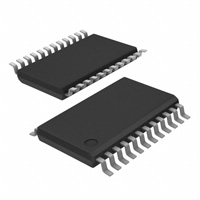
PACKAGE ORDER INFO TSSOP TA (°C) PW 24-Pin 0 to 70 LX5255CPW
Note: Available in Tape & Reel. Append the letter “T” to the part number. (i.e. LX5255CPWT)
Copyright 2000 Rev. 1.0a, 2003-06-30
Microsemi
Integrated Products Division 11861 Western Avenue, Garden Grove, CA. 92841, 714-898-8121, Fax: 714-893-2570
Page 1
�LX5255
INTEGRATED PRODUCTS
9-Line LVD SCSI Terminator
P R ODUCTION
DATA SHEET
ABSOLUTE MAXIMUM RATINGS Term Power (VTERM)............................................................................................-0.3V to 7V Signal Line Voltage .............................................................................................-0.3V to 7V Differential Voltage .............................................................................................-0.3V to 7V Operating Junction Temperature.................................................................................. 150°C Storage Temperature Range........................................................................... -65°C to 150°C Lead Temperature (Soldering 10 seconds)................................................................... 300°C
Note: Exceeding these ratings could cause damage to the device. All voltages are with respect to Ground. Currents are positive into, negative out of specified terminal.
PACKAGE PIN OUT
W WW . Microsemi . C OM
NC 1+ 12+ 23+ 34+ 4DIFFB DIFSENS GND
1 2 3 4 5 6 7 8 9 10 11 12
24 23 22 21 20 19 18 17 16 15 14 13
VTERM 99+ 88+ 77+ 66+ 55+ DISC
THERMAL DATA
PW
24L TSSOP 100°C/W
PW PACKAGE (Top View) NC – No Internal Connection
THERMAL RESISTANCE-JUNCTION TO AMBIENT, θJA
Junction Temperature Calculation: TJ = TA + (PD x θJA). The θJA numbers are guidelines for the thermal performance of the device/pc-board system. All of the above assume no ambient airflow. θJA can vary significantly depending on mounting technique. (See Application Notes Section: Thermal considerations)
DIFFB/POWER UP/POWER DOWN FUNCTION TABLE DISC DIFFB Outputs Status
Disable Enable Disable Disable
Type
HI-Z LVD HI-Z HI-Z
Quiescent Current
8mA 30mA 8mA 10µA
L L L H or Open
L < 0.5V 0.7V to 1.9V H > 2.4V X
RECOMMENDED MAX OPERATING CONDITIONS Parameter
VTerm Signal Line Voltage Disconnect Input Voltage Operating Junction Temperature TJ
Symbol
VTERM
Min
2.7 0 0 0
LX5255 Typ
Max
5.25 5.0 VTERM 70
Units
PACKAGE DATA PACKAGE DATA
V V V °C
Copyright 2000 Rev. 1.0a, 2003-06-30
Microsemi
Integrated Products Division 11861 Western Avenue, Garden Grove, CA. 92841, 714-898-8121, Fax: 714-893-2570
Page 2
�LX5255
INTEGRATED PRODUCTS
9-Line LVD SCSI Terminator
P R ODUCTION
DATA SHEET
Unless otherwise specified, the following specifications apply over the operating ambient temperature 0°C ≤ TA ≤ 70°C, VTerm = 3.3V, and DISCONNECT = 0V. LX5255 Parameter Symbol Test Conditions Units Min Typ Max
LVD Terminator Section VTerm Supply Current Common Mode Voltage Offset Voltage (Note 1) Differential Terminator Impedance Common Mode Impedance Output Capacitance (Note 2) Mode Change Delay DIFSENS Section DIFSENS Output Voltage DIFSENS Output Source Current DIFSENS Sink Current Disconnect Section Disconnect Threshold Input Current Note 1: Open Circuit failsafe voltage. Note 2: Guaranteed by design. VTH IIH DISCONNECT = 0V 0.8 2.0 10 V µA VDIFF IDIFF ISINK(DIFF) DIFSENS = 0V VTERM = 2.75V 1.2 5 20 1.3 1.4 15 200 V mA µA ICC VCM VOS ZD ZCM CO tDF Open circuit between (-) and (+) terminals VOUT Differential = -1V to +1V 0.5V to 2V DISCONNECT > 2.0V DIFSENS = 1.4V to 0V 100 115 All term lines open DISCONNECT > 2.0V 1.125 100 100 110 30 5 1.25 112 105 150 35 20 1.375 125 110 190 3 300 mA µA V mV Ω Ω pF ms
ELECTRICAL CHARACTERISTICS
W WW . Microsemi . C OM
ELECTRICALS ELECTRICALS
Copyright 2000 Rev. 1.0a, 2003-06-30
Microsemi
Integrated Products Division 11861 Western Avenue, Garden Grove, CA. 92841, 714-898-8121, Fax: 714-893-2570
Page 3
�LX5255
INTEGRATED PRODUCTS
9-Line LVD SCSI Terminator
P R ODUCTION
DATA SHEET
BLOCK DIAGRAM
W WW . Microsemi . C OM
VTERM
24
DISC 1.07 mA
1 of 9 Lines
HVD LVD SE
DISC
13
3
LVD(-)
52.5 150 HVD 52.5 1.25V 1.07 mA LVD SE 10mA I-Limited 1.3V Source D IFSENS DIFFB
2
LVD(+)
12
DISC + SE HVD LATCH
Window Comp.
GND
11 10
LVD POWER ON & MODE DELAY
Figure 1 – LX5255CPW Block Diagram
FUNCTIONAL PIN DESCRIPTION PIN NAME 1-, 2-, 3-, 4-, 5-, 6-, 7-, 8-, 91+, 2+, 3+, 4+, 5+, 6+, 7+, 8+, 9+ DESCRIPTION Negative signal termination lines for LVD mode. Positive signal termination lines for LVD mode.
Power supply pin for terminator. Connect to SCSI bus VTERM. Must be decoupled by one 4.7µF low-ESR capacitor for every three terminator devices. It is
VTERM absolutely necessary to connect this pin to the decoupling capacitor through a very low impedance (big traces to PCB). Keeping distances very short from the decoupling capacitors is somewhat layout dependent and some applications may benefit from high frequency decoupling with 0.1µF capacitors at VTERM pin.
PACKAGE DATA PACKAGE DATA
DISC GND DIFSENS DIFFB
5
Enables/Disables terminator. See Power Down Function Table for logic levels.
Terminator ground pin. Connect to ground. Differential sense pin connected to system DIFFSENS line. Drives the SCSI bus DIFSENS line to 1.3V. Used to detect the SCSI bus mode (SE, LVD or HVD). Should be connected to a 4.7uF capacitor to GND, and a 50KΩ resistor to the DIFFSENS pin (see Figure 2 on page 5).
Copyright 2000 Rev. 1.0a, 2003-06-30
Microsemi
Integrated Products Division 11861 Western Avenue, Garden Grove, CA. 92841, 714-898-8121, Fax: 714-893-2570
Page 4
�LX5255
INTEGRATED PRODUCTS
9-Line LVD SCSI Terminator
P R ODUCTION
DATA SHEET
APPLICATION
PERIPHERAL
11+ Data Lines (9) 99+ 99+ 11+ VTERM
W WW . Microsemi . C OM
HOST
TERMPOWER VTERM
TERMPOWER
DISCONNECT
LX5255
DISC GND
LX5255
DISC GND
DISCONNECT
NC* 4.7uF 4.7uF
DIFSENS DIFFB
Pin 1
DIFSENS DIFFB 50k 50k 4.7uF
Pin 1
NC* 4.7uF 4.7uF
4.7uF
VTERM
11+ Data Lines (9) 99+
11+ 99+
VTERM
LX5255
DISC GND
LX5255
DISC GND
DIFSENS NC* 4.7uF
Pin 1
DIFFB
DIFSENS DIFFB
Pin 1
NC* 4.7uF
VTERM
11+ Control Lines (9) 99+
11+ 99+
VTERM
LX5255
DISC GND
LX5255
DISC GND
DIFSENS NC* 4.7uF
Pin 1
DIFFB
DIFSENS DIFFB
Pin 1
NC* 4.7uF
APPLICATIONS APPLICATIONS
* The capacitor on Pin 1 can be placed on the LX5255PCW to be pin compatible with other devices. This capacitor is not required.
Figure 2 – Suggested Microsemi LX5255 Universal Application Schematic
Copyright 2000 Rev. 1.0a, 2003-06-30
Microsemi
Integrated Products Division 11861 Western Avenue, Garden Grove, CA. 92841, 714-898-8121, Fax: 714-893-2570
Page 5
�LX5255
INTEGRATED PRODUCTS
9-Line LVD SCSI Terminator
P R ODUCTION
DATA SHEET
MECHANICAL DRAWINGS
W WW . Microsemi . C OM
PW
24-Pin Thin Small Shrink Outline (TSSOP)
321 E P
F D AH
SEATING PLANE
B
G
L
INCHES MIN MAX 0.033 0.037 0.007 0.012 0.0035 0.008 0.303 0.311 0.169 0.177 0.025 BSC 0.002 0.005 – .0433 0.020 0.030 0° 8° 0.246 0.256 – 0.004
C
M
Dim A B C D E F G H L M P *LC
Note:
MILLIMETERS MIN MAX 0.85 0.95 0.19 0.30 0.09 0.20 7.70 7.90 4.30 4.50 0.65 BSC 0.05 0.15 – 1.10 0.50 0.75 0° 8° 6.25 6.50 – 0.10
MECHANICALS MECHANICALS
1. Dimensions do not include mold flash or protrusions; these shall not exceed 0.155mm(.006”) on any side. Lead dimension shall not include solder coverage.
Copyright 2000 Rev. 1.0a, 2003-06-30
Microsemi
Integrated Products Division 11861 Western Avenue, Garden Grove, CA. 92841, 714-898-8121, Fax: 714-893-2570
Page 6
�LX5255
INTEGRATED PRODUCTS
9-Line LVD SCSI Terminator
P R ODUCTION
DATA SHEET
NOTES
W WW . Microsemi . C OM
NOTES NOTES
PRODUCTION DATA – Information contained in this document is proprietary to Microsemi and is current as of publication date. This document may not be modified in any way without the express written consent of Microsemi. Product processing does not necessarily include testing of all parameters. Microsemi reserves the right to change the configuration and performance of the product and to discontinue product at any time.
Copyright 2000 Rev. 1.0a, 2003-06-30
Microsemi
Integrated Products Division 11861 Western Avenue, Garden Grove, CA. 92841, 714-898-8121, Fax: 714-893-2570
Page 7
�