L I N D O C # : 8384
LX8384-xx/8384A-xx/8384B-xx
5 A L OW D ROPOUT P OSITIVE R E G U L AT O R S
T
HE
I
NFINITE
P
OWER
OF
I
N N O VAT I O N
P
RODUCTION
D
ATA
S
HEET
DESCRIPTION The LX8384/84A/84B Series ICs are positive regulators designed to provide 5A output current. These regulators yield higher efficiency than currently available devices with all internal circuitry designed to operate down to a 1V input-to-output differential. In each of these products, the dropout voltage is fully specified as a function of load current. Dropout is guaranteed at a maximum of 1.3V (8384A) and 1.5V (8384) at maximum output current, decreasing at lower load currents. In addition, on-chip trimming adjusts the reference voltage tolerance to 1% maximum at room temperature and 2% maximum over the 0 to 125°C range for the LX8384A, making this ideal for the Pentium P54C-VRE specification. The LX8384B offers 0.8% tolerance at room temperature and 1.0% maximum over line, load and temperature. Fixed versions are also available and specified in the Available Options table below. The LX8384/84A/84B Series devices are pin-compatible with earlier 3terminal regulators, such as the 117 series products. While a 10µF output capacitor is required on both input and output of these new devices, this capacitor is generally included in most regulator designs. The LX8384/84A/84B Series quiescent current flows into the load, thereby increasing efficiency. This feature constrasts with PNP regulators where up to 10% of the output current is wasted as quiescent current. The LX8384-xxI is specified over the industrial temperature range of -25°C to 125°C, while the LX8384-xxC/84A-xxC/84B-xxC is specified over the commercial range of 0°C to 125°C.
K E Y F E AT U R E S
s THREE-TERMINAL ADJUSTABLE OR FIXED OUTPUT s GUARANTEED < 1.3V HEADROOM AT 5A (LX8384A-xx) s GUARANTEED 2.0% MAX. REFERENCE TOLERANCE (LX8384A-xx) s GUARANTEED 1.0% MAX. REFERENCE TOLERANCE (LX8384B-xx) s OUTPUT CURRENT OF 5A MINIMUM p 0.015% LINE REGULATION p 0.15% LOAD REGULATION
A P P L I C AT I O N S
s PENTIUM® PROCESSOR VRE APPLICATIONS s HIGH EFFICIENCY LINEAR REGULATORS s POST REGULATORS FOR SWITCHING POWER SUPPLIES s BATTERY CHARGERS s CONSTANT CURRENT REGULATORS s CYRIX® 6x86TM s AMD-K5 TM
IMPORTANT: For the most current data, consult LinFinity's web site: http://www.linfinity.com.
PRODUCT HIGHLIGHT
A VA I L A B L E O P T I O N S
Part #
LX8384/84A/84B-00 LX8384/84A/84B-15 LX8384/84A/84B-33
PER
PAR T #
Output Voltage
3.5V, 5A R E G U L AT O R
Adjustable 1.5V 3.3V
5V
IN
LX8384A
ADJ
OUT 121Ω 0.1%
3.5V at 5A 1500µF* 5x 6MV1500GX Sanyo
*1500µF
6MV1500GX Sanyo
Other voltage options may be available — Please contact factory for details.
218Ω 0.1%
* Capacitors mustotal ESR. have < 20mΩ T
An application of the LX8384A for the Pentium P54C processors meeting VRE specfication. PA C K A G E O R D E R I N F O R M AT I O N TA (°C) Max. Ref. Max. Dropout Accuracy Voltage 2.0% 0 to 125 -25 to 125 2.0% 1.0% 2.0% 1.5V 1.3V 1.3V 1.5V
P Plastic TO-220 3-pin
LX8384-xxCP LX8384A-xxCP LX8384B-xxCP LX8384-xxIP
DD Plastic TO-263 3-pin
LX8384-xxCDD LX8384A-xxCDD LX8384B-xxCDD LX8384-xxIDD
Note: All surface-mount packages are available in Tape & Reel, append the letter "T" to part number. (i.e. LX8384A-xxCDDT) "xx" refers to output voltage, please see table above.
Copyright © 1997 Rev. 1.9 12/97
LINFINITY MICROELECTRONICS INC.
11861 W ESTERN A VENUE, G ARDEN G ROVE, CA. 92841, 714-898-8121, F AX: 714-893-2570
1
�PRODUCT DATABOOK 1996/1997
LX8384-xx/8384A-xx/8384B-xx
5 A L O W D R O P O U T P O S I T I V E R E G U L AT O R S
P
RODUCTION
D
ATA
S
HEET
A B S O LUT E M AXIM UM R ATINGS
(Note 1)
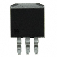
PACKAGE PIN OUTS
TAB IS V OUT
3 2 1
Power Dissipation .................................................................................. Internally Limited Input Voltage ................................................................................................................ 10V Input to Output Voltage Differential ........................................................................... 10V Operating Junction Temperature Hermetic (K - Package) ........................................................................................ 150°C Plastic (DD - Package) .......................................................................................... 150°C Storage Temperature Range ...................................................................... -65°C to 150°C Lead Temperature (Soldering, 10 seconds) ............................................................. 300°C
Note 1. Exceeding these ratings could cause damage to the device. All voltages are with respect to Ground. Currents are positive into, negative out of the specified terminal.
VIN VOUT ADJ / GND*
P PACKAGE (Top View)
* Pin 1 is GND for fixed voltage versions.
TAB IS V OUT
T H E R M A L D ATA
3
VIN VOUT ADJ / GND*
P PACKAGE: THERMAL RESISTANCE-JUNCTION TO TAB, θJT THERMAL RESISTANCE-JUNCTION TO AMBIENT, θ JA DD PACKAGE: THERMAL RESISTANCE-JUNCTION TO TAB, θJT THERMAL RESISTANCE-JUNCTION TO AMBIENT, θ JA 2.7°C/W 60°C/W* 2.7°C/W 60°C/W
2 1
DD PACKAGE (Top View)
* Pin 1 is GND for fixed voltage versions.
Junction Temperature Calculation: TJ = TA + (PD x θJA). The θ JA numbers are guidelines for the thermal performance of the device/pc-board system. All of the above assume no ambient airflow. * θ JAcan be improved with package soldered to 0.5IN2 copper area over backside ground plane or internal power plane. θJAcan vary from 20ºC/W to > 40ºC/W depending on mounting technique.
BLOCK DIAGRAM
VIN
Bias Circuit Thermal Limit Circuit Bandgap Circuit Control Circuit Output Circuit
VOUT
SOA Protection Circuit
ADJ or GND*
* This pin GND for fixed voltage versions.
Current Limit Circuit
2
Copyright © 1997 Rev. 1.9 12/97
�PRODUCT DATABOOK 1996/1997
LX8384-xx/8384A-xx/8384B-xx
5 A L OW D ROPOUT P OSITIVE R E G U L AT O R S
P
RODUCTION
D
ATA
S
HEET
ELECTRICAL CHARACTERISTICS
(Unless otherwise specified, these specifications apply over the operating ambient temperatures for the LX8384-xxC/8384A-xxC/8384B-xxC with 0°C ≤ T A ≤ 125°C, and the LX8384-xxI with -25°C ≤ TA ≤ 125°C; VIN - VOUT = 3V; IOUT = 5A. Low duty cycle pulse testing techniques are used which maintains junction and case temperatures equal to the ambient temperature.)
LX8384-00 / 8384A-00 / 8384B-00 (Adjustable)
Parameter
Reference Voltage (Note 4) LX8384/84A-00
Symbol
VREF
Test Conditions
LX8384/84A/84B-00 Min. Typ. Max.
1.238 1.225 1.240 1.238 1.250 1.250 1.250 1.250 0.015 0.035 0.15 0.01 83 55 0.2 1.2 1.1 2 6 4 0.25 0.3 0.003 1.262 1.270 1.260 1.262 0.2 0.3 0.5 0.02
Units
V V V V % % % %/W dB µA µA V V mA A A % % %
IOUT = 10mA, TA = 25°C 10mA ≤ IOUT ≤ 5A, 1.5V ≤ (VIN - VOUT), VIN ≤ 10V, P ≤ PMAX LX8384B-00 IOUT = 10mA, TA = 25°C 10mA ≤ IOUT ≤ 5A, 1.5V ≤ (VIN - VOUT), VIN ≤ 10V, P ≤ PMAX Line Regulation (Note 2) ∆V REF 1.3V ≤ (VIN - V OUT), VIN ≤ 7V, IOUT = 10mA (VIN ) 1.3V ≤ (VIN - VOUT ), VIN ≤ 10V, IOUT = 10mA ∆VREF (IOUT) VOUT ≥ V REF, VIN - VOUT = 3V, 10mA ≤ IOUT ≤ 5A Load Regulation (Note 2) Thermal Regulation ∆VOUT (Pwr) TA = 25°C, 20ms pulse Ripple Rejection (Note 3) VOUT = 5V, f =120Hz, COUT = 100µf Tantalum, VIN = 6.5V CADJ = 10µF, I OUT = 5A Adjust Pin Current I ADJ Adjust Pin Current Change (Note 4) ∆IADJ 10mA ≤ IOUT ≤ IOUT (MAX) , 1.3V ≤ (VIN - VOUT), VIN ≤ 10V Dropout Voltage LX8384-00 ∆V ∆VREF = 1%, IOUT = 5A LX8384A/84B-00 ∆VREF = 1%, IOUT = 5A Minimum Load Current IOUT (MIN) VIN ≤ 10V Maximum Output Current IOUT (MAX) (VIN - VOUT) ≤ 7V (VIN - VOUT) ≤ 10V Temperature Stability (Note 3) ∆VOUT (T) Long Term Stability (Note 3) ∆VOUT (t) TA = 125°C, 1000 hours RMS Output Noise (% of VOUT) (Note 3) VOUT (RMS) TA = 25°C, 10Hz ≤ f ≤ 10kHz
65 20
100 5 1.5 1.3 10
5 3
1
LX8384-15 / 8384A-15 / 8384B-15 (1.5V Fixed)
Parameter
Output Voltage (Note 4) LX8384/84A-15
Symbol
VOUT
Test Conditions
LX8384/84A/84B-15 Min. Typ. Max.
1.485 1.470 1.488 1.485 1.50 1.50 1.50 1.50 1 1 2.5 0.01 83 4 1.2 1 6 0.25 0.3 0.003 1.515 1.530 1.512 1.515 3 5 7 0.02 10 1.5 1.3
Units
V V V V mV mV mV %/W dB mA V V A % % %
VIN = 5V, IOUT = 0mA, TA = 25°C 4.75V ≤ V IN ≤ 10V, 0mA ≤ IOUT ≤ 5A, P ≤ PMAX LX8384B-15 VIN = 5V, IOUT = 0mA, TA = 25°C 4.75V ≤ V IN ≤ 10V, 0mA ≤ IOUT ≤ 5A, P ≤ PMAX Line Regulation (Note 2) ∆VOUT 4.75V ≤ V IN ≤ 7V (VIN ) 4.75V ≤ VIN ≤ 10V Load Regulation (Note 2) ∆VOUT (IOUT) VIN = 5V, 0mA ≤ IOUT ≤ IOUT (MAX) Thermal Regulation ∆VOUT (Pwr) TA = 25°C, 20ms pulse Ripple Rejection (Note 3) COUT = 100µF (Tantalum), IOUT = 5A Quiescent Current IQ 0mA ≤ IOUT ≤ IOUT (MAX) , 4.75V ≤ VIN ≤ 10V Dropout Voltage LX8384-15 ∆V ∆VOUT = 1%, IOUT ≤ IOUT (MAX) LX8384A/84B-15 ∆VOUT = 1%, IOUT ≤ IOUT (MAX) Maximum Output Current IOUT (MAX) VIN ≤ 7V Temperature Stability (Note 3) ∆VOUT (T) Long Term Stability (Note 3) ∆VOUT (t) TA = 125°C, 1000 hours RMS Output Noise (% of VOUT) (Note 3) VOUT (RMS) TA = 25°C, 10Hz ≤ f ≤ 10kHz
60
5
1
Note 2. Regulation is measured at constant junction temperature, using pulse testing with a low duty cycle. Changes in output voltage due to heating effects are covered under the specification for thermal regulation. Note 3. These parameters, although guaranteed, are not tested in production. Note 4. See Maximum Output Current Section above.
Copyright © 1997 Rev. 1.9 12/97
3
�PRODUCT DATABOOK 1996/1997
LX8384-xx/8384A-xx/8384B-xx
5 A L O W D R O P O U T P O S I T I V E R E G U L AT O R S
P
RODUCTION
D
ATA
S
HEET
ELECTRICAL CHARACTERISTICS
(Continued)
LX8384-33 / 8384A-33 / 8384B-33 (3.3V Fixed)
Parameter
Output Voltage (Note 4) LX8384/84A-33
Symbol
VOUT
Test Conditions
LX8384/84A/84B-33 Min. Typ. Max.
3.267 3.235 3.274 3.267 3.30 3.30 3.30 3.30 1 2 5 0.01 83 4 1.2 1 6 0.25 0.3 0.003 3.333 3.365 3.326 3.333 6 10 15 0.02 10 1.5 1.3
Units
V V V V mV mV mV %/W dB mA V V A % % %
VIN = 5V, IOUT = 0mA, TA = 25°C 4.75V ≤ V IN ≤ 10V, 0mA ≤ IOUT ≤ 5A, P ≤ PMAX LX8384B-33 VIN = 5V, IOUT = 0mA, TA = 25°C 4.75V ≤ V IN ≤ 10V, 0mA ≤ IOUT ≤ 5A, P ≤ PMAX Line Regulation (Note 2) ∆VOUT 4.75V ≤ VIN ≤ 7V (VIN ) 4.75V ≤ VIN ≤ 10V Load Regulation (Note 2) ∆VOUT (IOUT) VIN = 5V, 0mA ≤ IOUT ≤ IOUT (MAX) Thermal Regulation ∆VOUT (Pwr) TA = 25°C, 20ms pulse Ripple Rejection (Note 3) COUT = 100µF (Tantalum), IOUT = 5A Quiescent Current IQ 0mA ≤ IOUT ≤ IOUT (MAX) , 4.75V ≤ VIN ≤ 10V Dropout Voltage LX8384-33 ∆V ∆VOUT = 1%, IOUT ≤ IOUT (MAX) LX8384A/84B-33 ∆VOUT = 1%, IOUT ≤ IOUT (MAX) Maximum Output Current IOUT (MAX) VIN ≤ 7V Temperature Stability (Note 3) ∆VOUT (T) Long Term Stability (Note 3) ∆VOUT (t) TA = 125°C, 1000 hours RMS Output Noise (% of VOUT) (Note 3) VOUT (RMS) TA = 25°C, 10Hz ≤ f ≤ 10kHz
60
5
1
4
Copyright © 1997 Rev. 1.9 12/97
�PRODUCT DATABOOK 1996/1997
LX8384-xx/8384A-xx/8384B-xx
5 A L OW D ROPOUT P OSITIVE R E G U L AT O R S
P
RODUCTION
D
ATA
S
HEET
A P P L I C AT I O N N O T E S The LX8384/84A/84B Series ICs are easy to use Low-Dropout (LDO) voltage regulators. They have all of the standard self-protection features expected of a voltage regulator: short circuit protection, safe operating area protection and automatic thermal shutdown if the device temperature rises above approximately 165°C. Use of an output capacitor is REQUIRED with the LX8384/84A/ 84B series. Please see the table below for recommended minimum capacitor values. These regulators offer a more tightly controlled reference voltage tolerance and superior reference stability when measured against the older pin-compatible regulator types that they replace. STABILITY The output capacitor is part of the regulator’s frequency compensation system. Many types of capacitors are available, with different capacitance value tolerances, capacitance temperature coefficients, and equivalent series impedances. For all operating conditions, connection of a 220µF aluminum electrolytic capacitor or a 47µF solid tantalum capacitor between the output terminal and ground will guarantee stable operation. If a bypass capacitor is connected between the output voltage adjust (ADJ) pin and ground, ripple rejection will be improved (please see the section entitled “RIPPLE REJECTION”). When ADJ pin bypassing is used, the required output capacitor value increases. Output capacitor values of 220µF (aluminum) or 47µF (tantalum) provide for all cases of bypassing the ADJ pin. If an ADJ pin bypass capacitor is not used, smaller output capacitor values are adequate. The table below shows recommended minimum capacitance values for stable operation. RECOMMENDED CAPACITOR VALUES INPUT
10µF 10µF
Power Supply IN
LX8384/84A OUT /84B
ADJ
Minumum Load (Larger resistor) Full Load (Smaller resistor) RDSON