LIN D O C # : 8386
LX8386-xx/8386A-xx/8386B-xx
1 . 5 A LOW DR O P O U T P OSITIVE R E G U L AT O R S
T
H E
I
N F I N I T E
P
O W E R
O F
I
N N O VA T I O N
P
DESCRIPTION
The LX8386/86A/86B series ICs are
positive regulators designed to provide
1.5A output current. These regulators
yield higher efficiency than currently
available devices with all internal
circuitry designed to operate down to a
1V input-to-output differential. In this
product, the dropout voltage is fully
specified as a function of load current.
Dropout is guaranteed at a maximum of
1.3V (LX8386A/86B) and 1.5V (LX8386)
at maximum output current, decreasing
at lower load currents. On-chip
trimming adjusts the reference voltage
to 1% (0.8% for the 8386B) initial
accuracy and 2% (1% for the 8386B)
over line, load and temperature.
The LX8386/86A/86B series devices
D
R O D U C T I O N
A T A
S
H E E T
K E Y F E AT U R E S
■ Three-Terminal Adjustable or Fixed
Output
■ Guaranteed 40ºC/W depending on
mounting technique.
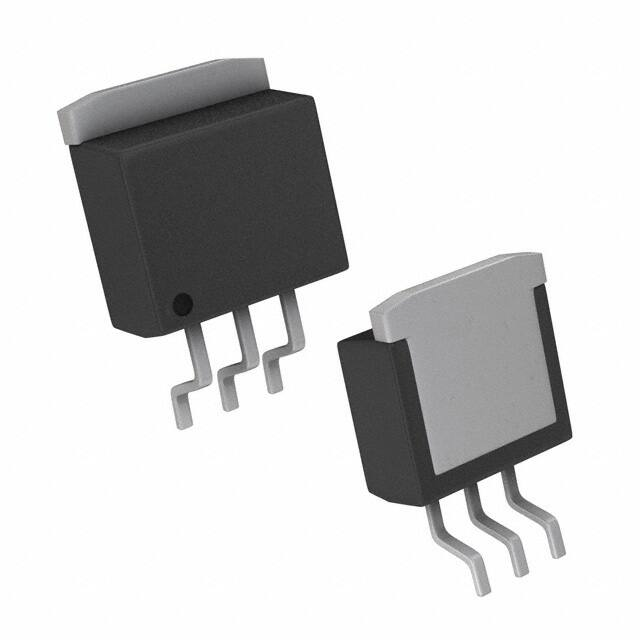
DT PACKAGE (D-Pak)
(Top View)
* Pin 1 is GND for fixed voltage versions.
BLOCK DIAGRAM
VIN
Bias
Circuit
Thermal
Limit Circuit
Bandgap
Circuit
Control
Circuit
Output
Circuit
VOUT
SOA Protection
Circuit
ADJ or
GND*
Current
Limit Circuit
* This pin GND for fixed voltage versions.
2
Copyright © 1999
Rev. 1.7a 10/00
�PRODUCT DATABOOK 1996/1997
LX8386-xx/8386A-xx/8386B-xx
1 . 5 A LOW DR O P O U T P OSITIVE R E G U L AT O R S
P
R O D U C T I O N
D
A T A
S
H E E T
ELECTRICAL CHARACTERISTICS
(Unless otherwise specified, these specifications apply over the operating ambient temperatures for the LX8386/86A/86B-xxC with 0°C ≤ TA ≤ 125°C,
and the LX8386-xxI with -25°C ≤ TA ≤ 125°C; VIN - VOUT = 3V; IOUT = 1.5A. Low duty cycle pulse testing techniques are used which maintains junction
and case temperatures equal to the ambient temperature.)
LX8386/86A/86B-00 (Adjustable)
Parameter
Reference Voltage
(Note 4)
LX8386/86A-00
Symbol
Test Conditions
VREF
IOUT = 10mA, TA = 25°C
10mA ≤ IOUT ≤ IOUT (MAX), 1.5V ≤ (VIN - VOUT), VIN ≤ 10V, P ≤ PMAX
LX8386B-00
IOUT = 10mA, TA = 25°C
10mA ≤ IOUT ≤ IOUT (MAX), 1.5V ≤ (VIN - VOUT), VIN ≤ 10V, P ≤ PMAX
Line Regulation (Note 2)
∆VREF(VIN ) 1.5V ≤ (VIN - V OUT) ≤ 7V, IOUT = 10mA
Load Regulation (Note 2)
∆VREF(IOUT) VIN - V OUT = 3V, 10mA ≤ IOUT ≤ 1.5A
Thermal Regulation
∆VOUT (Pwr) TA = 25°C, 20ms pulse
Ripple Rejection (Note 3)
VOUT = 5V, f =120Hz, COUT = 100µf Tantalum, VIN = 6.5V
CADJ = 10µF, I OUT = 1.5A
Adjust Pin Current
I ADJ
Adjust Pin Current Change (Note 4)
∆IADJ
10mA ≤ IOUT ≤ IOUT (MAX) , 1.5V ≤ (VIN - VOUT), VIN ≤ 10V
Dropout Voltage
LX8386-00
∆V
∆VREF = 1%, IOUT = 1.5A
LX8386A/86B-00
∆VREF = 1%, IOUT = 1.5A
Minimum Load Current
IOUT (MIN) VIN ≤ 10V
Maximum Output Current
IOUT (MAX) (VIN - VOUT) ≤ 7V
Temperature Stability (Note 3)
∆VOUT (T)
Long Term Stability (Note 3)
∆VOUT (t) TA = 125°C, 1000 hours
RMS Output Noise (% of VOUT) (Note 3) VOUT (RMS) TA = 25°C, 10Hz ≤ f ≤ 10kHz
LX8386/86A/86B-00
Min. Typ.
Max.
1.238
1.225
1.240
1.238
65
1.5
Units
1.250
1.250
1.250
1.250
0.015
0.15
0.01
83
1.262
1.270
1.260
1.262
0.2
0.4
0.04
V
V
V
V
%
%
%/W
dB
55
0.2
1.2
1.1
2
2.0
0.25
0.3
0.003
100
5
1.5
1.3
10
µA
µA
V
V
mA
A
%
%
%
1
LX8386/86A/86B-33 (3.3V Fixed)
Parameter
Output Voltage
(Note 4)
LX8386-33
Symbol
VOUT
Test Conditions
VIN = 5V, IOUT = 0mA, TA = 25°C
4.75V ≤ V IN ≤ 10V, 0mA ≤ IOUT ≤ 1.5A, P ≤ PMAX
LX8386A/86B-33
VIN = 5V, IOUT = 0mA, TA = 25°C
4.75V ≤ V IN ≤ 10V, 0mA ≤ IOUT ≤ 1.5A, P ≤ PMAX
Line Regulation (Note 2)
∆VOUT 4.75V ≤ V IN ≤ 7V
(VIN )
4.75V ≤ VIN ≤ 10V
Load Regulation (Note 2)
∆VOUT (IOUT) VIN = 5V, 0mA ≤ IOUT ≤ IOUT (MAX)
Thermal Regulation
∆VOUT (Pwr) TA = 25°C, 20ms pulse
Ripple Rejection (Note 3)
COUT = 100µF (Tantalum), IOUT = 1.5A
Quiescent Current
IQ
0mA ≤ IOUT ≤ IOUT (MAX) , 4.75V ≤ VIN ≤ 10V
Dropout Voltage
LX8386-33
∆V
∆VOUT = 1%, IOUT ≤ IOUT (MAX)
LX8386A/86B-33
∆VOUT = 1%, IOUT ≤ IOUT (MAX)
Maximum Output Current
IOUT (MAX) VIN ≤ 7V
Temperature Stability (Note 3)
∆VOUT (T)
Long Term Stability (Note 3)
∆VOUT (t) TA = 125°C, 1000 hours
RMS Output Noise (% of VOUT) (Note 3) VOUT (RMS) TA = 25°C, 10Hz ≤ f ≤ 10kHz
LX8386/86A/86B-33
Min. Typ.
Max.
3.267
3.235
3.274
3.267
60
1.5
3.30
3.30
3.30
3.30
1
2
5
0.01
83
4
1.2
1.1
2.0
0.25
0.3
0.003
3.333
3.365
3.326
3.333
6
10
15
0.02
10
1.5
1.3
1
Units
V
V
V
V
mV
mV
mV
%/W
dB
mA
V
V
A
%
%
%
Note 2. Regulation is measured at constant junction temperature, using pulse testing with a low duty cycle. Changes in output voltage due to
heating effects are covered under the specification for thermal regulation.
Note 3. These parameters, although guaranteed, are not tested in production.
Note 4. See Maximum Output Current Section above.
Copyright © 1999
Rev. 1.7a 10/00
3
�PRODUCT DATABOOK 1996/1997
LX8386-xx/8386A-xx/8386B-xx
1 . 5 A LOW D R O P O U T P OSITIVE R E G U L AT O R S
P
R O D U C T I O N
D
A T A
S
H E E T
A P P L I C AT I O N N O T E S
The LX8386/86A/86B series ICs are easy to use Low-Dropout (LDO)
voltage regulators. They have all of the standard self-protection
features expected of voltage regulators: short circuit protection, safe
operating area protection and automatic thermal shutdown if the
device temperature rises above approximately 165°C.
Use of an output capacitor is REQUIRED with the LX8386/86A/
86B series. Please see the table below for recommended minimum
capacitor values.
These regulators offer a more tightly controlled reference voltage
tolerance and superior reference stability when measured against
the older pin-compatible regulator types that they replace.
STABILITY
The output capacitor is part of the regulator’s frequency compensation system. Many types of capacitors are available, with different
capacitance value tolerances, capacitance temperature coefficients,
and equivalent series impedances. For all operating conditions,
connection of a 220µF aluminum electrolytic capacitor or a 47µF
solid tantalum capacitor between the output terminal and ground
will guarantee stable operation.
If a bypass capacitor is connected between the output voltage
adjust (ADJ) pin and ground, ripple rejection will be improved
(please see the section entitled “RIPPLE REJECTION”). When ADJ
pin bypassing is used, the required output capacitor value increases.
Output capacitor values of 220µF (aluminum) or 47µF (tantalum)
provide for all cases of bypassing the ADJ pin. If an ADJ pin bypass
capacitor is not used, smaller output capacitor values are adequate.
The table below shows recommended minimum capacitance values
for stable operation.
RECOMMENDED CAPACITOR VALUES
INPUT
OUTPUT
ADJ
10µF
10µF
15µF Tantalum, 100µF Aluminum
47µF Tantalum, 220µF Aluminum
None
15µF
In order to ensure good transient response from the power supply
system under rapidly changing current load conditions, designers
generally use several output capacitors connected in parallel. Such
an arrangement serves to minimize the effects of the parasitic
resistance (ESR) and inductance (ESL) that are present in all
capacitors. Cost-effective solutions that sufficiently limit ESR and
ESL effects generally result in total capacitance values in the range
of hundreds to thousands of microfarads, which is more than
adequate to meet regulator output capacitor specifications. Output
capacitance values may be increased without limit.
The circuit shown in Figure 1 can be used to observe the transient
response characteristics of the regulator in a power system under
changing loads. The effects of different capacitor types and values
on transient response parameters, such as overshoot and undershoot, can be quickly compared in order to develop an optimum
solution.
4
Power Supply
IN
LX8386
/8386A/8386B
OUT
ADJ
Minumum Load
(Larger resistor)
Full Load
(Smaller resistor)
RDSON


 工商网监
湘ICP备2023018690号
工商网监
湘ICP备2023018690号
