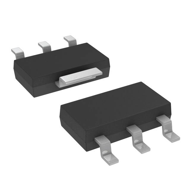
LX8415-33CST

LX8415-33CST

  • 厂商:

    MICROSEMI(美高森美)

  • 封装:

    TO-261-4

  • 描述:

    IC REG LIN 3.3V 500MA SOT223 PWR

  • 详情介绍
  • 数据手册
  • 价格&库存
LX8415-33CST 数据手册
LIN D O C # : 8415 LX8415-xx 0 . 5 A L O W D ROPOUT P OSITIVE REGULATORS T HE I NFINITE P OWER OF I N N O VAT I O N P RELIMINARY D ATA S HEET DESCRIPTION The LX8415 series ICs are positive Low Dropout (LDO) regulators. At the designed maximum load current, the LX8415 series dropout voltage is guaranteed to be 1.3V or lower at 0.5A. The dropout voltage decreases with load current. The LX8415 is available in an adjustable output voltage version and fixed output versions of 2.5V and 3.3V. Onchip trimming of the internal voltage reference allows specification of the initial output voltage to within ±1% of its nominal value. The output currentlimit point is also trimmed, which helps to minimize stress on both the regulator and the system power source when they are operated under short-circuit conditions. The regulator's internal circuitry will operate at input-to-output differential voltages down to 1V. Most regulator circuit designs include output capacitors with values in the range of tens to hundreds of microfarads or more. The LX8415 typically requires at least 10µF of output capacitance for stable operation. The LX8415 is available in the lowprofile plastic SOT-223 package for applications where space is at a premium. K E Y F E AT U R E S s 0.7% Line Regulation Maximum s 0.7% Load Regulation Maximum s Output Current Of 500mA s Regulates To 40ºC/W depending on mounting technique. (See Application Notes Section: Thermal Considerations) BLOCK D IA GR A M VIN Bias Circuit Thermal Limit Circuit Bandgap Circuit Control Circuit Output Circuit VOUT ADJ Current Limit Circuit 2 Copyright © 1999 Rev. 0.4 1/99 PRODUCT DATABOOK 1996/1997 LX8415-xx 0 . 5 A L O W D ROPOUT P OSITIVE REGULATORS P RELIMINARY D ATA S HEET R E C O M M E N D E D O P E R AT I N G C O N D I T I O N S Parameter Input Voltage Operating Voltage LX8415-xx Operating Ambient Temperature Range Note 2. Range over which the device is functional. (Note 2) Symbol Recommended Operating Conditions Min. Typ. Max. 7 125 Units 0 V °C ELECTRICAL CHARACTERISTICS (Unless otherwise specified: 0°C ≤ TJ ≤ 125°C, IMAX = 0.5A for the LX8415-xx.) Parameter Reference Voltage Output Voltage LX8415-00 LX8415-25 LX8415-33 Line Regulation (Note 3) Load Regulation (Note 3) Dropout Voltage (Note 4) LX8415-00 LX8415-25 / 33 LX8415-00 LX8415-25 / 33 LX8415-xx Symbol VREF Test Conditions IOUT = 10mA, (VIN - VOUT) = 2V, TJ = 25°C 10mA ≤ IOUT ≤ IMAX, 1.5V ≤ (VIN - VOUT) ≤ 6V IOUT = 10mA, VIN = 5V, TJ = 25°C 0mA ≤ IOUT ≤ IMAX, 4.75V ≤ V IN ≤ 6V IOUT = 10mA, VIN = 5V, TJ = 25°C 0mA ≤ IOUT ≤ IMAX, 4.75V ≤ V IN ≤ 6V I OUT = 10mA, 1.5V ≤ VIN - V OUT ≤ 6V I OUT = 0mA, 4.75V ≤ V IN ≤ 6V (V IN - VOUT) = 3V, 10mA ≤ IOUT ≤ IMAX VIN = 4.75V, 0mA ≤ IOUT ≤ IMAX IOUT = 100mA IOUT = 300mA IOUT = IMAX (V IN - VOUT) ≥ 1.3V, T J = 25°C VIN ≤ 6V, (LX8415-00) VIN ≤ 6V TA = 25°C, 30ms Pulse fRIPPLE = 120Hz, (VIN - VOUT ) = 3V, VRIPPLE = 1Vp - p Min. 1.238 1.225 2.475 2.450 3.267 3.235 LX8415-xx Typ. Max. 1.250 1.250 2.500 2.500 3.300 3.300 0.05 1 0.15 10 1.05 1.10 1.15 950 0.5 4.5 0.08 75 60 0.2 0.5 0.3 0.003 1.262 1.275 2.525 2.550 3.333 3.365 0.7 7 0.5 20 1.20 1.25 1.30 10 10 0.2 130 5 Units V V V V V V % mV % mV V V V mA mA mA %/W dB µA µA % % % Current Limit LX8415-xx I OUT (MAX) Minimum Load Current (Note 5) Quiescent Current LX8415-25 / 33 Thermal Regulation Ripple Rejection Adjust Pin Current LX8415(A)-00 Adjust Pin Current Change LX8415(A)-00 10mA ≤ IOUT ≤ IMAX, 1.5V ≤ (VIN - VOUT) ≤ 6V Temperature Stability Long Term Stability TA = 125°C, 1000Hrs RMS Output Noise (% of V OUT), 10Hz ≤ f ≤ 10kHz 500 60 Notes: 3. See thermal regulation specification for changes in output voltage due to heating effects. Load regulation and line regulation are measured at a constant junction temperature by low duty cycle pulse testing. 4. Dropout voltage is specified over the full output current range of the device. Dropout voltage is defined as the minimum input/output differential measured at the specified output current. Test points and limits are also shown on the Dropout Voltage Curve. 5. Minimum load current is defined as the minimum output current required to maintain regulation. Copyright © 1999 Rev. 0.4 1/99 3 PRODUCT DATABOOK 1996/1997 LX8415-xx 0 . 5 A L O W D ROPOUT P OSITIVE R EGULATORS P RELIMINARY D ATA S HEET A P P L I C AT I O N N O T E S The LX8415 series ICs are easy to use Low-Dropout (LDO) voltage regulators. They have the standard self-protection features expected of a voltage regulator: short circuit protection and automatic thermal shutdown if the device temperature rises above approximately 165°C. Use of an output capacitor is REQUIRED with the LX8415 series. Please see the table below for recommended minimum capacitor values. These regulators offer a more tightly controlled reference voltage tolerance and superior reference stability when measured against the older pin-compatible regulator types that they replace. STABILITY The output capacitor is part of the regulator’s frequency compensation system. Many types of capacitors are available, with different capacitance value tolerances, capacitance temperature coefficients, and equivalent series impedances. For all operating conditions, connection of a 220µF aluminum electrolytic capacitor or a 47µF solid tantalum capacitor between the output terminal and ground will guarantee stable operation. If a bypass capacitor is connected between the output voltage adjust (ADJ) pin and ground, ripple rejection will be improved (please see the section entitled “RIPPLE REJECTION”). When ADJ pin bypassing is used, the required output capacitor value increases. Output capacitor values of 220µF (aluminum) or 47µF (tantalum) provide for all cases of bypassing the ADJ pin. If an ADJ pin bypass capacitor is not used, smaller output capacitor values are adequate. The table below shows recommended minimum capacitance values for stable operation. RECOMMENDED CAPACITOR VALUES INPUT 10µF 10µF Power Supply IN LX8415-xx ADJ OUT Minumum Load (Larger resistor) Full Load (Smaller resistor) C1 C2 RDSON
LX8415-33CST
物料型号: - LX8415系列IC有可调输出电压版本和固定输出版本,包括2.5V和3.3V两种固定输出电压,以及可调输出电压版本(LX8415-00)。

器件简介: - LX8415系列是一款正压低dropout(LDO)稳压器。在设计的最大负载电流下,LX8415系列的dropout电压保证在1.3V或更低(0.5A负载时)。随着负载电流的减少,dropout电压也随之降低。

引脚分配: - LX8415采用SOT-223表面贴装封装,具有3个引脚:输入引脚、输出引脚和调整引脚(ADJ)。

参数特性: - 线规:最大0.7% - 负载规:最大0.7% - 输出电流:最大500mA - dropout电压:低于1.3V - 内部电压参考精度:±1%

功能详解: - LX8415系列IC具有短路保护和热关断保护功能,以防设备温度超过大约165°C。 - 需要使用输出电容器,推荐至少10pF的输出电容以保证稳定工作。

应用信息: - 电池充电器、5V转3.3V线性稳压器、开关电源后的稳压器、调制解调器、DVD播放器等。

封装信息: - LX8415系列IC采用SOT-223低轮廓塑料封装,适用于空间受限的应用。所有表面贴装封装均可提供卷带封装。

LX8415-33CST 价格&库存

很抱歉,暂时无法提供与“LX8415-33CST”相匹配的价格&库存,您可以联系我们找货

免费人工找货