P
ATENTS
TM
P
ENDING
RangeMAX
T
HE
LXM1621-xx
D
ATA
D IGITAL D IMMING D UAL L AMP C CFL I NVERTER M ODULE
I
NFINITE
P
OWER
OF
I
NNOVATION
P
RELIMINARY
S
HEET
DESCRIPTION RangeMAX Wide Range Dimming, Dual Output Inverter. The LXM1621 Direct DriveTM CCFL (Cold Cathode Fluorescent Lamp) Inverter Modules are specifically designed for driving LCD backlight lamps. Similar to the LXM1620, the LXM1621 excels in applications where critical parameters include very wide range dimmability, high efficiency and reliable fail-safe design in a small form factor. These 12 volt input modules are specifically designed with desktop and industrial applications in mind. Unlike the LXM1620 or any traditional dimming CCFL inverters, the LXM1621 provides the designer a vastly superior display brightness range. 1000:1+ brightness range is achievable with a standard LCD display (see Product Highlight). Our wide range dimming provides exceptional display readability at less than 1% of full brightness, allowing both power savings and low ambient light operating capability (i.e. "night readable"). RangeMAX Digital Dimming Technique. Digital dimming provides flicker-free brightness control in any wide-range dimming application. Dimming ratios as great as 1000:1 can be achieved. Incorporation of a video synchronization feature allows wide ratio dimming without the display disturbances and interference seen with competitive products. The modules are equipped with a dimming input that permits brightness control from an external potentiometer or DC voltage source. The resultant "burst drive" that energizes the lamp was designed specifically to ensure that no premature lamp degradation occurs (see "How RangeMAX Works" Section). Fail-safe Feature For Multiple Lamp Applications. Our multi-output inverters are designed to keep your application operating at near normal brightness in the event that a lamp fails. This allows the display to remain "on-line" until lamp replacement is convenient. Direct Drive Technology. The module design is based on a new Direct Drive topology, which provides a number of cost and performance advantages. The LXM1621-xx Direct Drive inverters eliminate the classic resonant inductor and capacitors, thus reducing cost and allowing a substantial reduction in module size. Universal Connector Configuration. Linfinity's multiple lamp inverters include a built in connector array for the most common LCD lamp configurations. Additional Features. Other benefits of this new topology are fixed-frequency operation and secondary-side strike-voltage regulation. Strike-voltage regulation minimizes corona discharge in the output transformer and related circuitry, providing longer life and higher reliability. All LXM1621 modules feature both open and shorted lamp protection. The LXM1621 is fully customizable (electronically and mechanically) to specific customer requirements.
I I I I I I
K E Y F E AT U R E S
RangeMAX Wide Range Dimming 8V To 18V Input Voltage Range Small Form Factor Easy To Use Brightness Control MicroAmp SLEEP Mode Output Short-Circuit Protection And Automatic Strike-Voltage Regulation I Fixed Frequency Operation I Universal Connector Configuration
A P P L I C AT I O N S
I Hi-Brite Displays I Desktop Displays I Low Ambient Light Conditions (i.e. Aircraft Cabins, Automobile) I Industrial Applications
BENEFITS
I High Efficiency Reduces Heating Problems I Smooth, Flicker Free 0-100% Full-Range Brightness Control Gives Your Product A High Quality Image I Output Open Circuit Voltage Regulation Minimizes Corona Discharge For Long Life And High Reliability I Power Efficient, "Low Brightness" Capability Allows For Advanced Power Management
NOTE: For current data & package dimensions, visit our web site: http://www.linfinity.com.
M O D U L E O R D E R I N F O R M AT I O N Part Number Lamp Run Voltage Lamp Current
LXM1621-01 LXM1621-02 LXM1621-03
500 - 750VRMS 350 - 500VRMS 350 - 500VRMS
7mA 6mA 6.5mA
Copyright © 2000 Rev. 0.6 2/00
LINFINITY MICROELECTRONICS INC.
11861 WESTERN AVENUE, GARDEN GROVE, CA. 92841, 714-898-8121, FAX: 714-893-2570
1
�PATENT PENDING
PRODUCT DATABOOK 1996/1997
LXM1621-xx
D IGITAL D IMMING D UAL L AMP C CFL I NVERTER M ODULE
P
RELIMINARY
RangeMAX
D
ATA
TM
S
HEET
(Note 1)
A B S O L U T E M A X I M U M R AT I N G S
Input Supply Voltage (VIN) ........................................................................................................................................................ -0.3V to 18V Output Voltage, no load .............................................................................................................................. Internally Limited to 1800VRMS Output Current ............................................................................................................................................. 10.0mARMS (Internally Limited) Output Power (per Lamp) .................................................................................................................................................................... 6.0W Input Signal Voltage (BRITE Input) ....................................................................................................................................... -0.3V to 6.5V Input Signal Voltage (SLEEP, VSYNC Inputs) ................................................................................................................................... -0.3V to VIN Ambient Operating Temperature .................................................................................................................................................... 0°C to 70°C Storage Temperature Range ......................................................................................................................................................... -40°C to 85°C
Note 1. Exceeding these ratings could cause damage to the device. All voltages are with respect to Ground. Currents are positive into, negative out of the specified terminal.
R E C O M M E N D E D O P E R A T I N G C O N D I T I O N S (R.C.) This module has been designed to operate over a wide range of input and output conditions. However, best efficiency and performance will be obtained if the module is operated under the condition listed in the 'R.C.' column. Min. and Max. columns indicate values beyond which the inverter, although operational, will not function optimally. Parameter
Input Supply Voltage Range (Functional) Input Supply Voltage (Fully Regulated Lamp Current) Output Power (per Lamp) LXM1621-01 LXM1621-02/-03 Brightness Control Input Voltage Range Lamp Operating Voltage LXM1621-01 LXM1621-02/-03 Lamp Current (Full Brightness - per Lamp) LXM1621-01 LXM1621-02 LXM1621-03 Operating Ambient Temperature Range
Symbol
VIN PO VBRT ADJ V LAMP IOLAMP
Recommended Operating Conditions Min. R.C. Max.
8 10.2 12 12 4 2.5 625 425 7.0 6.0 6.5 18 13.8 5 3 2.5 750 500
Units
V V W W V V RMS V RMS mARMS mARMS mARMS °C
0.0 500 350
TA
0
70
ELECTRICAL CHARACTERISTICS
Unless otherwise specified, these specifications apply over the recommended operating conditions and 25°C ambient temperature for the LXM1621-xx.
Parameter Output Pin Characteristics
1621-01 1621-02 1621-03 Minimum Lamp Current (per Lamp) (Notes 2 & 3) Lamp Start Voltage Operating Frequency Full Bright Lamp Current
(per Lamp)
Symbol
Test Conditions
LXM1621-xx Min. Typ. Max.
6.3 5.5 5.7 7.0 6.0 6.5 0.14 0.035 57 -8 2.5 0 -50 7.7 6.5 7.1
Units
IL (MAX)
IL (MIN) VLS fO IBRT VC VC
VBRT ADJ = 2.5VDC, SLEEP = HIGH, Burst Duty = 100%, VIN = 12VDC VBRT ADJ = 2.5VDC, SLEEP = HIGH, Burst Duty = 100%, VIN = 12VDC VBRT ADJ = 2.5VDC, SLEEP = HIGH, Burst Duty = 100%, VIN = 12VDC VBRT ADJ = 0VDC, SLEEP = HIGH, Burst Duty = 2%, VIN = 9VDC VBRT ADJ = -50mVDC, SLEEP = HIGH, Burst Duty = 0.5%, VIN = 9V DC 0°C < TA < 40°C, VIN ≥ 10.8VDC VBRT ADJ = 2.5VDC, SLEEP = HIGH, VIN = 12VDC VBRT ADJ = 0VDC IO (LAMP) = 100% Duty Cycle IO (LAMP) = 2% Duty Cycle IO (LAMP) = 0.5% Duty Cycle
1500 52 -6
1800 62 -10 2.6 0
mARMS mARMS mARMS mARMS mARMS V RMS KHz µADC VDC VDC mVDC VDC VDC µADC
BRITE Input
Input Current Input Voltage for Max. Lamp Current Input Voltage for Min. Lamp Current (Note 3)
SLEEP Input
RUN Mode SLEEP Mode Input Current VSLEEP (HI) VSLEEP (LO) ISLEEP 2.2 -0.3 70 VIN 0.8 100
SLEEP = 5.0V
75
Note 2. Minimum lamp current required to maintain even light output may vary with display panel. 3. See 1000:1 Dimming Application section for details.
2
Copyright © 2000 Rev. 0.6 2/00
�PRODUCT DATABOOK 1996/1997
PATENT PENDING
RangeMAX
TM
LXM1621-xx
D IGITAL D IMMING D UAL L AMP C CFL I NVERTER M ODULE
P
RELIMINARY
D
ATA
S
HEET
( Continued)
ELECTRICAL CHARACTERISTICS Parameter VSYNC Characteristics
Logic High Level Logic Low Level Input Impedance Pulse Width (Note 4) Input Frequency VSYNC (HI) V SYNC (LO) ZIN tPW fSYNC IIN (MIN) V IN = 12VDC , SLEEP ≤ 0.8V
Symbol
Test Conditions
LXM1621-xx Min. Typ. Max.
4.0 -0.3 60 25 49 6.5 1.0 75 250 150 50
Units
66
VDC VDC kΩ µs Hz µADC
Power Characteristics
Sleep Current 5 Note 4. The module will be functional with pulse widths much larger than 250µs.
FUNCTIONAL PIN DESCRIPTION
Conn. CN1
CN1-1 CN1-2 CN1-3 CN1-4 CN1-5 CN1-6 CN1-7, 8
Pin
Description
VIN GND SLEEP BRITE VSYNC
Input Power Supply. (8V ≤ VIN ≤ 18V) Power Supply Return. ON/OFF Control. (2.2V < SLEEP < VIN = ON, -0.3V < SLEEP < 0.8V = OFF) Brightness Control (-0.3V to 2.5VDC). 2.5VDC gives maximum lamp current. Vertical syncronization input. 49Hz < fSYNC < 150Hz
CN2 thru CN5: Refer to Figure 2
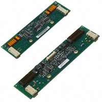
PHYSICAL DIMENSIONS
LXM1621-xx
All dimensions are in inches (mm)
4.88 (124)
CN2
(Bottom Side)
CN3
(Bottom Side)
CN1
0.24 (6)
CN4
1.50 (38)
1.89 (48)
Ø 0.12 (3.0)
Grounded Mounting Hole - 2 plcs Warning!! High Voltage Present At All Output Connectors
0.338 (8.6) Max.
0.060 (1.52) max.
Copyright © 2000 Rev. 0.6 2/00
CN5
1.26 (32)
3
�PATENT PENDING
PRODUCT DATABOOK 1996/1997
LXM1621-xx
D IGITAL D IMMING D UAL L AMP C CFL I NVERTER M ODULE
P
RELIMINARY
RangeMAX
D
ATA
TM
S
HEET
T Y P I C A L C O N N E C T I O N C O N F I G U R AT I O N S
CCFL Lamps
CN5
CN5
LXM1621-xx
LXM1621-xx
CN1
CN1
CCFL Lamps
CN4
CN4
Desktop Display
Desktop Display
CN5
CN3
LXM1621-xx
CN4
CN2
CCFL Lamps
CCFL Lamps
Desktop Display
Desktop Display
* Connectors CN2 and CN3 are on the bottom side of the inverter. View shown is looking through the board.
FIGURE 1 — Connectivity Configuration Examples These examples illustrate four typical LCD wiring configurations that are accomodated by Linfinity's unique connector array. Linfinity inverters have multiple lamp connector styles that are common to the industry, which are duplicated at both ends of the module. This permits over 12 variations of module mounting and interconnectivity configurations.
4
Copyright © 2000 Rev. 0.6 2/00
LXM1621-xx*
CN1
CN1
�PRODUCT DATABOOK 1996/1997
PATENT PENDING
RangeMAX
TM
LXM1621-xx
D IGITAL D IMMING D UAL L AMP C CFL I NVERTER M ODULE
P
RELIMINARY
D
ATA
S
HEET
C O N N E C T O R S C H E M AT I C
CN1
8 4 3 2 1 N.C. 1 2 3 1 1 2
VHI1
VHI2
3 2 1
N.C.
3 4
Inverter Output 1
CN2
Inverter Output 2
CN3
CN4
CN5
FIGURE 2 — LXM1621-xx Connector Schematic Note: CN2 and CN3 (shown with dashed lines) are located on the opposite side of the PCB from CN1, CN4 and CN5. Their pin numbers are shown as viewed looking through the printed circuit board.
Connectors: CN1 = MOLEX 53261-0890 CN2, CN3 = JST SM04(4.0)B-BHS-1-TB CN4, CN5 = JST SM03(4.0)B-BHS-1-TB
Connection Rules
Mates With: Pins: 50079-8100*, Housing: 51021-0800
* Loose (-8000, Chain) Recommended #26 AWG wiring
JST BHR-04VS-1 JST BHR-03VS-1
1. Always install two (2) lamps. Operating with only one lamp may overdrive lamp current at maximum brightness settings. 2. Verify lamp wiring before connecting lamps to the inverter module. Connecting both lamps to one of the two inverter output circuits will result in reduced brightness. The LXM1621-xx module connectors are wired per industry standard. The lamphot wires (high voltage wires) are always on pin 1 or 2, and thecold wire (low voltage wire) is always on pin 3 or 4. F A I L S A F E F E AT U R E F O R M U L T I P L E L A M P O P E R A T I O N S Our multi-output inverters are designed to keep your application operating at near normal brightness in the event that a lamp fails. This allows the display to remain "on-line" until lamp replacement is convenient. Linfinity "pairs" the lamps so that if one lamp in the pair breaks, most of its current is added to the good lamp. CCFLs will respond with more brightness for a period of time. Operating time in this mode will be a function of the lamps age but should be typically in the order of hundreds of hours. This operating characteristic can provide adequate display performance for a limited, but useful period of time. Shortening of the lamp life in this mode is typically not a concern as it is recommended that all lamps in a display be replaced at the same time.
Lamps
IS
FIGURE 3 — Dual Output Stage
Copyright © 2000 Rev. 0.6 2/00
5
�PATENT PENDING
PRODUCT DATABOOK 1996/1997
LXM1621-xx
D IGITAL D IMMING D UAL L AMP C CFL I NVERTER M ODULE
P
RELIMINARY
RangeMAX
D
ATA
TM
S
HEET
HOW RANGEMAX WORKS
LAMP VOLTAGE & LAMP CURRENT — Burst Mode Operation
(770VRMS)
(760VRMS)
(7.6mARMS)
(6.7mARMS)
FIGURE 4 — 50% Burst Duty Cycle
FIGURE 5 — 2% Burst Duty Cycle
Rather than using the traditional dimming technique of varying lamp current magnitude to adjust light output, RangeMAX inverters use a fixed lamp current value with a duty cycle control method. The lamp current burst width can be modulated from 100% (continuous lamp current) down to a 2% duty cycle, allowing the lamp to be dimmed to less than 1% of its full brightness. As can be seen in Trace 4 of Figure 6, careful design consideration was given to controlling lamp start voltage to softly start current flow. This eliminates current overshoot that can result in premature cathode wear and reduce lamp life.
(760VRMS)
(6.7mARMS)
FIGURE 6 — 2% Burst Duty Cycle (Expanded Time Base)
VBRITE 0-2.5V DC Ramp
Comparator Transformer Driver
High Voltage Transformer
VHI1
Ramp Gen. VSYNC ISENSE
VSENSE
VLO
FIGURE 7 — RangeMAX Block Diagram
LAMP 1
6
Copyright © 2000 Rev. 0.6 2/00
�PRODUCT DATABOOK 1996/1997
PATENT PENDING
RangeMAX
TM
LXM1621-xx
D IGITAL D IMMING D UAL L AMP C CFL I NVERTER M ODULE
P
RELIMINARY
D
ATA
S
HEET
H O W R A N G E M A X W O R K S (continued)
HIGHLIGHTS
I On-board brightness control circuit includes a DC voltage to pulse width converter that minimizes system design work and system noise susceptibility. This provides a familiar and convenient interface while reducing the potential for externally induced noise which can cause lamp flicker. I An on-board oscillator operates the inverter BURST rate above 95Hz, well beyond standard 50/60Hz video refresh rates where the eye can perceive pulsing light. I RangeMAX inverter modules are designed to operate with the burst frequency synchronized to the video frame rate. This provides operation with no visible display disturbances caused by beat frequencies between the lamps and video frame rates. I In applications with no access to a vertical sync, the inverter burst frequency can be allowed to "free run" at 95Hz. In this non-synchronous mode, minor display disturbances may be found under certain video conditions. This performance is acceptable for many applications, but synchronization must be used when no disturbance can be tolerated. I Separate feedback loops for lamp current and open circuit voltage regulation insure reliable strike under all operating conditions, automatic over-voltage prevention with broken or failed lamps, and accurate lamp current regulation.
T Y P I C A L 1 0 0 : 1 D I M M I N G A P P L I C AT I O N
2.5VDC
8VDC- 18VDC
£ 10k
BRITE
VIN
VHI2 VHI1
Lamp 1 Lamp 2
LXM1621-xx
0V 5V SLEEP VSYNC VSYNC
FIGURE 8 — Potentiometer Brightness Control
GND
VLO
I The brightness control may be a simple 10k potentiometer or a voltage output DAC. A PWM signal from a micro-controller may also be used with a suitable filter such as shown in Figure 8A. I If synchronization to the video framerate is desired, connect the vertical sync pulse from the system video controller to the appropriate VSYNC input. If no video synchronization is desired, connect VSYNC to ground. I If you need to turn the inverter ON/OFF remotely, connect a 3V or 5V logic signal to the SLEEP input. If remote ON/ OFF is not needed, connect the SLEEP input to VIN or any other voltage greater than 2.2VDC. I Connect VHI t o high voltage wire from the lamp. Connect VLO to the low voltage wire (wire with thinner insulation). If both lamp wires have heavy high voltage insulation, connect the longest wire to VLO. VLO is connected directly to ground (GND pin) on the inverter PCB. Always insure a good lamp return by using a wire. Do not rely on a chassis ground connection.
PWM Signal from System
P.W. £ 100µs
4.99k 4.7µF 4.99k* BRITE
LXM1621-xx
0 £ P.W. £ 100% of period
* use 4.99k for 5V PWM amplitude, 15k for 3.3V PWM amplitude, and omit for 2.5V PWM amplitude.
FIGURE 8A — PWM Brightness Control
Copyright © 2000 Rev. 0.6 2/00
7
�PATENT PENDING
PRODUCT DATABOOK 1996/1997
LXM1621-xx
D IGITAL D IMMING D UAL L AMP C CFL I NVERTER M ODULE
P
RELIMINARY
RangeMAX
D
ATA
TM
S
HEET
1 0 0 0 : 1 D I M M I N G A P P L I C AT I O N The following application defines techniques capable of delivering dimming ranges in the 250:1 and 1000:1 range. As is widely understood, these techniques will provide general capabilities and actual system performance will vary with panel design, CCFTs, ambient temperature and a number of other variables outside the control of the inverter. These methods can be used in conjunction with other techniques such as lamp heating and matching.
7
IOLAMP (mA)
0.7 .14
Wide ratio (1000:1) dimming can be accomplished using the Linfinity inverter in two ways: 1) By varying the input voltage on the brightness pin as indicated in Figure 9. Caution must be exercised when applying negative voltage to the brightness control input. Applying more than -300mV to any inverter input will cause inverter malfunction (see Absolute Maximum Ratings). 2) By making a resistor value change on the module. If this option is preferrable, please contact the factory for application assistance. Both methods discussed will provide a lower duty cycle operation than is necessary in a 100:1 dimming application. Careful consideration should be made with regards to display quality at these dimming levels. At very low brightness levels, even very small amounts of noise on the VBRITE line can cause flicker on the display, so special care must be given to grounding, filtering and shielding the inverter from the digital logic and clock.
.070 -100mV 0V 2.5V
VBRT ADJ (V) FIGURE 9 — Average Lamp Current vs. VBRITE Voltage (per Lamp)
RangeMAX INVERTERS
Also available in Single Output LXM1611-01, LXM1612-xx or Quad Output LXM1641-01 versions for multiple lamp applications.
RangeMAX and Direct Drive are trademarks of Linfinity Microelectronics Inc.
PRELIMINARY DATA - Information contained in this document is pre-production data, and is proprietary to LinFinity. It may not modified in any way without the express written consent of LinFinity. Product referred to herein is offered in sample form only, and Linfinity reserves the right to change or discontinue this proposed product at any time.
8
Copyright © 2000 Rev. 0.6 2/00
�