ULTRA LOW NOISE, MEDIUM CURRENT
D-PHEMT Transistor
50Ω
SAV-331+
10-4000 MHz
THE BIG DEAL
y Low Noise Figure, 0.5 dB typ. at 300 MHz
y Gain, 24.1 dB typ. at 300 MHz
y High Output IP3, +32.3 dBm typ. at 300 MHz
y Output Power at 1dB comp., +19.6 dBm typ. at 300 MHz
y Low Current, 60mA
y External biasing and matching required
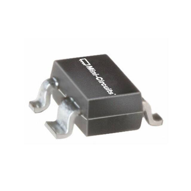
Generic photo used for illustration purposes only
CASE STYLE: MMM1362
+RoHS Compliant
The +Suffix identifies RoHS Compliance. See our web site
for RoHS Compliance methodologies and qualifications
APPLICATIONS
y Cellular
y ISM
y GSM
y WCDMA
y WiMax
y WLAN
y UNII and HIPERLAN
PRODUCT OVERVIEW
Mini-Circuits’ SAV-331+ is a MMIC D-PHEMT transistor with an operating frequency range from 10 to 4000 MHz. This model
combines high gain with extremely low noise figure, resulting in lower overall system noise. Low NF and IP3 performance
make it an ideal choice for sensitive receivers in communications systems. Manufactured using highly repeatable D-PHEMT*
technology, the unit comes housed in a tiny 4-lead SOT-343 package. This model requires external biasing and matching.
SIMPLIFIED SCHEMATIC AND PIN DESCRIPTION
DRAIN
4 SOURCE
DRAIN 1
GATE
3 GATE
SOURCE 2
SOURCE
SOT-343 (SC-70) PACKAGE
Function
Pin Number
Description
Source
2&4
Gate
3
Gate used for RF Input
Drain
1
Drain used for RF output
Source terminal, normally connected to ground
* Depletion mode Pseudomorphic High Electron Mobility Transistor.
www.minicircuits.com P.O. Box 350166, Brooklyn, NY 11235-0003 (718) 934-4500 sales@minicircuits.com
REV. B
ECO-010314
SAV-331+
RS/CP/AM
211022
PAGE 1 OF 4
�ULTRA LOW NOISE, MEDIUM CURRENT
D-PHEMT Transistor
SAV-331+
ELECTRICAL SPECIFICATIONS AT TAMB=25°C, FREQUENCY 10 TO 4000 MHZ
Symbol
Parameter
Condition
Min.
Typ.
Max.
Units
-0.96
-0.69
-0.51
V
DC Specifications
VGS
Operational Gate Voltage
VDS=4V, IDS=60 mA
Vp
Pinch-off Voltage
VDS=1.5 V, IDS= 10% of Idss
-0.81
V
IDSS
Saturated Drain Current
VDS=4V, VGS=0 V
228
µA
GM
—
—
—
—
—
—
—
282
—
—
—
—
—
—
—
mS
Transconductance
VDS=4V, Gm=∆ IDS/∆VP
IGDO
Gate to Drain Leakage Current
VGD=5V
1000
uA
IGSS
Gate leakage Current
VGD=VGS=-4V
600
µA
Specifications, Z0=50 Ohms (Figure 1)*
NF
Noise Figure
VDS=4V, IDS=60 mA
f=40 MHz
0.9
f=300 MHz
0.5
f=900 MHz
0.4
f=2000 MHz
0.5
f=4000 MHz
Gain
Gain
VDS=4V, IDS=60 mA
OIP3
P1dB
Output IP3
VDS=4V, IDS=60 mA
24.6
f=300 MHz
24.1
21.3
f=900 MHz
13.9
11.5
f=40 MHz
30.9
f=300 MHz
32.3
f=900 MHz
33.5
f=2000 MHz
35.5
f=4000 MHz
38.7
f=40 MHz
19.1
VDS=4V, IDS=60 mA
f=900 MHz
18.0
20.2
f=2000 MHz
18.9
21.1
Thermal Resistance
dB
18.3
dBm
19.6
f=300 MHz
Power output at 1 dB
Compression
16.6
f=4000 MHz
f=4000 MHz
ΘJC
0.9
f=40 MHz
f=2000 MHz
dB
0.8
dBm
21.8
109
°C/W
* Tested on Mini-Circuits TB-471+ test board
MAXIMUM RATINGS(1)
Symbol
Parameter
Max.
Units
VDS
2
Drain-Source Voltage
5
V
VGS
Gate-Source Voltage2
-5
V
VGD
Gate-Drain Voltage2
-5
V
IDS
Drain Current
149
mA
PDISS
Total Dissipated Power
400
mW
PIN
RF Input Power
20
dBm
2
TCH
Channel Temperature
150
°C
TOP
Operating Temperature
-40 to 85
°C
TSTD
Storage Temperature
-65 to 150
°C
(1) Operation of this device above any one of these parameters may cause permanent damage.
(2) Assumes DC quiescent conditions, Vgs = -0.51 V, Vds = 4 V.
www.minicircuits.com P.O. Box 350166, Brooklyn, NY 11235-0003 (718) 934-4500 sales@minicircuits.com
PAGE 2 OF 4
�ULTRA LOW NOISE, MEDIUM CURRENT
D-PHEMT Transistor
SAV-331+
CHARACTERIZATION TEST CIRCUIT
Drain Voltage
Gate Voltage
BIAS-T
DUT
RF-IN
BIAS-T
RF-OUT
Mini - Circuits P/N
ZX85-12G-S+
Mini - Circuits P/N
ZX85-12G-S+
Fig 1. Block Diagram of Test Circuit used for characterization. (DUT soldered on Mini-Circuits Test Board TB-471+)
Gain, Output power at 1dB compression (P1 dB) and output
Noise Figure measured using keysight PNA-X.
IP3 (OIP3) are measured using R&S Network Analyzer ZVA-24.
Conditions:
1. Drain voltage (with reference to source, VDS)= 4V as shown.
2. Gate Voltage (with reference to source, VGS) is set to obtain desired Drain-Source current (IDS) as shown in graphs or specification table.
3. Gain: Pin= -25dBm
4. Output IP3 (OIP3): Two tones, spaced 1 MHz apart, 0 dBm/tone at output.
5. No external matching components used.
MCL
IN
OUT
474-01
DUT
TB-471+
Fig 2. Test Board used for characterization, Mini-Circuits P/N TB-471+ (Material: Rogers 4350, Thickness: 0.02”)
PRODUCT MARKING
33
www.minicircuits.com P.O. Box 350166, Brooklyn, NY 11235-0003 (718) 934-4500 sales@minicircuits.com
PAGE 3 OF 4
�ULTRA LOW NOISE, MEDIUM CURRENT
D-PHEMT Transistor
SAV-331+
ADDITIONAL DETAILED TECHNICAL INFORMATION IS AVAILABLE ON OUR DASH BOARD. TO ACCESS
C LIC K HERE
Data Table
Performance Data
Swept Graphs
S-Parameter (S2P Files) Data Set (.zip file)
Case Style
MMM1362
Plastic molded SOT-343 (SC-70) style package, lead finish: matte-tin
Tape & Reel
Standard quantities available on reel
F90
7” reels with 20, 50, 100, 200, 500,1K,2K or 3K devices
Suggested Layout for PCB Design
PL-300
Evaluation Board
TB-471+
Environmental Ratings
ENV08T2
ESD RATING
Human Body Model (HBM): Class 0 (
很抱歉,暂时无法提供与“SAV-331+”相匹配的价格&库存,您可以联系我们找货
免费人工找货- 国内价格 香港价格
- 1+145.821841+18.72180
- 20+20.1613120+2.58848
- 200+19.88832200+2.55343
- 国内价格 香港价格
- 1000+16.978261000+2.17981
- 3000+16.248633000+2.08614
- 国内价格
- 1+23.14440
- 10+22.61520
- 30+22.25880
