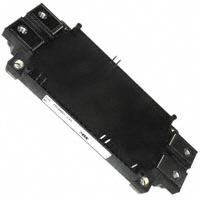
MITSUBISHI IGBT MODULES
CM200DX-24A
HIGH POWER SWITCHING USE
CM200DX-24A
¡IC ................................................................... 200A ¡VCES ......................................................... 1200V ¡Dual ¡Flatbase Type / Insulated Package / Copper (non-plating) base plate ¡RoHS Directive compliant
APPLICATION General purpose Inverters, Servo Amplifiers, Power supply, etc.
OUTLINE DRAWING & CIRCUIT DIAGRAM
152 137 121.7 110 ±0.5 99 94.5
Dimensions in mm
(7.4) 1.2
(20.5)
(4.2)
0.8
4-M6 NUTS
17 7
46 45 44 43 42 41 40 39 38 37 36 35 34 33 32 31 30 29 28 27 26 25
*58.4 (14) (14) 22 17 17 12 12 6 6
47
24
(3.81)
TERMINAL t = 0.8 φ4.3
(13.5)
(13.5)
39 50 ±0.5 57.5 62
1.15 0.65
23
48
1
2
3
4
5
6
7
8
9 10 11 12 13 14 15 16 17 18 19 20 21 22
6.5 (21.14)
A
*95 (102.25)
4-φ5.5 MOUNTING HOLES
(3) 13 SECTION A
*Pin positions with tolerance
*41.66 *45.48
3.5
0 (7.75)
*68.34 *72.14
*15 *18.8
(5.4) 12.5 (SCREWING DEPTH) 17 +1 -0.5
12.5
1.5
φ2.5 φ2.1
φ 0.5
LABEL
E2(39) G2(38) Tr2 E2(47) Di2 E1C2 (24)
Tolerance otherwise specified
Division of Dimension 0.5 to to to to to 3 6 30 120 400 Tolerance ±0.2 ±0.3 ±0.5 ±0.8 ±1.2
C1(48)
Di1 Tr1 Th
NTC
E1C2 (23)
over over over
3 6 30
G1(15) TH1(1) TH2(2) E1(16)
C1(22)
over 120
CIRCUIT DIAGRAM
Jan. 2009
�MITSUBISHI IGBT MODULES
CM200DX-24A
HIGH POWER SWITCHING USE
ABSOLUTE MAXIMUM RATINGS INVERTER PART
Symbol VCES VGES IC ICRM PC IE (Note.3) IERM(Note.3) Tj Tstg Viso — — — — Parameter Collector-emitter voltage Gate-emitter voltage
(Tj = 25°C, unless otherwise specified)
Conditions G-E Short C-E Short (Note. 1) DC, TC = 90°C Collector current (Note. 4) Pulse (Note. 1, 5) Maximum collector dissipation TC = 25°C (Note. 1) Emitter current TC = 25°C (Note. 4) (Free wheeling diode forward current) Pulse Junction temperature Storage temperature Isolation voltage Terminals to base plate, f = 60Hz, AC 1 minute (Note. 8) Base plate flatness On the centerilne X, Y Torque strength Main terminals M6 screw Torque strength Mounting M5 screw Weight (Typical)
Rating 1200 ±20 200 400 1250 200 400 –40 ~ +150 –40 ~ +125 2500 ±0 ~ +100 3.5 ~ 4.5 2.5 ~ 3.5 330
Unit V A W A °C Vrms μm N·m g
Note. 8: The base plate flatness measurement points are in the following figure.
Heat sink side
Y
+ –
+ convex : – concave :
X
–
+
Heat sink side
Jan. 2009 2
�MITSUBISHI IGBT MODULES
CM200DX-24A
HIGH POWER SWITCHING USE
ELECTRICAL CHARACTERISTICS INVERTER PART
Symbol ICES VGE(th) IGES VCE(sat) Cies Coes Cres QG td(on) tr td(off) tf trr (Note.3) Qrr (Note.3) Parameter
(Tj = 25°C, unless otherwise specified)
Conditions
VCE = VCES, VGE = 0V Collector cutoff current Gate-emitter threshold voltage IC = 20mA, VCE = 10V Gate leakage current ±VGE = VGES, VCE = 0V Collector-emitter saturation voltage Input capacitance Output capacitance Reverse transfer capacitance Total gate charge Turn-on delay time Turn-on rise time Turn-off delay time Turn-off fall time Reverse recovery time Reverse recovery charge IC = 200A, VGE = 15V IC = 200A, VGE = 15V VCE = 10V VGE = 0V VCC = 600V, IC = 200A, VGE = 15V VCC = 600V, IC = 200A VGE = ±15V, RG = 1.6Ω Inductive load (Note. 6) Tj = 25°C Tj = 125°C Chip (Note. 6)
(IE = 200A) IE = 200A, VGE = 0V (Note. 6) Tj = 25°C Tj = 125°C Chip
VEC(Note.3) Emitter-collector voltage Rlead Rth(j-c)Q Rth(j-c)R Rth(c-f) RGint RG
IE = 200A, VGE = 0V Module lead resistance Main terminals-chip, per switch Thermal resistance per IGBT (Note. 1) per free wheeling diode (Junction to case) Contact thermal resistance Thermal grease applied (Case to heat sink) (Note. 1) per 1 module Internal gate resistance TC = 25°C, per switch External gate resistance
Min. — 6 — — — — — — — — — — — — — — — — — — — — — — 1.6
Limits Typ. — 7 — 2.0 2.2 1.9 — — — 1000 — — — — — 8 2.6 2.16 2.5 1.6 — — 0.015 0 —
Max. 1 8 0.5 2.6 — — 35 3.0 0.68 — 130 100 450 600 150 — 3.4 — — — 0.10 0.19 — — 16
Unit mA V μA V
nF nC
ns
μC V mΩ K/W
(Note. 2)
Ω
NTC THERMISTOR PART
Symbol R ΔR/R B(25/50) P25
Note.1: 2: 3: 4: 5: 6:
Parameter Zero power resistance Deviation of resistance B constant Power dissipation
Conditions TC = 25°C TC = 100°C, R100 = 493Ω Approximate by equation TC = 25°C
(Note. 7)
Min. 4.85 –7.3 — —
Limits Typ. 5.00 — 3375 —
Max. 5.15 +7.8 — 10
Unit kΩ % K mW
Case temperature (TC), heat sink temperature (Tf) measured point is just under the chips. (Refer to the figure of the chip location.) Typical value is measured by using thermally conductive grease of λ = 0.9W/(m·K). IE, IERM, VEC, trr and Qrr represent ratings and characteristics of the anti-parallel, emitter-collector free wheeling diode (FWDi). Pulse width and repetition rate should be such that the device junction temperature (Tj) dose not exceed Tjmax rating. Junction temperature (Tj) should not increase beyond 150°C. Pulse width and repetition rate should be such as to cause negligible temperature rise. (Refer to the figure of the test circuit for VCE(sat) and VEC) 1 7: B(25/50) = In( R25 )/( 1 ) T50 R50 T25 R25: resistance at absolute temperature T25 [K]; T25 = 25 [°C]+273.15 = 298.15 [K] R50: resistance at absolute temperature T50 [K]; T50 = 50 [°C]+273.15 = 323.15 [K]
Jan. 2009 3
�MITSUBISHI IGBT MODULES
CM200DX-24A
HIGH POWER SWITCHING USE
Chip Location (Top view)
Dimensions in mm (tolerance: ±1mm)
(152) (121.7) (110) 0
46 45 44 43 42 41 40 39 38 37 36 35 34 33 32 31 30 29 28 27 26 25
0
16.2
47
Di 2
24
(62)
(50)
27.9 36.5
48
Tr2 Th
Di 1 Tr1
23
26.2 39.7
1
2
3
4
5
6
7
8
9 10 11 12 13 14 15 16 17 18 19 20 21 22
37.1
38.9
41.5
Each mark points the center position of each chip. Tr*: IGBT, Di*: FWDi, Th: NTC thermistor
76.6
LABEL SIDE
0
Jan. 2009 4
�MITSUBISHI IGBT MODULES
CM200DX-24A
HIGH POWER SWITCHING USE
C1
C1(C1s) C1(C1s)
C1 IC VGE = 0V
G1 E1(E1s)
V
VGE = 15V
G1 E1(E1s)
E1C2 VGE = 0V
G2 E2(E2s)
E1C2 VGE = 15V
G2 E2(E2s)
IC E2 Tr2
V
E2 Tr1 VCE(sat) test circuit
C1
C1(C1s) C1(C1s)
C1 IE VGE = 0V
G1 E1(E1s)
V
VGE = 0V
G1 E1(E1s)
E1C2 VGE = 0V
G2 E2(E2s)
E1C2 VGE = 0V
G2 E2(E2s)
IE E2 Di2
V
E2 Di1 VEC test circuit
Arm
IE 0V Load
VGE
90% 0%
IE trr
–VGE + +VGE 0V –VGE VCC IC 90% 0A t
RG VGE
VCE IC 0A td(on) tr td(off) tf Irr 10%
1/2 ✕ Irr Qrr = 1/2 ✕ Irr ✕ trr
Switching time test circuit and waveforms
trr, Qrr test waveform
Jan. 2009 5
�MITSUBISHI IGBT MODULES
CM200DX-24A
HIGH POWER SWITCHING USE
PERFORMANCE CURVES
OUTPUT CHARACTERISTICS (TYPICAL) Inverter part COLLECTOR-EMITTER SATURATION VOLTAGE CHARACTERISTICS (TYPICAL) Inverter part
COLLECTOR CURRENT IC (A)
VGE = 20V
15
COLLECTOR-EMITTER SATURATION VOLTAGE VCE(sat) (V)
400
Tj = 25°C 13
4 3.5 3 2.5 2 1.5 1 0.5 0 0
VGE = 15V
300 12 200 11 100 10 9 0 0 1 2 3 4 5 6 7 8 9 10
Tj = 25°C Tj = 125°C 100 200 300 400
COLLECTOR-EMITTER VOLTAGE VCE (V)
COLLECTOR CURRENT IC (A)
COLLECTOR-EMITTER SATURATION VOLTAGE CHARACTERISTICS (TYPICAL) Inverter part
FREE WHEELING DIODE FORWARD CHARACTERISTICS (TYPICAL) Inverter part 103
7 5 3 2
COLLECTOR-EMITTER SATURATION VOLTAGE VCE(sat) (V)
10
Tj = 25°C
8
6
EMITTER CURRENT IE (A)
102
7 5 3 2
4 IC = 400A 2 IC = 200A IC = 80A 0 6 8 10 12 14 16 18 20
101
Tj = 25°C Tj = 125°C 0 0.5 1 1.5 2 2.5 3 3.5 4
GATE-EMITTER VOLTAGE VGE (V)
EMITTER-COLLECTOR VOLTAGE VEC (V)
CAPACITANCE CHARACTERISTICS (TYPICAL) Inverter part 102
7 5 3 2
HALF-BRIDGE SWITCHING CHARACTERISTICS (TYPICAL) Inverter part 103
7 5 3 2
SWITCHING TIME (ns)
Cies
CAPACITANCE (nF)
tf td(off)
101
7 5 3 2
102
7 5 3 2
Coes
td(on) tr Conditions: VCC = 600V VGE = ±15V RG = 1.6Ω Tj = 125°C Inductive load
2 3 5 7 102 2 3 5 7 103
100
7 5 3 2
101
7 5 3 2
Cres VGE = 0V
10–1 –1 10 2 3 5 7 100 2 3 5 7 101 2 3 5 7 102 COLLECTOR-EMITTER VOLTAGE VCE (V)
100 1 10
COLLECTOR CURRENT IC (A)
Jan. 2009 6
�MITSUBISHI IGBT MODULES
CM200DX-24A
HIGH POWER SWITCHING USE
HALF-BRIDGE SWITCHING CHARACTERISTICS (TYPICAL) Inverter part 103
7 5 tf 3 2 td(off)
HALF-BRIDGE SWITCHING CHARACTERISTICS (TYPICAL) Inverter part 102
7
SWITCHING LOSS (mJ/pulse)
SWITCHING TIME (ns)
5 VGE = ±15V 3 RG = 1.6Ω 2
Conditions: VCC = 600V Tj = 125°C Inductive load
102 td(on) 7
5 3 2
tr Conditions: VCC = 600V VGE = ±15V IC = 200A Tj = 125°C Inductive load
2 3 5 7 101 2 3 5 7 102
101
7 5 3 2
Eoff Err Eon
2 3 5 7 102 2 3 5 7 103
101
7 5 3 2
100
100
100 1 10
GATE RESISTANCE RG (Ω)
COLLECTOR CURRENT IC (A) EMITTER CURRENT IE (A) REVERSE RECOVERY CHARACTERISTICS OF FREE WHEELING DIODE (TYPICAL) Inverter part 103
7 5 3 2
HALF-BRIDGE SWITCHING CHARACTERISTICS (TYPICAL) Inverter part 102
7
SWITCHING LOSS (mJ/pulse)
Eon
5 3 2
Irr trr
lrr (A), trr (ns)
Eoff
102
7 5 3 2
101 Conditions: VCC = 600V 3 VGE = ±15V IC, IE = 200A 2 Tj = 125°C Inductive load 100 0 10 23 5 7 101
5 7
Err
101
7 5 3 2
2
3
5 7 102
100 1 10
Conditions: VCC = 600V VGE = ±15V RG = 1.6Ω Tj = 25°C Inductive load
2 3 5 7 102 2 3 5 7 103
GATE RESISTANCE RG (Ω)
EMITTER CURRENT IE (A)
GATE CHARGE CHARACTERISTICS (TYPICAL) Inverter part 20
TRANSIENT THERMAL IMPEDANCE CHARACTERISTICS 100
7 Single pulse, 5 TC = 25°C 3 2 7 5 3 2
GATE-EMITTER VOLTAGE VGE (V)
IC = 200A VCC = 400V
15 VCC = 600V 10
NORMALIZED TRANSIENT THERMAL IMPEDANCE Zth(j–c)
10–1
10–2
7 5 3 2 Inverter IGBT part
5
0
0
200 400 600 800 1000 1200 1400 GATE CHARGE QG (nC)
10–3
: Per unit base = Rth(j–c) = 0.10K/W Inverter FWDi part : Per unit base = Rth(j–c) = 0.19K/W
10–52 3 5710–42 3 5710–32 3 5710–22 3 5710–12 3 57 100 2 3 57 101 TIME (s)
Jan. 2009 7
�
很抱歉,暂时无法提供与“CM200DX-24A”相匹配的价格&库存,您可以联系我们找货
免费人工找货