LANGUAGE
PRODUCT SPECIFICATION
【1.適用範囲
JAPANESE
ENGLISH
SCOPE】
本仕様書は、
殿 に納入する
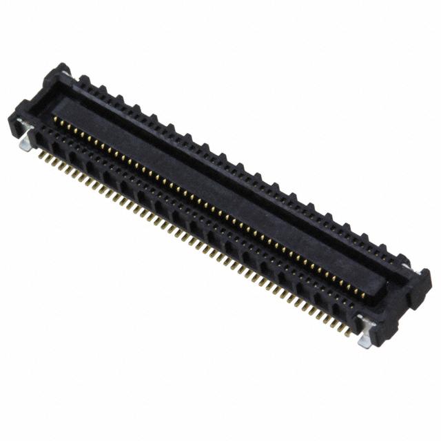
0.4 mm ピッチ 基板対基板 コネクタ
について規定する。
This specification covers the 0.4 mm PITCH BOARD TO BOARD CONNECTOR series.
【2.製品名称及び型番
PRODUCT NAME AND PART NUMBER】
製 品 名 称
Product Name
リセプタクル ハウジング アッセンブリ ネイル付
Receptacle Housing Assembly With Nail
リセプタクル ハウジング アッセンブリ エンボス梱包品
Receptacle Housing Assembly (Embossed Tape Package)
プラグ アッセンブリ ネイル付
Plug Assembly With Nail
プラグ アッセンブリ エンボス梱包品
Plug Assembly (Embossed Tape Package)
製 品 型 番
Part Number
500913-***8
500913-***2
55909-***3
55909-***4
* : 図面参照
REV.
A
B
C
D
E
SHEET
1~9
1~9
1~9
1~9
1~11
REVISE ON PC ONLY
F
変 更
REVISED
ECN No. J2016-0650
'15/12/15
N.SASAYAMA
REV.
DESCRIPTION
STATUS
DESIGN CONTROL
J
DOCUMENT NUMBER
PS-500913-001
Refer to the drawing.
F
1~15
TITLE:
0.4 BOARD TO BOARD CONNECTOR
(Hgt=1.8mm)
製品仕様書
THIS DOCUMENT CONTAINS INFORMATION THAT IS PROPRIETARY TO MOLEX ELECTRONIC
TECHNOLOGIES, LLC AND SHOULD NOT BE USED WITHOUT WRITTEN PERMISSION
WRITTEN BY:
CHECKED BY:
APPROVED BY:
R.SUMIYA
S.AIHARA
M.SASAO
DATE : YR/MO/DAY
2004/04/02
FILE NAME
PS-500913-001.docx
SHEET
1 OF 15
EN-037(2015-11 rev.1)
�LANGUAGE
PRODUCT SPECIFICATION
【3.定
格
項
RATINGS 】
目
Item
最大許容電圧
Rated Voltage (MAX.)
最大許容電流
Rated Current (MAX.)
*1
使用温度範囲
Ambient Temperature Range
JAPANESE
ENGLISH
規
格
Standard
50 V
[ AC (実効値 rms) / DC ]
0.3 A
-25°C
~
+ 85°C
*2
温度
-10°C ~ +50°C
Temperature
保管条件
湿度
85%R.H.以下(但し結露しないこと)
Storage Condition
Humidity
85%R.H. MAX. (No Condensation)
期間
出荷後 6ヶ月(未開封の場合)
Terms
For 6 months after shipping (unopened package)
*1 : 基板実装後の無通電状態は、使用温度範囲が適用されます。
Non-operating connectors after reflow must follow the operating temperature range condition.
*2 : 通電による温度上昇分も含む。
This includes the terminal temperature rise generated by conducting electricity.
REVISE ON PC ONLY
F
SEE SHEET 1 OF 15
REV.
DESCRIPTION
TITLE:
0.4 BOARD TO BOARD CONNECTOR
(Hgt=1.8mm)
製品仕様書
THIS DOCUMENT CONTAINS INFORMATION THAT IS PROPRIETARY TO MOLEX ELECTRONIC
TECHNOLOGIES, LLC AND SHOULD NOT BE USED WITHOUT WRITTEN PERMISSION
DOCUMENT NUMBER
FILE NAME
SHEET
PS-500913-001
PS-500913-001.docx
2 OF 15
EN-037(2015-11 rev.1)
�LANGUAGE
PRODUCT SPECIFICATION
【4.性
能
JAPANESE
ENGLISH
PERFORMANCE 】
4-1.電気的性能
項
Electrical Performance
目
条
Item
接 触 抵 抗
Contact
Resistance
4-1-1
絶 縁 抵 抗
Insulation
Resistance
4-1-2
耐 電 圧
Dielectric
Strength
4-1-3
4-2. 機械的性能
項
件
Test Condition
コネクタを嵌合させ、開放電圧 20mV以下、短絡電流
10mA にて測定する。
(JIS C5402 5.4)
規
格
Requirement
40 milliohms MAX.
Mate connectors and measured by dry circuit,
20mV MAX., 10mA.
(JIS C5402 5.4)
コネクタを嵌合させ、隣接するターミナル間及び
タ-ミナル、アース間に、DC 250V を印加し測定する。
(JIS C5402 5.2/MIL-STD-202 試験法 302)
100 Megohms MIN.
Mate connectors and apply 200V DC between adjacent
terminal or ground.
(JIS C5402 5.2/MIL-STD-202 Method 302)
コネクタを嵌合させ、隣接するタ-ミナル間及び
タ-ミナル、アース間に、AC(rms) 250V (実効値) を
1分間 印加する。
(JIS C5402 5.1/MIL-STD-202 試験法 301)
異状なきこと
No Breakdown
Mate connectors and apply 250V AC(rms) for 1 minute
between adjacent terminal or ground.
(JIS C5402 5.1/MIL-STD-202 Method 301)
Mechanical Performance
目
条
Item
4-2-1
挿入力及び抜去力
Insertion and
Withdrawal Force
4-2-2
ターミナル保持力
Terminal / Housing
Retention Force
件
Test Condition
毎分 25±3mm の速さで挿入、抜去を行う。
Insert and withdraw connectors at the speed rate of
25±3 mm/minute.
ハウジングに装着されたターミナルを
毎分 25±3mm の速さで引張る。
Apply axial pull out force at the speed rate of
25±3 mm/minute on the terminal assembled in the
housing.
REVISE ON PC ONLY
F
SEE SHEET 1 OF 15
REV.
DESCRIPTION
規
格
Requirement
第6項参照
Refer to paragraph 6
0.49N {0.05 kgf} MIN.
TITLE:
0.4 BOARD TO BOARD CONNECTOR
(Hgt=1.8mm)
製品仕様書
THIS DOCUMENT CONTAINS INFORMATION THAT IS PROPRIETARY TO MOLEX ELECTRONIC
TECHNOLOGIES, LLC AND SHOULD NOT BE USED WITHOUT WRITTEN PERMISSION
DOCUMENT NUMBER
FILE NAME
SHEET
PS-500913-001
PS-500913-001.docx
3 OF 15
EN-037(2015-11 rev.1)
�LANGUAGE
PRODUCT SPECIFICATION
4-3.そ
の
他
項
Environmental Performance and Others
目
条
Item
繰返し挿抜
Repeated
Insertion /
Withdrawal
4-3-1
温 度 上 昇
Temperature Rise
4-3-2
耐 振 動 性
Vibration
4-3-3
耐 衝 撃 性
Mechanical Shock
4-3-4
耐 熱 性
Heat Resistance
4-3-5
件
Test Condition
1分間 10回 以下 の速さで挿入、抜去を
30回 繰返す。
When mated up to 30 cycles repeatedly by
the rate of 10 cycles per minute.
コネクタを嵌合させ、最大許容電流を
通電し、コネクタの温度上昇分を測定する。
(UL 498)
Carrying rated current load.
(UL 498)
DC 1mA 通電状態にて、嵌合軸を含む互いに
垂直な 3方向 に掃引割合に
10~55~10 Hz/分、全振幅 1.5mm の振動を
各2時間 加える。
(MIL-STD-202 試験法 201)
Amplitude
: 1.5mm P-P
Frequency : 10~55~10 Hz in 1 minute.
Duration
: 2 hours in each X.Y.Z.axes.
(MIL-STD-202 Method 201)
DC 1mA 通電状態にて、嵌合軸を含む互いに
垂直な 6方向 に 490m/s2 { 50G } の衝撃
を 各3回 加える。
(JIS C60068-2-27/MIL-STD-202 試験法 213)
490m/s2 { 50G } , 3 strokes in each X.Y.Z.
axes.
(JIS C60068-2-27/MIL-STD-202 Method 213)
コネクタを嵌合させ、85±2°C の雰囲気中に
96時間 放置後取り出し、1~2時間 室温に放
置する。
(JIS C60068-2-2/MIL-STD-202 試験法 108)
85±2°C, 96 hours
(JIS C60068-2-2/MIL-STD-202 Method 108)
耐 寒 性
Cold Resistance
4-3-6
JAPANESE
ENGLISH
コネクタを嵌合させ、–25±3°C の雰囲気中
に 96時間 放置後取り出し、1~2時間 室温に
放置する。 (JIS C60068-2-1)
–25±3°C, 96 hours
REVISE ON PC ONLY
F
SEE SHEET 1 OF 15
REV.
DESCRIPTION
(JIS C60068-2-1)
規
格
Requirement
接 触 抵 抗
Contact
Resistance
80 milliohms MAX.
温 度 上 昇
Temperature
Rise
30 °C MAX.
外
観
Appearance
異状なきこと
No Damage
接 触 抵 抗
Contact
Resistance
80 milliohms MAX.
瞬
断
Discontinuity
1 microsecond
MAX.
外
観
Appearance
異状なきこと
No Damage
接 触 抵 抗
Contact
Resistance
80 milliohms MAX.
瞬
断
Discontinuity
1 microsecond
MAX.
外
観
Appearance
異状なきこと
No Damage
接 触 抵 抗
Contact
Resistance
80 milliohms MAX.
外
観
Appearance
異状なきこと
No Damage
接 触 抵 抗
Contact
Resistance
80 milliohms MAX.
TITLE:
0.4 BOARD TO BOARD CONNECTOR
(Hgt=1.8mm)
製品仕様書
THIS DOCUMENT CONTAINS INFORMATION THAT IS PROPRIETARY TO MOLEX ELECTRONIC
TECHNOLOGIES, LLC AND SHOULD NOT BE USED WITHOUT WRITTEN PERMISSION
DOCUMENT NUMBER
FILE NAME
SHEET
PS-500913-001
PS-500913-001.docx
4 OF 15
EN-037(2015-11 rev.1)
�LANGUAGE
PRODUCT SPECIFICATION
項
目
条
Item
温度サイクル
Temperature
Cycling
4-3-8
塩 水 噴 霧
Salt Spray
4-3-9
亜硫酸ガス
SO2 Gas
4-3-10
件
コ ネ クタ を嵌 合さ せ、 40±2°C 、 相 対 湿度
90~95% の雰囲気中に 96時間 放置後
取り出し、1 ~2時間 室温に放置する。
(JIS C60068-2-3/MIL-STD-202 試験法 103)
Temperature
: 40±2°C
Relative Humidity : 90~95%
Duration
: 96 hours
(JIS C60068-2-3/MIL-STD-202 Method 103)
コネクタを嵌合させ、 –55°C に 30分、
+85°C に 30分 これを 1サイクル とし、
5サイクル 繰返す。但し、温度移行時間は
5分以内 とする。試験後 1~2時間 室温に
放置する。
(JIS C0025)
5 cycles of :
a) – 55°C
30 minutes
b) + 85°C
30 minutes
(JIS C0025)
コネクタを嵌合させ、35±2°C にて 5±1%
重量比 の塩水を 48±4時間 噴霧し、試験後
常温で水洗いした後、室温で乾燥させる。
(JIS C60068-2-11/MIL-STD-202 試験法101)
48±4 hours exposure to a salt spray from the
5±1% solution at 35±2°C.
(JIS C60068-2-11/MIL-STD-202 Method 101)
コネクタを嵌合させ、40±2℃ にて
50±5ppm の亜硫酸ガス中に 24時間
放置する。
24 hours exposure to 50±5ppm SO2 gas
at 40±2℃.
半田付け性
Solderability
4-3-11
規
格
Requirement
Test Condition
耐 湿 性
Humidity
4-3-7
JAPANESE
ENGLISH
ターミナルまたはピンをフラックスに浸し、
245±5°C の半田に 2~3秒 浸す。
Soldering Time
: 2~3 sec.
Solder Temperature : 245±5 °C
REVISE ON PC ONLY
F
SEE SHEET 1 OF 15
REV.
DESCRIPTION
外
観
Appearance
接 触 抵 抗
Contact
Resistance
耐 電 圧
Dielectric
Strength
絶 縁 抵 抗
Insulation
Resistance
異状なきこと
No Damage
80 milliohms MAX.
4-1-3項満足のこと
Must meet 4-1-3
50 Megohms MIN.
外
観
Appearance
異状なきこと
No Damage
接 触 抵 抗
Contact
Resistance
80 milliohms MAX.
外
観
Appearance
異状なきこと
No Damage
接 触 抵 抗
Contact
Resistance
80 milliohms MAX.
外
観
Appearance
異状なきこと
No Damage
接 触 抵 抗
Contact
Resistance
80 milliohms MAX.
濡れ性
Solder
Wetting
浸漬面積の
95%以上
95% of immersed
area must show
no voids, pin
holes.
TITLE:
0.4 BOARD TO BOARD CONNECTOR
(Hgt=1.8mm)
製品仕様書
THIS DOCUMENT CONTAINS INFORMATION THAT IS PROPRIETARY TO MOLEX ELECTRONIC
TECHNOLOGIES, LLC AND SHOULD NOT BE USED WITHOUT WRITTEN PERMISSION
DOCUMENT NUMBER
FILE NAME
SHEET
PS-500913-001
PS-500913-001.docx
5 OF 15
EN-037(2015-11 rev.1)
�LANGUAGE
PRODUCT SPECIFICATION
項
目
JAPANESE
ENGLISH
条
Item
リフロー時
件
Test Condition
Reflow soldering method
規
格
Requirement
第7項参照。
半田耐熱性
Resistance to
Soldering Heat
4-3-12
See paragraph 7
手半田時
端子先端より0.2mm、金具先端より0.2mmの
位置まで350±10℃の半田ゴテにて最大5秒
外
観
加熱する。但し、ピンに異常な加圧がないこ Appearance
と。
Soldering iron method
Using a soldering iron (350±10℃ for 5
seconds MAX.) heat up the area 0.2mm from
the tip of the solder tails and fitting nails.
However, do not apply excessive pressure to
either the terminals or fitting nails.
(
) :参考規格
{
} :参考単位
【5.外観形状、寸法及び材質
図面参照
端子ガタ、割れ等
異状なきこと
No Damage
Reference Standard
Reference Unit
PRODUCT SHAPE, DIMENSIONS AND MATERIALS】
Refer to the drawing.
REVISE ON PC ONLY
F
SEE SHEET 1 OF 15
REV.
DESCRIPTION
TITLE:
0.4 BOARD TO BOARD CONNECTOR
(Hgt=1.8mm)
製品仕様書
THIS DOCUMENT CONTAINS INFORMATION THAT IS PROPRIETARY TO MOLEX ELECTRONIC
TECHNOLOGIES, LLC AND SHOULD NOT BE USED WITHOUT WRITTEN PERMISSION
DOCUMENT NUMBER
FILE NAME
SHEET
PS-500913-001
PS-500913-001.docx
6 OF 15
EN-037(2015-11 rev.1)
�LANGUAGE
PRODUCT SPECIFICATION
【6.挿入力及び抜去力
JAPANESE
ENGLISH
INSERTION/WITHDRAWAL FORCE】
N
{kgf}
挿入力(最大値)
Insertion (MAX.)
初回
6回目
30回目
1st
6th
30th
28.3
28.3
28.3
{2.9}
{2.9}
{2.9}
抜去力(最小値)
Withdrawal (MIN.)
初回
6回目
30回目
1st
6th
30th
4.7
4.7
4.7
{0.48}
{0.48}
{0.48}
30
N
{kgf}
35.3
{3.6}
35.3
{3.6}
35.3
{3.6}
5.88
{0.6}
5.88
{0.6}
5.88
{0.6}
40
N
{kgf}
47.1
{4.8}
47.1
{4.8}
47.1
{4.8}
7.84
{0.8}
7.84
{0.8}
7.84
{0.8}
50
N
{kgf}
58.8
{6.0}
58.8
{6.0}
58.8
{6.0}
9.80
{1.0}
9.80
{1.0}
9.80
{1.0}
60
N
{kgf}
70.6
{7.2}
70.6
{7.2}
70.6
{7.2}
11.7
{1.20}
11.7
{1.20}
11.7
{1.20}
70
N
{kgf}
82.4
{8.4}
82.4
{8.4}
82.3
{8.4}
13.7
{1.40}
13.7
{1.40}
13.7
{1.40}
90
N
{kgf}
105.9
{10.8}
105.9
{10.8}
105.9
{10.8}
17.6
{1.8}
17.6
{1.8}
17.6
{1.8}
100
N
{kgf}
117.6
{12.0}
117.6
{12.0}
117.6
{12.0}
19.6
19.6
19.6
{2.0}
{2.0}
{2.0}
} : 参考単位
Reference Unit
極 数
No. of
CKT
単位
UNIT
24
{
REVISE ON PC ONLY
F
SEE SHEET 1 OF 15
REV.
DESCRIPTION
TITLE:
0.4 BOARD TO BOARD CONNECTOR
(Hgt=1.8mm)
製品仕様書
THIS DOCUMENT CONTAINS INFORMATION THAT IS PROPRIETARY TO MOLEX ELECTRONIC
TECHNOLOGIES, LLC AND SHOULD NOT BE USED WITHOUT WRITTEN PERMISSION
DOCUMENT NUMBER
FILE NAME
SHEET
PS-500913-001
PS-500913-001.docx
7 OF 15
EN-037(2015-11 rev.1)
�LANGUAGE
PRODUCT SPECIFICATION
【7.赤外線リフロー条件
JAPANESE
ENGLISH
INFRARED REFLOW CONDITION 】
250℃以下(ピーク温度)
250℃ MAX.(PEAK TEMP.)
230℃以上 30±10秒
230℃ MIN. 30±10sec.
予熱 150~180秒
90 ± 30 秒
Pre-heat 150~180℃
90±30 sec
温度条件グラフ
TEMPERATURE CONDITION GRAPH
(基板表面温度)
(TEMPERATURE ON BOARD PATTERN SIDE)
注記:本リフロー条件に関しては、リフロー装置及び基板などにより条件が異なりますので
事前に実装評価(リフロー評価)の御確認を御願い致します。
NOTE : Please check the mount condition (reflow soldering condition) by your own devices beforehand,
because the condition changes by the soldering devices, p.c.boards, and so on.
推奨ランド寸法:SDをご参照ください
参考メタルマスク厚さ:t=0.12[mm]
参考メタルマスク開口率:100%(大気リフロー時)
Recommended land dimension: Please refer to the SD.
Reference Metal mask thickness: t = 0.12[mm].
Reference Metal mask aperture rate: 100% (at air reflow).
REVISE ON PC ONLY
F
SEE SHEET 1 OF 15
REV.
DESCRIPTION
TITLE:
0.4 BOARD TO BOARD CONNECTOR
(Hgt=1.8mm)
製品仕様書
THIS DOCUMENT CONTAINS INFORMATION THAT IS PROPRIETARY TO MOLEX ELECTRONIC
TECHNOLOGIES, LLC AND SHOULD NOT BE USED WITHOUT WRITTEN PERMISSION
DOCUMENT NUMBER
FILE NAME
SHEET
PS-500913-001
PS-500913-001.docx
8 OF 15
EN-037(2015-11 rev.1)
�LANGUAGE
PRODUCT SPECIFICATION
【8.取り扱い上の注意事項
JAPANESE
ENGLISH
INSTRUCTION UPON USAGE 】
[嵌合]
嵌合は極力嵌合軸に沿って平行に行って下さい。(図-1)
その際、リセハウジングとプラグの内壁同士を合せる様に位置決めした後に押し込み嵌合して下さい。
斜めの嵌合になる場合は10°以下の角度でリセハウジングとプラグの内壁同士を軽く当て、位置決めした
後に嵌合して下さい。(図-2)
尚、リセハウジングの外壁とプラグ外壁とを当てた(支点とした)状態で嵌合を行いますと、反支点側の
リセハウジングとプラグの内壁同士が干渉し、ハウジングが破壊する恐れが有りますのでこのような嵌合は
お避け下さい。(図-3)
Please mate the connector with parallel manner. (Figure-1)
Please locate the inside wall of the rec housing and the plug after mating.
In the case of skew mating, please do not mate the connector at more than 10°lead
in angle . (Figure-2)
Please do not mate the rec and plug at an angle as this way, Cause the housing is broken.
(Figure-3)
[抜去]
抜去は極力嵌合軸に沿って平行に行って下さい。(図-1)
または、左右に少しづつ振りながら行って下さい。(図-4)
(過度のこじり抜去には注意して下さい。ハウジングの破壊およびピン損傷の原因となります。)(図-5)
[Withdrawal]
Withdraw the connector parallel to mating axis as much as possible (Figure-1).
Or do it with slightly swinging them right to left. (Figure-4)
(Please take care NOT to do excess twist extraction. It could cause the housing or pin breakage.) (Figure-5)
REVISE ON PC ONLY
F
SEE SHEET 1 OF 15
REV.
DESCRIPTION
TITLE:
0.4 BOARD TO BOARD CONNECTOR
(Hgt=1.8mm)
製品仕様書
THIS DOCUMENT CONTAINS INFORMATION THAT IS PROPRIETARY TO MOLEX ELECTRONIC
TECHNOLOGIES, LLC AND SHOULD NOT BE USED WITHOUT WRITTEN PERMISSION
DOCUMENT NUMBER
FILE NAME
SHEET
PS-500913-001
PS-500913-001.docx
9 OF 15
EN-037(2015-11 rev.1)
�LANGUAGE
PRODUCT SPECIFICATION
REVISE ON PC ONLY
F
SEE SHEET 1 OF 15
REV.
DESCRIPTION
JAPANESE
ENGLISH
TITLE:
0.4 BOARD TO BOARD CONNECTOR
(Hgt=1.8mm)
製品仕様書
THIS DOCUMENT CONTAINS INFORMATION THAT IS PROPRIETARY TO MOLEX ELECTRONIC
TECHNOLOGIES, LLC AND SHOULD NOT BE USED WITHOUT WRITTEN PERMISSION
DOCUMENT NUMBER
FILE NAME
SHEET
PS-500913-001
PS-500913-001.docx
10 OF 15
EN-037(2015-11 rev.1)
�LANGUAGE
PRODUCT SPECIFICATION
【9.その他
注意事項
JAPANESE
ENGLISH
OTHER】
・外観について
1. 本製品の樹脂部に黒点、多少の傷、微小な気泡等が生じることがありますが、性能上問題ありません。{また、本製品
のモールド材料は LCP を使用しているため、ウェルドラインが目立つ場合がありますが、製品性能には影響ないもの
です。}
Although this product may have a small black dot, a weld line or a scratch on the housing, it doesn't impact
the product’s performance. {Also, although weld line may stand out due to LCP used to mold material of this
product, it doesn't impact the product’s performance.}
2. 成形品の色相に多少の違いを生じる場合がありますが、製品性能には影響ありません。
Although there may be slight differences in the housing color tone, it doesn't impact the product’s
performance.
3. 本製品の錫めっきを使用しているため、外観に摺動痕がつく場合が御座いますが、製品性能に影響はありません。
Although the surface of the product could have scratch marks by frictions because of the Tin plating, it doesn't
impact the product’s performance.
・実装について
4
本リフロー条件に関しては、実装条件(大気/N2リフロー、温度プロファイル、半田ペースト、メタルマスク板厚・開口
率、基板パターンレイアウト、実装基板種別などの種々の要素)により条件が異なりますので、必ずご使用前に、顧客
様のご使用環境で事前に実装評価(リフロー評価) を実施願います。実装条件によっては、接点部への半田上がりや
フラックス上りが発生するなど製品性能に影響を及ぼす場合があります。
Please make sure to do test run under the mounting condition (reflow soldering condition) on your own devices
before use because reflow condition may change due to the local condition (Air / N2 reflow / temperature profile
/ solder paste, metal mask thickness / aperture rate / pattern layout of PWB / types of PWB / and other factors ).
Depending on the mounting condition, product's performance might be influenced by occurrence of
solder-wicking or flux wicking at contact area.
5. 本製品の一般性能確認はリジット基板にて実施しております。フレキシブル基板等の特殊な基板へ実装する場合は、
事前に実装確認等を行った上でご使用願います。
The product performance was tested using rigid PWB. In case the product needs to be mounted onto FPC,
please conduct a reflow test on the FPC before use.
6. フレキシブル基板に実装する場合は、基板の変形を防止するため、補強板をご使用願います。
In case of mounting the connector onto FPC, add a stiffener on the FPC in order to prevent the deformation.
7. 弊社の推奨基板パターン寸法を変更して設計を行なう際は、致命的な不良の原因にもなりますので、あらかじめご相
談ください。
In case of designing with changing our recommended board pattern size, please consult the contact person in
advance because it may cause a fatal defect.
8. 実装性能(平坦度)は、実装基板の反りの影響を含まないものと致します。基板の反りはコネクタ両端部を基準とし、コ
ネクタ中央部にて Max0.02mm として下さい。
The mounting specification for coplanarity does not include the influence of warpage of the PWB. Warpage of
the PWB should be 0.02mm at maximum at center of the connector based on the both sides of connector.
REVISE ON PC ONLY
F
SEE SHEET 1 OF 15
REV.
DESCRIPTION
TITLE:
0.4 BOARD TO BOARD CONNECTOR
(Hgt=1.8mm)
製品仕様書
THIS DOCUMENT CONTAINS INFORMATION THAT IS PROPRIETARY TO MOLEX ELECTRONIC
TECHNOLOGIES, LLC AND SHOULD NOT BE USED WITHOUT WRITTEN PERMISSION
DOCUMENT NUMBER
FILE NAME
SHEET
PS-500913-001
PS-500913-001.docx
11 OF 15
EN-037(2015-11 rev.1)
�LANGUAGE
PRODUCT SPECIFICATION
JAPANESE
ENGLISH
9. 本製品は大気リフローでの実装を想定しています。N2 リフローで実装した場合、リフロー後、半田上がりを生じる恐れ
があります。N2 リフローでの実装をお考えの場合、別途評価が必要になります。
This product is designed to be mounted by air reflow. So, if this product is mounted by N2 reflow, solder wicking
may caused after reflow. Therefore if it is plan to adopt N2 reflow for this connector, an evaluation is needed
separately.
10. 弊社評価では本仕様書記載の推奨条件に基づき評価を実施しています。
Our evaluation is conducted based on Molex-recommended condition specified in this product specification.
11. 本製品の平坦度については、実装前での保証のみであり、実装中および実装後での平坦度については、保証の限り
ではありません。
Only coplanarity before reflow is guaranteed. Coplanarity in and after reflow is not guaranteed.
12. 本製品は端子先端部に、カット面がある為に端子先端部の実装性(基板への半田付け性)は、端子側面・後側に比べ
て悪くなります。しかし、側面及び後側においてフィレットが形成されていれば、機能及び強度に問題はありません。
The solderability of the terminal tip, which is cut surface without plating, is worse than the sides/back of the
terminal with plating. However, it will not impact the product's function or the retention force if good soldering
fillet is formed at the sides/back of the terminal.
13. 半田実装部の未半田は、ターミナル脱落、ピン間ショート、ターミナル座屈、またコネクタの基板からの外れが懸念さ
れます。従って全てのターミナルテール部及び、ネイル部に半田付けを行って下さい。
If you leave any soldering area on this product open, it could occur terminal disengagement, short circuit
between pins, terminal buckling or connector disengagement from the PWB. Therefore, please solder all of the
soldering tails and fitting nails on the PWB.
14. 本製品は低背の為、端子コンタクト部以外の場所へフラックス上りが発生することがありますが、製品性能には影響
ありません。
Since this product is low profile product, flux wicking could be occurred on the areas except for the terminal
contacts. However it does not impact on the product’s performance.
15. 実装機によってコネクタに負荷が加わると変形、破損する場合がありますので事前にご確認下さい。
If accidental contact is added onto connectors in the reflow machine, connectors could be deformed or
damaged. Therefore review the reflow machine before use of the connectors.
16. リフロー条件によっては、樹脂部の変色や端子めっき部にヨリが発生する場合がありますが、製品性能に影響はござ
いません。
Although color tone of housing or surface of terminal plating could be varied depending on reflow conditions, it
does not impact on the product’s performance.
17. リフロー後、半田付け部に変色が見られることがありますが、製品性能に影響はありません。
Although some discoloration could be seen on the soldering tail after reflow, it does not impact on the
product’s performance.
・製品の仕様について
18. 本製品をご使用時には、1PIN 当りの定格以上の電流を複数の回路に分岐しての使用は避けて下さい。
When using this product, ensure that the specification for rated current per a circuit is followed. Do not allow the
sum of the current used on several circuits to exceed the maximum allowable current.
REVISE ON PC ONLY
F
SEE SHEET 1 OF 15
REV.
DESCRIPTION
TITLE:
0.4 BOARD TO BOARD CONNECTOR
(Hgt=1.8mm)
製品仕様書
THIS DOCUMENT CONTAINS INFORMATION THAT IS PROPRIETARY TO MOLEX ELECTRONIC
TECHNOLOGIES, LLC AND SHOULD NOT BE USED WITHOUT WRITTEN PERMISSION
DOCUMENT NUMBER
FILE NAME
SHEET
PS-500913-001
PS-500913-001.docx
12 OF 15
EN-037(2015-11 rev.1)
�LANGUAGE
PRODUCT SPECIFICATION
JAPANESE
ENGLISH
19. 本製品をご使用時に取り付けられた電線・プリント基板の共振や、機器の回転構造や可動部分の動作によりコネクタ
嵌合部(接点部)が常に動いてしまう状態での御使用は避けて下さい。接触部の摺動磨耗等による 接触不良の原因
となります。 従って、機器内で電線・プリント基板を固定し、共振を抑える等の処置をお願い致します。
Do not use the connector in a condition where the mating area (contact area) are constantly moved due to
sympathetic vibration of wires and PWB or constant movement of devices. It may cause contact failure due to
the worn out. Therefore fix wires and PWB on the chassis to reduces sympathetic vibration.
20. コネクタに外力が加わらないようにクリアランスをあけた筐体構造にして下さい。
Keep enough clearance between connector and chassis of your application in order to avoid pressure on the
connector.
21. 本製品を結露・水濡れが発生する環境でのご使用の場合は、適切な防滴処置をお願い致します。結露・水濡れにより、
回路間で絶縁不良を起こす可能性が御座います。
When using this product in an environment where dew condensation and water wetting occur, apply an
appropriate drip-proof treatment. Dew condensation and water wetting could cause insulation failure between
the circuits.
22. コネクタのみで基板を支えることは避け、コネクタ以外での基板固定対策を行ってください。
Avoid using a connector alone to mechanically support the PWB. Adopt separate fixture to support PWB
besides the connector in the chassis.
23. 活電状態の電気回路で、挿入、抜去ができることを前提に作られていません。スパーク等による危険の発生、性能不
良につながりますので、活電状態での挿入、抜去はしないで下さい。
Do not mate and un-mate connectors while those are energized since this connector is not designed to allow it.
It may cause danger due to sparks and functional failure of the product.
24. 一枚の基板にコネクタを複数実装する場合は、嵌合相手側はそれぞれ個別の基板に実装してご使用を願います。
When mounting several board to board connectors on a same PWB, ensure to mount the each mating
connector on a separate PWB.
25. 本製品及び加工工程品(仕掛品)や加工品(ハーネス品)の梱包及び輸送・保管時において、コネクタ間での絡みや衝
撃、積み重ね等による負荷が掛からないようにして下さい。変形・破損等による性能不良の原因となります。
At packaging, transportation and storing, avoid applying loads to connectors by handling, interference of
connectors or piling-up packages. It could cause functional defect such as connector deformation or breakage.
26. 推奨保管条件での保管をお願い致します。もし、梱包品の推奨保管条件を超えてしまった場合は外観、半田付け性を
確認の上ご使用ください。
Store the products under recommended storage condition. If the recommended storage conditions of the
packaging is exceeded, check the appearance of the products and solder-wettability before use.
27. 基板実装後に基板を直接積み重ねない様に注意してください。
Do not stack PWB directly after mounting the connector on it.
28. コネクタの性能を損なう恐れがある為、コネクタの洗浄は、行わないで下さい。
Do not wash connector because it may impact the product’s function.
REVISE ON PC ONLY
F
SEE SHEET 1 OF 15
REV.
DESCRIPTION
TITLE:
0.4 BOARD TO BOARD CONNECTOR
(Hgt=1.8mm)
製品仕様書
THIS DOCUMENT CONTAINS INFORMATION THAT IS PROPRIETARY TO MOLEX ELECTRONIC
TECHNOLOGIES, LLC AND SHOULD NOT BE USED WITHOUT WRITTEN PERMISSION
DOCUMENT NUMBER
FILE NAME
SHEET
PS-500913-001
PS-500913-001.docx
13 OF 15
EN-037(2015-11 rev.1)
�LANGUAGE
PRODUCT SPECIFICATION
JAPANESE
ENGLISH
・製品操作について
29. 基板実装前後に端子、補強金具に触らないでください。
Do not touch the terminals and fitting nails of connectors before or after mounting onto the PWB.
30. 嵌合後、コネクタピッチ方向、スパン方向及び回転方向への負荷がかかるような動作またはセットはしないでください。
コネクタ破壊やはんだクラックを引き起こします。
Avoid move or assembly of connector which could apply loads to the direction of the connector pitch, span or
rotation. It may damage the connector and crack the soldering.
31. 嵌合の際、嵌合が不十分にならないようにご注意下さい。また、セットへの組み込み後も、振動、衝撃等で嵌合の浮き
が発生しないような状態にて使用してください。
Ensure to mate connectors fully. Also mount and assemble the connector in your application unit with
disengagement proof to avoid connector disengagement due to vibration or shocks.
・リペアについて
32. 実装後において半田こてによる手修正を行う際は、必ず仕様書掲載の条件以内で行って下さい。条件を超えて実施し
た場合、端子の抜け、接点ギャップの変化、モールドの変形、溶融等、破損の原因になります。
When conducting manual repairs using a soldering iron, follow the soldering conditions shown in the product
specification. If the conditions in the product specification are not followed, it may cause the terminal
disengagement, contact gap change, housing deformation, housing melting, and connector damage.
33. 半田こてによる手修正を行なう際、過度の半田やフラックスを使用しないで下さい。半田上がりやフラックス上がりによ
り接触、機能不良に至る場合があります。
When conducting manual repairs using a soldering iron, do not use excess solder and flux than needed. It may
cause solder wicking and flux wicking issues, and also eventually cause a contact defect and functional issues.
9.環境指令への適合
COMPLIANCE WITH ENVIRONMENTAL DIRECTIVE 】
1. ELV及びRoHS適合品
ELV and RoHS Compliant.
REVISE ON PC ONLY
F
SEE SHEET 1 OF 15
REV.
DESCRIPTION
TITLE:
0.4 BOARD TO BOARD CONNECTOR
(Hgt=1.8mm)
製品仕様書
THIS DOCUMENT CONTAINS INFORMATION THAT IS PROPRIETARY TO MOLEX ELECTRONIC
TECHNOLOGIES, LLC AND SHOULD NOT BE USED WITHOUT WRITTEN PERMISSION
DOCUMENT NUMBER
FILE NAME
SHEET
PS-500913-001
PS-500913-001.docx
14 OF 15
EN-037(2015-11 rev.1)
�LANGUAGE
PRODUCT SPECIFICATION
REV.
REV. RECORD
新規作成
A
JAPANESE
ENGLISH
DATE
ECN NO.
WRITTEN BY :
CHECKED BY :
RELEASED
'04/04/02
J2004-3540
R.SUMIYA
S.AIHARA
B
変
更
REVISED
'04/08/02
J2005-0342
Y.SAKIYAMA
M.SASAO
C
変
更
REVISED
'04/09/03
J2005-0661
R.SUMIYA
H.HIRATA
D
変
更
REVISED
'06/02/06
J2006-2490
N.AIDA
K.TOYODA
E
変
更
REVISED
'07/02/23
J2007-2417
M.NABEI
K.TOYODA
F
変
更
REVISED
'15/12/15
J2016-0650
N.SASAYAMA
T.ASAKAWA
REVISE ON PC ONLY
F
SEE SHEET 1 OF 15
REV.
DESCRIPTION
TITLE:
0.4 BOARD TO BOARD CONNECTOR
(Hgt=1.8mm)
製品仕様書
THIS DOCUMENT CONTAINS INFORMATION THAT IS PROPRIETARY TO MOLEX ELECTRONIC
TECHNOLOGIES, LLC AND SHOULD NOT BE USED WITHOUT WRITTEN PERMISSION
DOCUMENT NUMBER
FILE NAME
SHEET
PS-500913-001
PS-500913-001.docx
15 OF 15
EN-037(2015-11 rev.1)
�