mEZD71202A Series
4.5V - 24V Input, 2A, DC/DC Power Supply
FEATURES
4.5V to 24V Wide Operating Input
2A Load Current
Hiccup Short-Circuit Protection
Over-/Under-Voltage Protection
Over-Current Protection
Over-Temperature Protection
Open Design Files and BOM
ORDERING INFORMATION
Input Voltage
(V)
A - F: 4.5 - 24
G: 6.5 - 24
Part Number
MEZD71202A-X
Output Voltage
(V)
1, 1.2, 1.5, 1.8,
2.5, 3.3, 5
Output Current
(A)
2
Output Voltage Options
Manufacture Yourself Available
A = 1.0V
E = 2.5V
Design Files Available for Manufacture
Power Derating
120
Natural Convection
100
Output Power (%)
C = 1.5V
G = 5.0V
D = 1.8V
mEZD712xx FAMILY PRODUCTS
VIN = 12V, VOUT = 3.3V and 5V
Part Number
Input Voltage
(V)
mEZD71201A-X
4.5 - 24
mEZD71202A-X
4.5 - 24
mEZD71203A-X
5 - 16
mEZD71210A-X
4.5 - 17
80
60
VOUT=3.3V
40
B = 1.2V
F = 3.3V
Output Voltage
(V)
1, 1.2, 1.5, 1.8,
2.5, 3.3, 5
1, 1.2, 1.5, 1.8,
2.5, 3.3, 5
1, 1.2, 1.5, 1.8,
2.5, 3.3
Output Current
(A)
1.0
10
1.2
2
3
VOUT=5V
ELECTRICAL CHARACTERISTICS
20
Input Voltage Range
VIN_MIN higher than VOUT by 1V
4.5 or 6.5 to 24V
0
25
45
65
85
105
Ambient Temperature ( OC)
125
Efficiency vs. Load Current
VIN = 12V, VOUT = 1V - 5V
95
90
Efficiency (%)
85
80
VOUT=1.2V
VOUT=1.5V
70
±2.5% (Typ.)
Output Voltage Ripple
VIN = 12V, VOUT = 3.3V, Full Load
33.6mV
Line Regulation
VIN from MIN to MAX, VOUT = 3.3V
±1% (Typ.)
Load Regulation
IOUT from MIN to MAX, VOUT = 3.3V
±1% (Typ.)
Switching Frequency
Typical Switching Frequency
400kHz
Short-Circuit Protection
Short Output to Ground
Hiccup Mode
Operating Temperature
Range
VOUT=1.0V
75
Output Voltage Set
Accuracy
-40 to 85°C
VOUT=1.8V
VOUT=2.5V
65
VOUT=3.3V
VOUT=5V
60
0
0.2 0.4 0.6 0.8 1 1.2 1.4 1.6 1.8
Load Current (A)
2
Over-Temperature
Protection
OTP
150°C
Rise Time
VOUT from 0% to 90%
0.75ms (Typ.)
Calculated MTBF
MIL-HDBK-217F
4185x103 hrs
NOTE: All electrical characteristics are tested under 25°C ambient temperature, VIN = 12V unless otherwise noted.
mEZD71202A Rev. 1.1
www.MonolithicPower.com
3/8/2017
MPS Proprietary Information. Patent Protected. Unauthorized Photocopy and Duplication Prohibited.
Preliminary Specifications Subject to Change
© 2017 MPS. All Rights Reserved.
1
�mEZD71202A Series
4.5V - 24V Input, 2A, DC/DC Power Supply
DO-IT-YOURSELF SCHEMATIC
C1
VIN
R1
C2
L1
BST
VIN
VOUT
SW
EN
C5
C3
VCC
C4
VOUT
MPDIY71202A
ADD
AGND
PGND
GND
Inside mEZD71202A-X
BILL OF MATERIALS
Item
Qty
RefDes
Value
Description
Package
Manufacturer
Manufacturer P/N
1
1
C1
0.22µF
Ceramic Cap., 16V, X5R
0402
WE
885012105017
2
1
C2
4.7µF
Ceramic Cap., 50V, X7R
1206
WE
885012208094
3
2
C3, C4
47µF
Ceramic Cap., 10V, X5R
0805
WE
885012107011
4
1
C5
1µF
Ceramic Cap., 10V, X5R
0402
WE
885012105012
5
1
L1
3.3µH
Idc 4.1A, DCR 38mΩ
5.5x5.2mm
WE
74437336033
6
1
R1
499kΩ
Film Res., 5%
0402
Yageo
RC0402JR-07499KL
7
1
P1
3-Pin
3-Pin Male Connector, Right
Angle
Bulk
TEConnectivity
571-3-644457-3
8
1
U1
MPDIY71202A
Synchronous Step-Down
Converter
QFN-16
MPS
MPDIY71202A
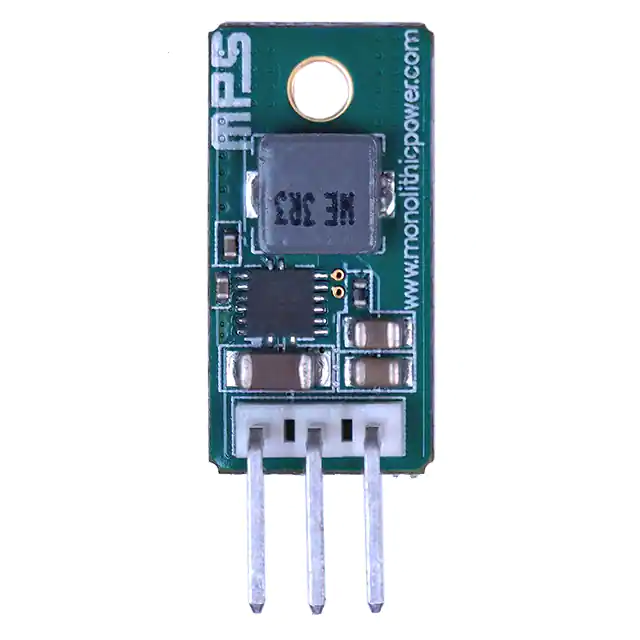
PRODUCT PACKAGE AND DIMENSIONS
Pin
Designation
Function
1
VIN
Input Voltage
2
GND
Power Ground
3
VOUT
Output Voltage
BOTTOM VIEW
TOP VIEW
NOTE:
Contact factory for different sizes of the boards (Quantity >2k).
SIDE VIEW
For more information, Gerber files, and PCB layout, please contact
mEZsupport@monolithicpower.com
mEZD71202A Rev. 1.1
www.MonolithicPower.com
3/8/2017
MPS Proprietary Information. Patent Protected. Unauthorized Photocopy and Duplication Prohibited.
Preliminary Specifications Subject to Change
© 2017 MPS. All Rights Reserved.
2
�