TM
MP1519
1x, 1.5x, 2x High Efficiency Charge Pump
4 White LED Driver
The Future of Analog IC Technology
TM
DESCRIPTION
FEATURES
The MP1519 is a fully automatic driver for
powering four white LEDs, with up to 4V
forward voltage, from a single Li-Ion or three
NiMH cells. The driver performs all of the
sensing and control to run the LEDs at an
optimum charge pump ratio for efficiency
without an expensive inductor. The driver
allows PWM operation to support brightness
control.
•
•
•
•
•
•
•
•
•
•
•
•
•
The tiny 3mm x 3mm QFN16 package and
small external capacitors allow for the most
compact white LED solution available.
EVALUATION BOARD REFERENCE
Board Number
Dimensions
EV0042
2.4”X x 1.9”Y x 0.4”Z
2% LED Current Matching
High Efficiency (>93%)
Current Source Outputs
No Ballast Resistors Required
1x, 1.5x and 2x Automatic Modes
Constant Frequency Operation
Automatic LED Detection
High and Low Frequency PWM Capability
2.5V to 5.5V Operation
Less than 1μA Leakage during Shutdown
Detects Changes in Battery Level
No External Schottky Diode Required
Soft-Start and Soft Switching Operation
APPLICATIONS
•
•
•
Cell Phones
PDA or Hand Held Computers
White LED Application at 3.6V Supply
“MPS” and “The Future of Analog IC Technology” are Trademarks of Monolithic
Power Systems, Inc.
TYPICAL APPLICATION
MP1519
BATT
ENABLE
5, 13
12
BATT
C1A
EN
C1B
Efficiency vs
Supply Voltage
4
7
100
90
GND
3, 10
RADJ
GND
C2A
C2B
LED1
LED2
8
LEDC
LED3
LED4
6
9
14
15
ILED=20mA
70
60
50
ILED=10mA
40
30
20
16
10
0
2.5
1
LED4
MP1519 Rev. 1.9
10/8/2007
ILED=5mA
80
EFFICIENCY (%)
11
VLED = 3.35V @ 20mA
LED3
LED2
LED1
3.0
3.5
4.0
SUPPLY VOLTAGE (V)
www.MonolithicPower.com
MPS Proprietary Information. Unauthorized Photocopy and Duplication Prohibited.
© 2007 MPS. All Rights Reserved.
4.5
1
�TM
MP1519 – 1X, 1.5X, 2X CHARGE PUMP 4 WHITE LED DRIVER
ABSOLUTE MAXIMUM RATINGS (1)
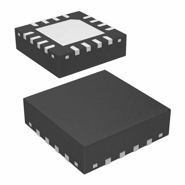
PACKAGE REFERENCE
VBATT to GND .............................................. 6.5V
Power Dissipation (QFN) ........................... 1.0W
Logic Inputs to GND ................... –0.3V to +6.5V
Storage Temperature ..............–65°C to +150°C
Junction Temperature...............................150°C
TOP VIEW
PIN 1 ID
LED3 LED2 LED1 BATT
16
15
14
13
LED4
1
12
EN
NC
2
11
RADJ
GND
3
10
GND
C1A
4
9
C2B
5
6
BATT
C2A
7
Recommended Operating Conditions
Input Voltage VBATT ...................... 2.5V to 5.5V
Operating Temperature .............–40°C to +85°C
Thermal Resistance
8
(3)
θJA
θJC
3x3 QFN16 ............................. 60 ...... 14... °C/W
C1B LEDC
EXPOSED PAD
CONNECT TO PIN 8
Part Number*
Package
Temperature
MP1519DQ
QFN16
(3mm x 3mm)
–40°C to +85°C
*
(2)
Notes:
1) Exceeding these ratings may damage the device.
2) The device is not guaranteed to function outside of its
operating conditions.
3) Measured on approximately 1” square of 1 oz copper.
For Tape & Reel, add suffix –Z (eg. MP1519DQ–Z)
For RoHS Compliant Packaging, add suffix –LF
(eg. MP1519DQ–LF–Z)
ELECTRICAL CHARACTERISTICS
VBATT = 5V, TA = +25°C, unless otherwise noted.
Parameter
Input Supply Voltage
Symbol
VBATT
VBATT at 1x to 1.5x Mode Switch
VBATT 1x-1.5x
VBATT at 1.5x to 2x Mode Switch
VBATT 1.5x-2x
VBATT at 2x to 1.5x Mode Switch
VBATT 2x-1.5x
VBATT at 1.5x to 1x Mode Switch
VBATT 1.5x-1x
Supply Current
IBATT
Supply Current Shutdown
Current Matching (4)
Enable Voltage, High
Enable Voltage, Low
Enable Pin Leakage
Charge Pump Frequency
Time to Standby Mode (5)
Enable Pin PWM Frequency Limit
LED Current
IBATT SHDN
ILED MATCH
VEN (HIGH)
VEN (LOW)
IEN
FCP
TOFF
FHPWM
ILED
Condition
Min
2.5
ILED = 20mA, VBATT Decreasing,
VLED = 3.35V @ 20mA
ILED = 20mA, VBATT Decreasing,
VLED = 3.35V @ 20mA
VBATT Increasing,
VLED = 3.35V @ 20mA
VBATT Increasing,
VLED = 3.35V @ 20mA
4 LEDs at 20mA, 2x Mode,
VBATT = 2.5V
VEN = 0V
ILED = 20mA
0.8
VEN = 5V
VBATT = 3.3V
Enable Switched Low
1.0
RSET = 1.54kΩ
18
Typ
Max
5.5
Units
V
3.6
V
2.8
V
3.1
V
3.8
V
164
180
mA
0.1
1.5
2.0
1.0
0.1
1.3
30
50
20
1
5.0
2.2
µA
%
V
V
µA
MHz
µs
KHz
mA
1
1.6
22
Notes:
4) Matching is defined as the difference of the maximum to minimum current divided by the sum of the maximum and minimum currents.
5) Standby mode switches to shutdown when the output voltage on LEDC drifts back to GND.
MP1519 Rev. 1.9
10/8/2007
www.MonolithicPower.com
MPS Proprietary Information. Unauthorized Photocopy and Duplication Prohibited.
© 2007 MPS. All Rights Reserved.
2
�TM
MP1519 – 1X, 1.5X, 2X CHARGE PUMP 4 WHITE LED DRIVER
TYPICAL PERFORMANCE CHARACTERISTICS
Voltage Ripple
in 1.5x Mode
4 x 10mA LEDs
VBATT
20mV/div.
VLEDC
20mV/div.
400ns/div.
Startup in 1.5x Mode
Startup in 1x Mode
4 x 10mA LEDs
4 x 10mA LEDs
VEN
5V/div.
VEN
5V/div.
IBATT
100mA/div.
IBATT
100mA/div.
Analog Dimming
16
Circuit of Figure 3, VBATT = 3.6V
12
LED CURRENT (mA)
LED CURRENT (mA)
14
12
10
8
6
4
2
0
MP1519 Rev. 1.9
10/8/2007
0
1
2
DC VOLTAGE (V)
3
LED Current Matching
LED4
LED3
11
10
9
LED2
LED1
8
7
6
2.5
3.0
3.5
4.0
SUPPLY VOLTAGE (V)
www.MonolithicPower.com
MPS Proprietary Information. Unauthorized Photocopy and Duplication Prohibited.
© 2007 MPS. All Rights Reserved.
4.5
3
�TM
MP1519 – 1X, 1.5X, 2X CHARGE PUMP 4 WHITE LED DRIVER
PIN FUNCTIONS
Pin #
Name Description
1
LED4
2
3, 10
NC
GND
4
C1A
5, 13
BATT
6
C2A
7
C1B
8
LEDC
9
C2B
11
RADJ
12
EN
14
LED1
15
LED2
16
LED3
MP1519 Rev. 1.9
10/8/2007
#4 LED Driver. Connect the #4 LED between LED4 and LEDC, with the anode at LED4, and
the cathode at LEDC. If the #4 LED is not used, leave LED4 unconnected.
No Connect.
Ground.
Charge Pump Capacitor #1 Positive Node. Connect the positive side of the #1 charge pump
capacitor to C1A. Typical applications require C1 to be 1μF.
Battery Power Input. Connect the 2.5V to 5.5V input source between BATT and GND. Bypass
BATT to GND with a 1μF or greater capacitor.
Charge Pump Capacitor #2 Positive Node. Connect the positive side of the #2 charge pump
capacitor to C2A. Typical applications require C2 to be 1μF.
Charge Pump Capacitor #1 Negative Node. Connect the negative side of the #1 charge pump
capacitor to C1B.
LED Common for the Cathodes. Connect the cathodes of the LEDs to LEDC and to a 4.7μF
bypass capacitor. Do not connect to any other ground, supply or pin.
Note: Exposed pad on backside is connected to this pin. Do Not Ground.
Charge Pump Capacitor #2 Negative Node. Connect the negative side of the #2 charge pump
capacitor to C2B.
LED Current Adjust Input. Connect a resistor between RADJ and GND to set the LED current.
All of the LEDs regulate at the same current. See Setting the LED Current.
Enable Input. Drive EN high to turn on the MP1519, drive EN low to shutdown the MP1519. To
use burst-mode brightness control, drive EN with a PWM signal. See Burst Mode Dimming.
#1 LED Driver. Connect the #1 LED between LED1 and LEDC, with the anode at LED1, and
the cathode at LEDC. If the #1 LED is not used, leave LED1 unconnected.
#2 LED Driver. Connect the #2 LED between LED2 and LEDC, with the anode at LED2, and
the cathode at LEDC. If the #2 LED is not used, leave LED2 unconnected.
#3 LED Driver. Connect the #3 LED between LED3 and LEDC, with the anode at LED3, and
the cathode at LEDC. If the #3 LED is not used, leave LED3 unconnected.
www.MonolithicPower.com
MPS Proprietary Information. Unauthorized Photocopy and Duplication Prohibited.
© 2007 MPS. All Rights Reserved.
4
�TM
MP1519 – 1X, 1.5X, 2X CHARGE PUMP 4 WHITE LED DRIVER
OPERATION
The MP1519 is a charge pump that drives 4
LEDs from a 2.5V to 5.5V input voltage. It
automatically switches between 1x, 1.5x and 2x
charge pump modes to optimize efficiency while
maintaining LED current regulation.
Four drivers independently regulate the current
through the LEDs, therefore matching LEDs are
not required.
BATT
BATT
5, 13
The MP1519 employs soft switching and
soft-start to prevent overloading the battery
source at turn-on and charge pump mode
switching.
While operating, the MP1519 continually
monitors the LED current and battery voltage
and automatically switches between charge
pump modes to retain LED current regulation
through all LEDs as the battery voltage
fluctuates.
FAULT
BATTERY
SENSOR
FAULT
ENABLE
EN
CURRENT
SOURCE
LED1
CURRENT
SOURCE
LED2
CURRENT
SOURCE
LED3
CURRENT
SOURCE
LED4
14
15
CONTROLLER
12
FAULT
SHUTDOWN
FAULT
16
1
LED
ENABLE
RADJ
11
ISET
CURRENT
GENERATOR
PUMP SOFT
MODE START
LED4
LED3
LED2
LED1
LEDC
8
C1A
1.25V
BANDGAP
REFERENCE
4
CHARGE PUMP
C1B
7
C2A
6
GND
3, 10
C2B
9
Figure 1—Functional Block Diagram
MP1519 Rev. 1.9
10/8/2007
www.MonolithicPower.com
MPS Proprietary Information. Unauthorized Photocopy and Duplication Prohibited.
© 2007 MPS. All Rights Reserved.
5
�TM
MP1519 – 1X, 1.5X, 2X CHARGE PUMP 4 WHITE LED DRIVER
APPLICATION INFORMATION
COMPONENT SELECTION
Startup
When power is applied to the BATT, driving EN
high will enable the MP1519. The MP1519 begins
by checking for open LEDs and determining the
optimum charge pump mode. The lowest charge
pump mode that allows the programmed LED
current in all LEDs is set. This will occur during
initial turn-on or during analog mode and burst
mode dimming.
Shutdown
Driving EN low for more than 30μs will disable
the MP1519. For safety the MP1519 runs a
small supervisory circuit in standby to protect
the charge pump output LEDC. The circuit
shuts down when the charge pump output
returns to zero volts (this can take a few
seconds). The MP1519 is in true shutdown
mode when LEDC is zero and the 30μs time
interval has passed. The supply current should
be less than 1μA.
Setting the LED Current
The LED regulation current is set through the
resistor R1 (refer to the typical application circuit
on page 1). The voltage across R1 is fixed at
1.25V, and the current through that resistor sets
the current through the LEDs.
Figure 2 shows LED Current (ILED) vs. R1 with
VBATT = 3.6V.
LED CURRENT (mA)
25
15
10
5
0
5
10
15
Figure 2—ILED vs. R1
MP1519 Rev. 1.9
10/8/2007
R1=
31.25
ILED
Where R1 is in kΩ, and ILED is in mA. Suitable
values for R1 are greater than 1.2kΩ.
Soft-Start
During startup and mode switching, an internal
soft-start prevents excessive input current,
preventing excessive loading of the battery or
input power source.
Burst Mode Dimming
To dim the part using burst mode, drive EN with a
PWM signal. Each time EN is driven high, the
MP1519 goes through the initial startup routine
and checks for open LEDs, and the charge pump
step-up mode is reset.
When EN goes low, the LED current immediately
goes to zero. After EN is held low for 30μs or
longer, and LEDC falls below GND, the MP1519
operating current drops below 1μA to improve
battery life. Maintain the frequency of the PWM
signal between 50Hz and 50KHz. Going above
50KHz the accuracy of the PWM signal will be
degraded due to the startup time, and below
50Hz, the LED flicker will be evident to the eye.
Ideally, the LED current increases proportionally
with the duty cycle of the PWM signal and is
independent of the dimming frequency.
Analog Mode Dimming
Analog dimming can be accomplished with the
circuit in Figure 3. The circuit provides 1mA to
15mA dimming with VDC = 0 to 3V. The minimum
LED current the MP1519 can regulate is
approximately 1mA.
20
0
Choose R1 for the desired LED current according
to the equation:
20
LEDC
Do not drive or force LEDC as it may be shorted
to ground or may be pumped down by the
controller in the MP1519 at any time. Excessive
capacitance on the LEDC node can cause the
internal controller to time out before the charge
pump can be ready. Missing the timeouts will
cause excessive pumping and a loss of efficiency.
The MP1519 requires C1 and C2 be of the same
value and type.
www.MonolithicPower.com
MPS Proprietary Information. Unauthorized Photocopy and Duplication Prohibited.
© 2007 MPS. All Rights Reserved.
6
�TM
MP1519 – 1X, 1.5X, 2X CHARGE PUMP 4 WHITE LED DRIVER
TYPICAL APPLICATION CIRCUITS
MP1519
BATT
ENABLE
VDC
0V to 3V
GND
5, 13
12
11
3, 10
BATT
C1A
EN
C1B
RADJ
C2A
GND
C2B
LED1
LED2
8
LEDC
LED3
LED4
4
7
6
9
14
15
16
1
LED4
LED3
LED2
LED1
Figure 3—Analog Dimming Circuit
MP1519 Rev. 1.9
10/8/2007
www.MonolithicPower.com
MPS Proprietary Information. Unauthorized Photocopy and Duplication Prohibited.
© 2007 MPS. All Rights Reserved.
7
�TM
MP1519 – 1X, 1.5X, 2X CHARGE PUMP 4 WHITE LED DRIVER
PACKAGE INFORMATION
QFN16 (3mm x 3mm)
2.90
3.10
1.50
1.80
0.30
0.50
PIN 1 ID
MARKING
0.18
0.30
2.90
3.10
PIN 1 ID
INDEX AREA
13
16
12
PIN 1 ID
SEE DETAIL A
1
1.50
1.80
0.50
BSC
4
9
5
8
TOP VIEW
BOTTOM VIEW
PIN 1 ID OPTION A
0.30x45º TYP.
PIN 1 ID OPTION B
R0.20 TYP.
0.80
1.00
0.20 REF
0.00
0.05
DETAIL A
SIDE VIEW
2.90
NOTE:
1.70
1) ALL DIMENSIONS ARE IN MILLIMETERS.
2) EXPOSED PADDLE SIZE DOES NOT INCLUDE MOLD FLASH.
3) LEAD COPLANARITY SHALL BE 0.10 MILLIMETER MAX.
4) DRAWING CONFORMS TO JEDEC MO-220, VARIATION VEED-4.
5) DRAWING IS NOT TO SCALE.
0.70
0.25
0.50
RECOMMENDED LAND PATTERN
NOTICE: The information in this document is subject to change without notice. Users should warrant and guarantee that third
party Intellectual Property rights are not infringed upon when integrating MPS products into any application. MPS will not
assume any legal responsibility for any said applications.
MP1519 Rev. 1.9
10/8/2007
www.MonolithicPower.com
MPS Proprietary Information. Unauthorized Photocopy and Duplication Prohibited.
© 2007 MPS. All Rights Reserved.
8
�