MP1906
80V, Half-Bridge, Gate Driver
The Future of Analog IC Technology
DESCRIPTION
FEATURES
The MP1906 is a high-performance, 80V, gate
driver that can drive two external N-MOSFETs
in a half-bridge configuration with a 12V gate
supply. It accepts independent gate input
signals and provides shoot-through prevention.
During under-voltage lockout, the output of the
high- and low-side drivers goes low to prevent
erratic operation under low supply conditions.
The high-current driving capability and short dead
time make it suitable for high-power and highefficiency power applications, such as telecom
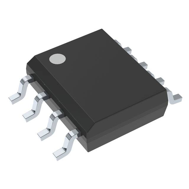
DC-DC converters. The compact 8-pin SOIC
package minimizes the component count and
the board space.
Drives Two Low-Cost, High-Efficiency NMOSFETs
10V-16V Gate Drive Supply
3.3V, 5V Logic Compatibility
80ns Propagation Delay
Less than 90μA Quiescent Current
Under-Voltage Lockout for Both Channels
Input-Signal-Overlap Protection
Internal 150ns Dead Time
Available in a Compact 8-pin SOIC Package
APPLICATIONS
Motor Drivers
Half-Bridge Power Supplies
Avionics DC-DC Converters
Active-Clamp Forward Converters
All MPS parts are lead-free and adhere to the RoHS directive. For MPS green
status, please visit MPS website under Products, Quality Assurance page.
“MPS” and “The Future of Analog IC Technology” are registered trademarks of
Monolithic Power Systems, Inc.
TYPICAL APPLICATION
VIN=12V
Up to 80V
VCC
BT
HPWM
TG
CONTROLLER
LPWM
SW
GND
To Output
Load
BG
MP1906 Rev. 1.0
www.MonolithicPower.com
1/3/2013
MPS Proprietary Information. Patent Protected. Unauthorized Photocopy and Duplication Prohibited.
© 2013 MPS. All Rights Reserved.
1
�MP1906—80V, HALF-BRIDGE, GATE DRIVER
ORDERING INFORMATION
Part Number*
Package
SOIC8
MP1906DS
Top Marking
MP1906
*For Tape & Reel, add suffix –Z (e.g. MP1906DS–Z).
For RoHS compliant packaging, add suffix –LF (e.g. MP1906DS–LF–Z)
PACKAGE REFERENCE
TOP VIEW
VCC
1
8
BT
HPWM
2
7
TG
LPWM
3
6
SW
GND
4
5
BG
ABSOLUTE MAXIMUM RATINGS
(1)
Input Voltage VCC ..........................-0.3V to +18V
Voltage on SW VSW .............................................
-0.3V (-5V < 10ns) to +100V
Voltage on BT VBT .............................. VSW +18V
Logic Inputs ........................................................
-0.3 to (VCC+6.5V), or 18.5V for VCC ≥ 12V
Continuous Power Dissipation (TA = 25°C) (2)
………………………………………………...1.4W
Junction Temperature .............. -40°C to +150°C
Lead Temperature (Solder 10sec) ............260°C
Storage Temperature ............... -55°C to +150°C
Recommended Operating Conditions
(3)
Thermal Resistance
(4)
θJA
θJC
SOIC8 ..................................... 90 ...... 45... °C/W
Notes:
1) Exceeding these ratings may damage the device.
2) The maximum allowable power dissipation is a function of the
maximum junction temperature TJ (MAX), the junction-toambient thermal resistance θJA, and the ambient temperature
TA. The maximum allowable continuous power dissipation at
any ambient temperature is calculated by PD (MAX) = (TJ
(MAX)-TA)/θJA. Exceeding the maximum allowable power
dissipation will cause excessive die temperature, and the
regulator will go into thermal shutdown. Internal thermal
shutdown circuitry protects the device from permanent
damage.
3) The device is not guaranteed to function outside of its
operating conditions.
4) Measured on JESD51-7, 4-layer PCB.
Input Voltage VCC .............................. 10V to 16V
Maximum Voltage on SW VSW ..................... 80V
Logic Inputs .........................................0V to VCC
Voltage slew rate on SW...................... < 50V/ns
PWM frequency .................................. < 300kHz
Operating Junction Temp. (TJ) . -40°C to 125°C
MP1906 Rev. 1.0
www.MonolithicPower.com
1/3/2013
MPS Proprietary Information. Patent Protected. Unauthorized Photocopy and Duplication Prohibited.
© 2013 MPS. All Rights Reserved.
2
�MP1906—80V, HALF-BRIDGE, GATE DRIVER
ELECTRICAL CHARACTERISTICS
VCC = 12V, VSW=0V, no load on TG or BG, TA = 25°C, unless otherwise noted.
Parameter
Supply Current
VCC quiescent current
VCC operation current
Bootstrap quiescent current
Bootstrap operation current
SW BT leakage current
Input
LPWM falling threshold
LPWM rising threshold
HPWM falling threshold
HPWM rising threshold
Under-Voltage Protection (UVLO)
VCC rising threshold
VCC threshold hysteresis
Bootstrap rising threshold
Bootstrap threshold hysteresis
Gate Driver Output
Low-side gate pull-up peak
current (5)
Low-side gate pull-down peak
current (5)
High-side gate pull-up peak
current (5)
Symbol Condition
ICCQ
ICC
IBTQ
IBT
ILK
VLPWM=5V, VHPWM= 0V
f=50kHz, CLOAD BG=1nF
VLPWM=5V, VHPWM= 0V
f=50kHz, CLOAD TG=1nF
VSW=VBT=80V
VLPWMF
VLPWMR
VHPWMF
VHPWMR
Min
Typ
Max
Units
70
90
0.9
30
0.7
0.1
110
1.5
μA
mA
μA
mA
μA
1
0.5
0.8
2.5
0.8
2.5
VCCTHR
VCCTHH
VBTTHR
VBTTHH
8.2
4.5
8.8
0.7
5.5
0.65
9.4
6.5
V
V
V
V
V
V
V
V
IBGU
VBG=0V
350
mA
IBGD
VBG=12V
1
A
ITGU
VTG=0V
350
mA
High-side gate pull-down peak
VTG=12V
1
A
ITGD
current (5)
Propagation Delays, Dead Times and Output Rising and Falling Times (CLoad=1nF cap) (please see timing
diagram)
Turn-on propagation delay (TG)
τON TG VSW=0V
80
150
ns
τ
Turn-off propagation delay (TG)
80
150
ns
VSW=0V
OFF TG
Turn-on rise time (TG)
τRISE TG
50
100
ns
Turn-off fall time (TG)
τFALL
Turn-on propagation delay (BG)
τON
Turn-off propagation delay (BG)
τOFF BG
τRISE_BG
80
150
ns
50
100
ns
τFALL_BG
30
100
ns
τDT
150
250
ns
Turn-on rise time (BG)
Turn-off fall time (BG)
Deadtime, LS turn-off to HS turnon & HS turn-on to LS turn-off
TG
BG
30
100
ns
80
150
ns
MP1906 Rev. 1.0
www.MonolithicPower.com
1/3/2013
MPS Proprietary Information. Patent Protected. Unauthorized Photocopy and Duplication Prohibited.
© 2013 MPS. All Rights Reserved.
3
�MP1906—80V, HALF-BRIDGE, GATE DRIVER
ELECTRICAL CHARACTERISTICS(CONTIUUED)
VCC = 12V, VSW=0V, no load on TG or BG, TA = 25°C, unless otherwise noted.
Parameter
Symbol
Condition
Min
Typ
Max
Units
ILPWM
IHPWM
ILPWM=5V
IHPWM=5V
-8
1
-3
3
-1
8
μA
μA
VBGL
VBGH
VTGL
VTGH
IBG=100mA
IBG=-100mA, VBGH=VCC-VBG
ITG=100mA
ITG=-100mA, VTGH=VCC-VTG
0.4
1.5
0.4
1.5
0.7
1.7
0.7
1.7
V
V
V
V
50
ns
LPWM source current
HPWM sink current
Floating Gate Driver
BG-output-low to GND
BG-output-high to rail
TG-output-low to SW
TG-output-high to rail
Switching Specifications
Minimum input pulse width to
change the output(5)
τPWM_min
Notes:
5) Guaranteed by design
LPWM
ton
tr
toff
tf
BG
HPWM
ton
tr
toff
tf
TG
Figure 1: Gate Driver Timing Diagram
MP1906 Rev. 1.0
www.MonolithicPower.com
1/3/2013
MPS Proprietary Information. Patent Protected. Unauthorized Photocopy and Duplication Prohibited.
© 2013 MPS. All Rights Reserved.
4
�MP1906—80V, HALF-BRIDGE, GATE DRIVER
TYPICAL CHARACTERISTICS
VDD=12V, VSW=0V, TA=+25°C, unless otherwise noted.
Low Level Output Voltage
vs. Temperature
0.8
10
1.75
0.7
9
1.5
0.6
VTGH
1.0
VBGH
0.75
0.5
8
VCCTH,VBTTHR(V)
1.25
0.25
0.5
0.4
VTGL
0.3
VBGL
0.2
7
0
50
100
5
4
3
2
0
50
100
0
-50
150
0.9
155
9
0.8
135
VCCTHH,VBTTHH(V)
7
VCCTHF
6
5
4
3
VBTTHF
2
1
0.7
0.6
0.5
0.4
VBTTHH
VCCTHH
0.3
0.2
0.1
0
-50
120
Undervoltage Lockout
Hysteresis vs. Temperature
0
50
100
150
0
-50
0
50
100
150
0
50
100
150
Propagation Delay vs.
Temperature
TON_TG,TOFF_TG,TON_BG,
TOFF_BG(nS)
Undervoltage Lockout
Threshold vs. Temperature
(Falling)
10
8
VBTTHR
1
0
-50
150
VCCTHR
6
0.1
0
-50
VCCTHF,VBTTHF(V)
Undervoltage Lockout
Threshold vs. Temperature
(Rising)
2
VTGL,VBGL(V)
VTGH,VBGH(V)
High Level Output
Voltage vs. Temperature
115
TON_BG
TON_TG
95
75
55
35
TOFF_TG
TOFF_BG
15
-5
-25
-50
0
50
100
150
Quiescent Current
vs. Temperature
100
80
ICCQ
60
40
IBTQ
20
0
-50
0
50
100
150
MP1906 Rev. 1.0
www.MonolithicPower.com
1/3/2013
MPS Proprietary Information. Patent Protected. Unauthorized Photocopy and Duplication Prohibited.
© 2013 MPS. All Rights Reserved.
5
�MP1906—80V, HALF-BRIDGE, GATE DRIVER
TYPICAL PERFORMANCE CHARACTERISTICS
VCC = 12V, VSW=0V, 1nF load on TG and BG, TA = 25°C, unless otherwise noted.
Turn-on Propagation
Delay
VHPWM
2V/div.
VTG
5V/div.
Turn-on Propagation
Delay
VLPWM
2V/div.
VHPWM
2V/div.
VBG
5V/div.
VTG
5V/div.
Turn-off Propagation
Delay
VLPWM
2V/div.
Turn-off Propagation
Delay
Drive Rise Time(1nF Load)
Drive Rise Time(1nF Load)
VBG
5V/div.
VTG
5V/div.
VBG
5V/div.
Drive Fall Time(1nF Load)
Drive Fall Time(1nF Load)
Input Signal Overlap
Protection
VHPWM
5V/div.
VLPWM
5V/div.
VTG
5V/div.
VBG
5V/div.
VTG
5V/div.
VBG
10V/div.
MP1906 Rev. 1.0
www.MonolithicPower.com
1/3/2013
MPS Proprietary Information. Patent Protected. Unauthorized Photocopy and Duplication Prohibited.
© 2013 MPS. All Rights Reserved.
6
�MP1906—80V, HALF-BRIDGE, GATE DRIVER
PIN FUNCTIONS
Pin #
Name
Description
Supply Input. Supplies power to all internal circuitry. Requires a decoupling capacitor
to ground placed close to this pin to ensure a stable and clean supply.
Logic input for high-side gate driver output.
Logic input for low-side gate driver output. Active low.
Ground.
1
VCC
2
3
4
HPWM
LPWM
GND
5
BG
Gate Driver Output for low-side MOSFET.
6
SW
Source Return for high-side MOSFET.
7
TG
Gate Driver Output for high-side MOSFET.
8
BT
Bootstrap. Internal power supply pin for high-side floating driver. Add a 1µF ceramic
bootstrap capacitor from BT to SW pin.
MP1906 Rev. 1.0
www.MonolithicPower.com
1/3/2013
MPS Proprietary Information. Patent Protected. Unauthorized Photocopy and Duplication Prohibited.
© 2013 MPS. All Rights Reserved.
7
�MP1906—80V, HALF-BRIDGE, GATE DRIVER
FUNCTIONAL BLOCK DIAGRAM
VCC
UVLO
RDY
Turn-on
Delay
HPWM
TG
Driver
Level Shift
Dead Time
Control
SW
Shoot
Through
Prevention
LPWM
BT
UVLO
VCC
RDY
Turn-on
Delay
Driver
BG
GND
Figure 2: Functional Block Diagram
MP1906 Rev. 1.0
www.MonolithicPower.com
1/3/2013
MPS Proprietary Information. Patent Protected. Unauthorized Photocopy and Duplication Prohibited.
© 2013 MPS. All Rights Reserved.
8
�MP1906—80V, HALF-BRIDGE, GATE DRIVER
OPERATION
Switch Shoot-through Protection
The input signals of HPWM and LPWM are
independently controlled. Input shoot-through
protection circuitry prevents shoot-through
between the TG and BG outputs. Only one of
the FET drivers can be on at one time. If HPWM
is high and LPWM is low, both TG and BG are
OFF.
Under Voltage Lockout
When VCC or VBT goes below their respective
UVLO threshold, both BG and TG outputs will go
low to both FETS. Once VCC and VBT rises above
the UVLO threshold, both TG and BG will stay
low until there is a rising edge on either HPWM
or LPWM.
Figure 3 shows the operation of the TG and BG
under different HPWM and LPWM and UVLO
conditions.
HPWM
LPWM
TG
BG
Figure 3: Input/Output Timing Diagram
MP1906 Rev. 1.0
www.MonolithicPower.com
1/3/2013
MPS Proprietary Information. Patent Protected. Unauthorized Photocopy and Duplication Prohibited.
© 2013 MPS. All Rights Reserved.
9
�MP1906—80V, HALF-BRIDGE, GATE DRIVER
APPLICATION INFORMATION
Reference Design Circuits
Half Bridge Motor Driver
In a half-bridge converter topology, the MOSFETdriving signals have a dead time: HPWM and
LPWM driven with alternating signals from the
PWM controller. The input voltage can be up to
80V in this application.
Up to 80V
Vin=12V
GND
+
VCC
A
GND
HPWM
HPWM
LPWM
LPWM
BT
TG
SW
GND
BG
MP1906
GND
GND
Figure 4: Half-Bridge Motor Driver
Active-Clamp-Forward Converter
An
active-clamp-forward-converter
topology
alternately drives the MOSFETs. The high-side
MOSFET and the capacitor, CRESET, reset the
power transformer in a lossless manner. This
topology runs well at duty cycles exceeding 50%.
However, the input voltage may not run at 80V.
Up to 80V
Vin=12V
1 2
GND
Secondary
VCC
Circuit
GND
HPWM
HPWM
LPWM
LPWM
3
4
BT
Creset
TG
SW
GND
BG
MP1906
GND
GND
Figure 5: Active-Clamp Forward Converter
MP1906 Rev. 1.0
www.MonolithicPower.com
1/3/2013
MPS Proprietary Information. Patent Protected. Unauthorized Photocopy and Duplication Prohibited.
© 2013 MPS. All Rights Reserved.
10
�MP1906– 80V HALF BRIDGE GATE DRIVER
PACKAGE INFORMATION
SOIC8
0.189(4.80)
0.197(5.00)
8
0.050(1.27)
0.024(0.61)
5
0.063(1.60)
0.150(3.80)
0.157(4.00)
PIN 1 ID
1
0.228(5.80)
0.244(6.20)
0.213(5.40)
4
TOP VIEW
RECOMMENDED LAND PATTERN
0.053(1.35)
0.069(1.75)
SEATING PLANE
0.004(0.10)
0.010(0.25)
0.013(0.33)
0.020(0.51)
0.0075(0.19)
0.0098(0.25)
SEE DETAIL "A"
0.050(1.27)
BSC
SIDE VIEW
FRONT VIEW
0.010(0.25)
x 45o
0.020(0.50)
GAUGE PLANE
0.010(0.25) BSC
0o-8o
0.016(0.41)
0.050(1.27)
DETAIL "A"
NOTE:
1) CONTROL DIMENSION IS IN INCHES. DIMENSION IN
BRACKET IS IN MILLIMETERS.
2) PACKAGE LENGTH DOES NOT INCLUDE MOLD FLASH,
PROTRUSIONS OR GATE BURRS.
3) PACKAGE WIDTH DOES NOT INCLUDE INTERLEAD FLASH
OR PROTRUSIONS.
4) LEAD COPLANARITY (BOTTOM OF LEADS AFTER FORMING)
SHALL BE 0.004" INCHES MAX.
5) DRAWING CONFORMS TO JEDEC MS-012, VARIATION AA.
6) DRAWING IS NOT TO SCALE.
NOTICE: The information in this document is subject to change without notice. Users should warrant and guarantee that third
party Intellectual Property rights are not infringed upon when integrating MPS products into any application. MPS will not
assume any legal responsibility for any said applications.
MP1906 Rev. 1.0
www.MonolithicPower.com
1/3/2013
MPS Proprietary Information. Patent Protected. Unauthorized Photocopy and Duplication Prohibited.
© 2013 MPS. All Rights Reserved.
11
�