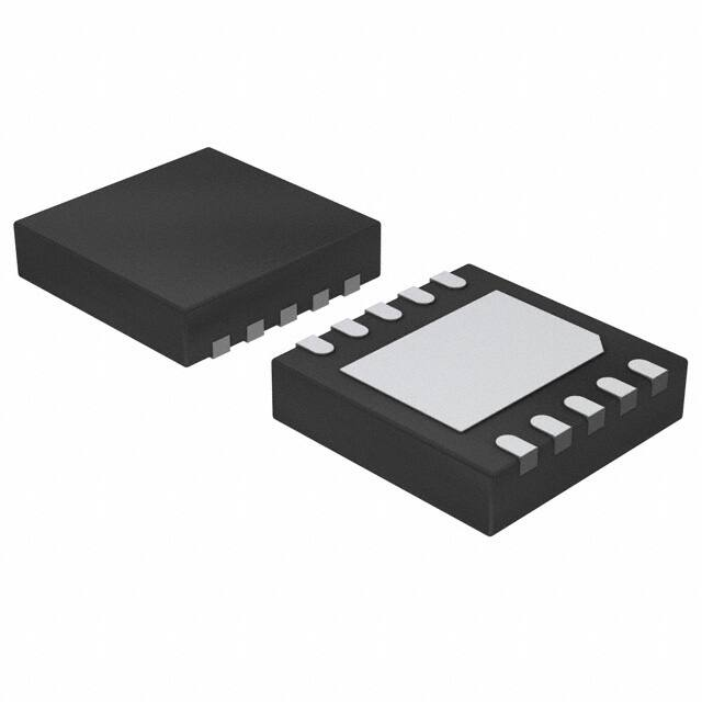
MP1924A
100V, 4A, High Frequency
Half-Bridge Gate Driver
The Future of Analog IC Technology
DESCRIPTION
FEATURES
The MP1924A is a high-frequency, half-bridge,
N-channel power MOSFET driver. Its low-side
and high-side driver channels are controlled
independently and matched with less than 5ns
of time delay. Under-voltage lockout (UVLO) on
both the high-side and low-side supplies forces
the outputs low in the event that the supply is
insufficient. The integrated bootstrap diode
reduces the external component count.
The MP1924A is available in QFN-10
(4mmx4mm) and SOIC-8 packages.
Drives an N-Channel MOSFET Half-Bridge
115V Bootstrap Voltage Range
On-Chip Bootstrap Diode
Typical Propagation Delay of 20ns
Gate Driver Matching of Less than 5ns
Drives a 2.2nF Load with 15ns of Rise Time
and 12ns of Fall Time at 12V VDD
TTL-Compatible Input
Quiescent Current of Less than 150µA
UVLO for Both High-Side and Low-Side
Gate Drivers
QFN-10 (4mmx4mm) and SOIC-8
Packages
APPLICATIONS
Motor Drivers
Telecom Half-Bridge Power Supplies
Avionics DC/DC Converters
Two-Switch Forward Converters
Active Clamp Forward Converters
All MPS parts are lead-free, halogen free, and adhere to the RoHS directive. For
MPS green status, please visit the MPS website under Quality Assurance.
“MPS” and “The Future of Analog IC Technology” are registered trademarks of
Monolithic Power Systems, Inc.
TYPICAL APPLICATION
12V
VDC
VDD
INH
VDD
BST
BST
DRVH
DRVH
INH
SW
M
SW
INL
INL
DRVL
DRVL
MOTOR
DRIVER
VSS
VSS
MP1924A Rev. 1.1
www.MonolithicPower.com
2/8/2018
MPS Proprietary Information. Patent Protected. Unauthorized Photocopy and Duplication Prohibited.
© 2018 MPS. All Rights Reserved.
1
�MP1924A―100V, 4A HIGH FREQUENCY HALF-BRIDGE GATE DRIVER
ORDERING INFORMATION
Part Number
MP1924AHR*
MP1924AHS**
Package
QFN-10 (4mmx4mm)
SOIC-8
Top Marking
See Below
See Below
* For Tape & Reel, add suffix –Z (e.g. MP1924AHR–Z)
For RoHS compliant packaging, add suffix –LF (e.g. MP1924AHR–LF–Z)
** For Tape & Reel, add suffix –Z (e.g. MP1924AHS–Z)
For RoHS compliant packaging, add suffix –LF (e.g. MP1924AHS–LF–Z)
TOP MARKING (MP1924AHR)
MPS: MPS prefix
Y: Year code
WW: Week code
M1924A: Product code of MP1924AHR
LLLLLL: Lot number
TOP MARKING (MP1924AHS)
MP1924A: Part number
LLLLLLLL: Lot number
MPS: MPS prefix
Y: Year code
WW: Week code
MP1924A Rev. 1.1
www.MonolithicPower.com
2/8/2018
MPS Proprietary Information. Patent Protected. Unauthorized Photocopy and Duplication Prohibited.
© 2018 MPS. All Rights Reserved.
2
�MP1924A―100V, 4A HIGH FREQUENCY HALF-BRIDGE GATE DRIVER
PACKAGE REFERENCE
TOP VIEW
VDD 1
10
DRVL
BST
2
9
DRVH
3
8
INL
SW
4
7
INH
NC
5
6
NC
VSS
TOP VIEW
VDD
1
8
DRVL
BST
2
7
VSS
DRVH
3
6
INL
SW
4
5
INH
EXPOSED PAD
ON BACKSIDE
QFN-10 (4mmx4mm)
SOIC-8
ABSOLUTE MAXIMUM RATINGS (1)
Thermal Resistance
Supply voltage (VDD) ....................... -0.3V to 18V
SW voltage (VSW) .......................... -5.0V to 105V
BST voltage (VBST) ........................ -0.3V to 115V
BST to SW ...................................... -0.3V to 18V
DRVH to SW ........... -0.3V to (BST - SW) + 0.3V
DRVL to VSS .................... -0.3V to (VDD + 0.3V)
All other pins ...................... -0.3V to (VDD + 0.3V)
(2)
Continuous power dissipation (TA = 25°C)
QFN-10 (4mmx4mm) ............................... 2.66W
SOIC-8 ....................................................... 1.3W
Junction temperature ................................150°C
Lead temperature .....................................260°C
Storage temperature .................. -65°C to 150°C
QFN-10 (4mmx4mm) .............. 47 ....... 7.... °C/W
SOIC-8 .................................... 96 ...... 45... °C/W
Recommended Operating Conditions
(3)
(4)
θJA
θJC
NOTES:
1) Exceeding these ratings may damage the device.
2) The maximum allowable power dissipation is a function of the
maximum junction temperature TJ (MAX), the junction-toambient thermal resistance θJA, and the ambient temperature
TA. The maximum allowable continuous power dissipation at
any ambient temperature is calculated by PD (MAX) =
(TJ(MAX)-TA)/θJA. Exceeding the maximum allowable power
dissipation produces an excessive die temperature, causing
the regulator to go into thermal shutdown. Internal thermal
shutdown circuitry protects the device from permanent
damage.
3) The device is not guaranteed to function outside of its
operating conditions.
4) Measured on JESD51-7, 4-layer PCB.
Supply voltage (VDD) ..................... 8.0V to 15.0V
SW voltage (VSW) .......................... -1.0V to 100V
SW slew rate .........................................
很抱歉,暂时无法提供与“MP1924AHR-LF-Z”相匹配的价格&库存,您可以联系我们找货
免费人工找货- 国内价格
- 1+19.46538
- 50+17.69764
- 100+15.66076
