MP20041
Dual, Ultra Low Noise, High PSRR
300mA Linear Regulator
The Future of Analog IC Technology
DESCRIPTION
FEATURES
The MP20041 is a dual-channel, micropower,
ultra low noise, low dropout and high PSRR
linear regulator. The output voltage of MP20041
ranges from 1.2V to 3.6V in 100mV increments
and 1% accuracy by operating from a +2.5V to
+6.0V input. The MP20041 can supply up to
300mA of load current at each channel.
The MP20041 uses an internal PMOS as the
pass element, which consumes 114μA supply
current (both LDOs on) at no load condition.
The EN1 and EN2 pins control each output
respectively. When both channels shutdown
simultaneously, the chip will be turned off and
consume nearly zero operation current which is
suitable for battery-power devices. The
MP20041 features current limit and over
temperature protection.
Wide Operating Voltage Ranges: 2.5V to 6V
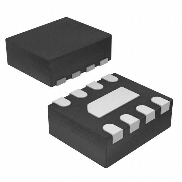
Two LDOs in a 2mmx2mm TQFN8 Package
Up to 300mA Output Current (Per Channel)
Dual Enable Pins Control Each Output
72dB PSRR at 10kHz
11μVRMS Ultra Low Noise Output with No
Noise Bypass Capacitor Required
73mV Dropout at 100mA Load
Very Fast Line/Load Transient Responses
with Small Input/Output Capacitor
Current Limit and Thermal Protection
APPLICATIONS
It is available in a 2mm x 2mm TQFN8 package.
Cellular Phones
Battery-powered Equipment
Laptop, Notebook, and Palmtop Computers
Hand-held Equipment
Wireless LAN
All MPS parts are lead-free, halogen free, and adhere to the RoHS directive. For
MPS green status, please visit MPS website under Quality Assurance. “MPS”
and “The Future of Analog IC Technology” are Registered Trademarks of
Monolithic Power Systems, Inc.
TYPICAL APPLICATION
IN
OUT1
OUT1
IN
CIN
COUT1
MP20041
EN1
EN1
EN2
EN2
OUT2
OUT2
COUT2
GND
MP20041 Rev. 1.2
7/15/2019
www.MonolithicPower.com
MPS Proprietary Information. Patent Protected. Unauthorized Photocopy and Duplication Prohibited.
© 2019 MPS. All Rights Reserved.
1
�MP20041-DUAL, ULTRA LOW NOISE, HIGH PSRR, 300mA LINEAR REGULATOR
ORDERING INFORMATION*
Part Number
VOUT1
VOUT2
Package
MP20041DGT-GJ-LF-Z
MP20041DGT-MG-LF-Z
MP20041DGT-SS-LF-Z
MP20041DGT-PP-LF-Z
1.8V
2.8V
3.3V
3.0V
2.5V
1.8V
3.3V
3.0V
TQFN8
(2mmx2mm)
Free Air Temperature (TA)
Top Marking
-40°C to +85°C
5H
7K
9P
6P
* Other output voltage versions between 1.2V and 3.3V are available in 100mV increments. Contact factory for availability.
ORDERING GUIDE**
4
** For RoHS Compliant Packaging, add suffix - LF (e.g. MP20041DGTLF-Z).
-LF); For Tape and Reel, add suffix -Z (e.g. MP20041DGT-
-
OUTPUT VOLTAGE SELECTOR GUIDE***
Code
VOUT
Code
VOUT
C
B
F
W
G
D
Y
H
E
J
K
1.2
1.3
1.5
1.6
1.8
1.85
1.9
2.0
2.1
2.5
2.6
T
L
M
N
V
P
Q
X
R
S
Z
2.65
2.7
2.8
2.85
2.9
3.0
3.1
3.15
3.2
3.3
5.0
*** Code in Bold are standard versions. For other output
voltages between 1.2V and 5.0V contact factory for availability.
Minimum order quantity on non-standard versions is 25,000
units.
MP20041 Rev. 1.2
7/15/2019
www.MonolithicPower.com
MPS Proprietary Information. Patent Protected. Unauthorized Photocopy and Duplication Prohibited.
© 2019 MPS. All Rights Reserved.
2
�MP20041-DUAL, ULTRA LOW NOISE, HIGH PSRR, 300mA LINEAR REGULATOR
PACKAGE REFERENCE
TOP VIEW
IN
1
8
OUT1
EN1
2
7
OUT2
EN2
3
6
NC
NC
4
5
GND
ABSOLUTE MAXIMUM RATINGS (1)
Supply Input Voltage .................................. 6.5V
Continuous Power Dissipation (TA = +25°C) (2)
............................................................. 1.25W
Operation Temperature Range .... -40°C to 85°C
Storage Temperature Range ...... -65°C to 150°C
Lead Temperature (Soldering, 10sec) ..... 260°C
Recommended Operating Conditions (3)
Supply Input Voltage ....................... 2.5V to 6.0V
Enable Input Voltage ......................... 0V to 6.0V
Operating Junct. Temp (TJ) ..... –40C to +125C
MP20041 Rev. 1.2
7/15/2019
Thermal Resistance (4)
θJA
θJC
2mmx2mm TQFN8……………80……16. .. C/W
Notes:
1) Exceeding these ratings may cause permanent damage to
the device.
2) The maximum allowable power dissipation is a function of the
maximum junction temperature TJ(MAX), the junction-toambient thermal resistance θJA, and the ambient temperature
TA. The maximum allowable continuous power dissipation at
any ambient temperature is calculated by PD(MAX)=(TJ(MAX)TA)/ θJA. Exceeding the maximum allowable power dissipation
will cause excessive die temperature, and the regulator will go
into thermal shutdown. Internal thermal shutdown circuitry
protects the device from permanent damage.
3) The device is not guaranteed to function outside its operating
conditions.
4) Measured on JESD51-7 4-layer board.
www.MonolithicPower.com
MPS Proprietary Information. Patent Protected. Unauthorized Photocopy and Duplication Prohibited.
© 2019 MPS. All Rights Reserved.
3
�MP20041-DUAL, ULTRA LOW NOISE, HIGH PSRR, 300mA LINEAR REGULATOR
ELECTRICAL CHARACTERISTICS
VIN=3.5V, VOUT1=1.8V, VOUT2=2.5V, CIN=COUT1=COUT2=1μF, EN1=EN2=VIN, Typical Value at TA=25C
for each LDO unless otherwise noted.
Parameter
Symbol
Input Voltage
VIN
Output Voltage Range
Condition
Min
VIN=2.5V to 6.0V
VOUT
Load regulation(5)
∆VOUT
Line Regulation(6)
∆VLINE
Maximum Output Current
Current Limit
Quiescent Current
IMAX
ILIM
IG
VDROP1
Dropout Voltage (7)
VDROP2
EN Input High Threshold
EN Input Low Threshold
EN Input Bias Current
Shutdown Supply Current
Thermal Shutdown Temperature
Thermal Shutdown Hysteresis
VIH
VIL
ISD
IGSD
TSD
∆TSD
Output Voltage Noise
Output Voltage AC PSRR
PSRR
ILOAD = 1mA to 300mA
VIN =(VOUT+0.3V or 2.5V)
to 6V, IOUT=1mA
Continuous
Short circuit current limit
No Load
VOUT1=1.8V, IOUT1 = 100mA
VOUT1=1.8V, IOUT1 = 300mA
VOUT2=2.5V, IOUT2 = 100mA
VOUT2=2.5V, IOUT2 = 300mA
VIN = 2.5V to 6.0V
VIN = 2.5V to 6.0V
EN = GND or VIN
EN1 = EN2 = GND
100Hz to 100kHz,
COUT=1μF, ILOAD=10mA
100Hz to 100kHz,
COUT=1μF, ILOAD=100mA
f=100Hz
f=1kHz
ILoad=10mA
f=10kHz
f=100Hz
f=1kHz
ILoad=150mA
f=10kHz
Max
Units
2.5
6
V
1.2
3.6
V
5
mV
0.05
%/V
-35
Typ
-10
300
525
114
75
220
60
180
1.6
0.03
140
10
0.45
300
1
mA
mA
uA
mV
mV
mV
mV
V
V
nA
uA
°C
°C
11
μVRMS
11
μVRMS
68
66
65
69
65
72
dB
dB
dB
dB
dB
dB
Notes:
5) Load Regulation= VOUT IOUT(MAX ) VOUT IOUT (MIN)
VOUT NOM
6) Line Regulation=
VOUT V
IN(MAX )
100(%)
VOUT V
IN( MIN)
V
VIN(MIN) VOUT(NOM)
INMAX
100(% / V)
7) Dropout Voltage is defined as the input to output differential when the output voltage drops 100mV below its nominal value.
MP20041 Rev. 1.2
7/15/2019
www.MonolithicPower.com
MPS Proprietary Information. Patent Protected. Unauthorized Photocopy and Duplication Prohibited.
© 2019 MPS. All Rights Reserved.
4
�MP20041-DUAL, ULTRA LOW NOISE, HIGH PSRR, 300mA LINEAR REGULATOR
PIN FUNCTIONS
Pin #
Name
Description
1
2
3
4, 6
5
7
8
IN
EN1
EN2
NC
GND
OUT2
OUT1
Supply Input Pin.
Channel 1 Enable (Active High). Do Not Float This Pin.
Channel 2 Enable (Active High). Do Not Float This Pin.
MP20041 Rev. 1.2
7/15/2019
Common Ground.
Channel 2 Output Voltage.
Channel 1 Output Voltage.
www.MonolithicPower.com
MPS Proprietary Information. Patent Protected. Unauthorized Photocopy and Duplication Prohibited.
© 2019 MPS. All Rights Reserved.
5
�MP20041-DUAL, ULTRA LOW NOISE, HIGH PSRR, 300mA LINEAR REGULATOR
TYPICAL PERFORMANCE CHARACTERISTICS
VIN=3.5V, VOUT1=1.8V, VOUT2=2.5V, IOUT1=IOUT2=0mA, CIN=COUT1=COUT2=1μF, EN1=EN2=VIN, Typical
Value at TA = 25C for Both Channel Enabled.
Quiescent Current vs.
Supply Voltage
120
90
60
30
0
2.5
3
3.5
4
4.5
5
5.5
6
Dropout Voltage vs.
Temperature
300
200
180
160
DROPOUT VOLTAGE (mV)
150
QUIESCENT CURRENT (uA)
QUIESCENT CURRENT (uA)
180
Quiescent Current vs.
Temperature
140
120
100
80
60
40
20
0
-50 -30 -10 10
30
50
70
250
VOUT1 dropout
200
150
VOUT2 dropout
100
50
0
-50 -30 -10 10
90
30
50
70
90
0.25
0.20
IO=300mA
0.15
0.10
0.05
0
-0.05
IO=0mA
-0.10
-0.15
-0.20
-0.25
-50 -30 -10 10
30
50
70
90
Out2 Voltage Accuracy vs.
Temperature
0.25
0.20
IO=300mA
0.15
0.10
0.05
0
-0.05
-0.10
-0.15
IO=0mA
-0.20
-0.25
-50 -30 -10 10
30
50
70
90
Out Voltage Accuracy vs.
Output Current
OUT VOLTAGE ACCURACY (%)
Out1 Voltage Accuracy vs.
Temperature
OUT VOLTAGE ACCURACY (%)
OUT VOLTAGE ACCURACY (%)
VIN(V)
OUTPUT CURRENT(mA)
Power Supply Rejection
Ratio vs. Frequency
120
80
100
70
60
40
0
102
50
ILOAD=10mA
MP20041 Rev. 1.2
7/15/2019
VEN
2V/div
VOUT2
ILOAD=100mA
30
VOUT
1V/div
10
103
104
105
106
FREQUENCY(Hz)
VIN=3.5V, IOUT1=IOUT2=50mA
40
20
20
EN Start Up Waveform
ILOAD=50mA
60
80
PSRR(dB)
CHANNEL ISOLATION (dB)
Channel-to-Channel
Isolation vs. Frequency
0
10
102 103 104 105 106
FREQUENCY(Hz)
VOUT1
10us/div
www.MonolithicPower.com
MPS Proprietary Information. Patent Protected. Unauthorized Photocopy and Duplication Prohibited.
© 2019 MPS. All Rights Reserved.
6
�MP20041-DUAL, ULTRA LOW NOISE, HIGH PSRR, 300mA LINEAR REGULATOR
TYPICAL PERFORMANCE CHARACTERISTICS (continued)
VIN=3.5V, VOUT1=1.8V, VOUT2=2.5V, IOUT1=IOUT2=0mA, CIN=COUT1=COUT2=1μF, EN1=EN2=VIN, Typical
Value at TA = 25C for Both Channel Enabled.
EN Shut Down Waveform
Line Transient Response
Line Transient Response
VIN=3.5V, IOUT1=IOUT2=50mA
VIN=3V to 4V, ILOAD=1mA
VIN=3V to 4V, ILOAD=10mA
VIN
1V/div
VIN
1V/div
VOUT2
10mV/div
VOUT2
10mV/div
VOUT1
10mV/div
VOUT1
10mV/div
VEN
2V/div
VOUT2
VOUT
1V/div
VOUT1
100us/div
40us/div
100us/div
Line Transient Response
Line Transient Response
Load Transient Response
VIN=3V to 4V, ILOAD=50mA
VIN=3V to 4V, ILOAD=100mA
ILOAD=10 to 50mA, with Resistor Load
VIN
1V/div
VIN
1V/div
ILOAD
20mA/div
VOUT2
10mV/div
VOUT2
10mV/div
VOUT2
10mV/div
VOUT1
10mV/div
VOUT1
10mV/div
VOUT1
10mV/div
100us/div
100us/div
Load Transient Response
200us/div
Load Transient Response
Load Transient Response
ILOAD=10 to 100mA, with Resistor Load ILOAD=10 to 200mA, with Resistor Load
ILOAD
50mA/div
VOUT2
20mV/div
VOUT1
20mV/div
200us/div
MP20041 Rev. 1.2
7/15/2019
ILOAD
100mA/div
VOUT2
50mV/div
ILOAD
200mA/div
VOUT2
50mV/div
VOUT1
50mV/div
VOUT1
50mV/div
200us/div
ILOAD=10 to 300mA, with Resistor Load
200us/div
www.MonolithicPower.com
MPS Proprietary Information. Patent Protected. Unauthorized Photocopy and Duplication Prohibited.
© 2019 MPS. All Rights Reserved.
7
�MP20041-DUAL, ULTRA LOW NOISE, HIGH PSRR, 300mA LINEAR REGULATOR
BLOCK DIAGRAM
Figure1—Function Block Diagram
OPERATION
The MP20041 integrates two low noise, low
dropout, low quiescent current and high PSRR
linear regulators. It is intended for use in devices
that require very low voltage, low quiescent
current power such as wireless LAN, batterypowered equipment and hand-held equipment.
The MP20041 uses internal PMOSs as the pass
elements and features internal thermal shutdown
and internal current limit circuits.
Dropout Voltage
Dropout voltage is the minimum input to output
differential voltage required for the regulator to
maintain an output voltage within 100mV of its
nominal value. Because the PMOS pass element
behaves as a low-value resistor, the dropout
voltage of MP20041 is very low.
Shutdown
The MP20041 can be switched ON or OFF by a
logic input at the EN pin. A high voltage at this
pin will turn the device on. When the EN pin is
low, the regulator output is off. The EN pin should
be tied to VIN to keep the regulator output always
on if the application does not require the
shutdown feature. Do not float the EN pin.
Current Limit
The MP20041 includes two independent current
limit structures which monitor and control each
PMOS’s gate voltage limiting the guaranteed
maximum output current to 300mA.
MP20041 Rev. 1.2
7/15/2019
Thermal Protection
Thermal protection turns off the PMOS when the
junction temperature exceeds +140ºC, allowing
the IC to cool. When the IC’s junction
temperature drops by 10ºC, the PMOS will be
turned on again. Thermal protection limits total
power dissipation in the MP20041. For reliable
operation, junction temperature should be limited
to 125 ºC maximum.
Load-Transient Considerations
The output response of load-transient consists of
a DC shift and transient response. Because of
the excellent load regulation of MP20041, the DC
shift is very small. The output voltage transient
depends on the output capacitor’s value and the
ESR. Increasing the capacitance and decreasing
the ESR will improve the transient response.
Typical output voltage transient spike of
MP20041 for a step change in the load current
from 10mA to 100mA is tens mV.
www.MonolithicPower.com
MPS Proprietary Information. Patent Protected. Unauthorized Photocopy and Duplication Prohibited.
© 2019 MPS. All Rights Reserved.
8
�MP20041-DUAL, ULTRA LOW NOISE, HIGH PSRR, 300mA LINEAR REGULATOR
APPLICATION INFORMATION
Power Dissipation
The power dissipation for any package depends
on the thermal resistance of the case and circuit
board, the temperature difference between the
junction and ambient air, and the rate of airflow.
The power dissipation across the device can be
represented by the equation:
100
10
1
P = (VIN - VOUT) ×IOUT
The allowable power dissipation can
calculated using the following equation:
P(MAX) = (TJunction - TAmbient) / θJA
be
Where (TJunction - TAmbient) is the temperature
difference between the junction and the
surrounding environment, θJA is the thermal
resistance from the junction to the ambient
environment. Connect the GND pin of MP20041
to ground using a large pad or ground plane
helps to channel heat away.
Input Capacitor Selection
Using a capacitor whose value is >0.47µF on the
MP20041 input and the amount of capacitance
can be increased without limit. Larger values will
help improve line transient response with the
drawback of increased size. Ceramic capacitors
are preferred, but tantalum capacitors may also
suffice.
Output Capacitor Selection
The MP20041 is designed specifically to work
with very low ESR ceramic output capacitor in
space-saving and performance consideration. A
ceramic capacitor in the range of 0.47µF and
10µF, and with ESR lower than 1.2Ω is suitable
for the MP20041 application circuit. Output
capacitor of larger values will help to improve
load transient response and reduce noise with
the drawback of increased size.
0.1
0
50
100
150
200
250
300
OUTPUT CURRENT(MA)
Figure 2—Relationship between ESR and
LDO Stability
Reverse Current Path
The PMOS used in the MP20041 has an inherent
diode connected between input and output (see
Figure3). If VOUT - VIN is more than a diode-drop,
this diode gets forward biased and starts to
conduct. To avoid misoperation, an external
Schottky connected in parallel with the internal
parasitic diode prevents it from being turned on
by limiting the voltage drop across it to about
0.3V (see Figure 4).
VIN
VOUT
Figure 3—Inherent Diode Connected between
Each Regulator Input and Output
Figure 4—External Schottky Diode Connected
in Parallel with the Internal Parasitic Diode
MP20041 Rev. 1.2
7/15/2019
www.MonolithicPower.com
MPS Proprietary Information. Patent Protected. Unauthorized Photocopy and Duplication Prohibited.
© 2019 MPS. All Rights Reserved.
9
�MP20041-DUAL, ULTRA LOW NOISE, HIGH PSRR, 300mA LINEAR REGULATOR
2)
PCB layout guide
PCB layout is very important to achieve good
regulation, ripple rejection, transient response
and thermal performance. It is highly
recommended to duplicate EVB layout for
optimum performance.
If change is necessary, please follow these
guidelines and take figure 5 for reference.
1) Input and output bypass ceramic capacitors
are suggested to be put close to the IN Pin
and OUT Pin respectively.
IN
EN2
R1
R2
OUT1
OUT1
IN
CIN
EN1
3)
Ensure all feedback connections are short
and direct. Place the feedback resistors and
compensation components as close to the
chip as possible.
Connect IN, OUT and especially GND
respectively to a large copper area to cool
the chip to improve thermal performance and
long-term reliability.
COUT1
MP20041
EN1
OUT2
OUT2
COUT2
EN2
GND
Top Layer
Figure 5—PCB Layout
MP20041 Rev. 1.2
7/15/2019
www.MonolithicPower.com
MPS Proprietary Information. Patent Protected. Unauthorized Photocopy and Duplication Prohibited.
© 2019 MPS. All Rights Reserved.
10
�MP20041-DUAL, ULTRA LOW NOISE, HIGH PSRR, 300mA LINEAR REGULATOR
PACKAGE INFORMATION
2mm x 2mm TQFN8
NOTICE: The information in this document is subject to change without notice. Users should warrant and guarantee that third
party Intellectual Property rights are not infringed upon when integrating MPS products into any application. MPS will not
assume any legal responsibility for any said applications.
MP20041 Rev. 1.2
7/15/2019
www.MonolithicPower.com
MPS Proprietary Information. Patent Protected. Unauthorized Photocopy and Duplication Prohibited.
© 2019 MPS. All Rights Reserved.
11
�