MP2670
Li-ion Battery Charger
Protection Circuit
The Future of Analog IC Technology
DESCRIPTION
FEATURES
The MP2670 is a high-performance single cell
Li-Ion/Li-Polymer battery charger protection
circuit. By integrating high voltage input
protection into the charger IC, the MP2670 can
tolerate an input surge up to +30V.
•
•
•
•
The device features input over voltage
protection (OVP), battery over voltage
protection (BOVP) and over charge current
protection (OCP). The device also provides
fault indications to the system when any of the
protection events happens.
•
•
•
•
Input Surge up to 30V
Input Over voltage protection in 1us.
Proprietary Battery Over-Voltage Protection
Programmable Charge Current Protection
Limit Value.
Temperature Monitoring and Protection
Fault Indication
Enable Input
3mm x 3mm QFN Package
APPLICATIONS
•
•
•
•
•
•
For guaranteed safe operation, the MP2670
monitors its own internal temperature and turns
off the MOSFET bridging VIN and OUT when
the die temperature exceeds 150oC.
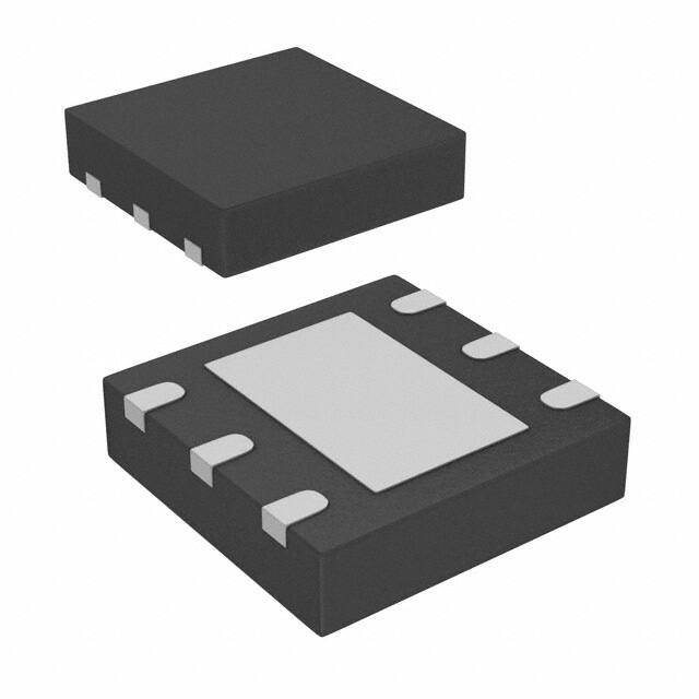
The MP2670 is available in a 10-pin 3mm x
3mm QFN package.
Cell Phones
MP3 Players
Smart Phones
PDA
Digital Cameras
Desktop Chargers
“MPS” and “The Future of Analog IC Technology” are Registered Trademarks of
Monolithic Power Systems, Inc.
TYPICAL APPLICATION
INPUT
VIN
OUT
CIN
COUT
LINEAR
BATTERY
CHARGER
MP2670
ILIM
VB
RILIM
EN
GND
FLT
RVB
BATTERY
PACK
+
RFLT
MP2670 Rev. 0.91
5/13/2010
www.MonolithicPower.com
MPS Proprietary Information. Unauthorized Photocopy and Duplication Prohibited.
© 2010 MPS. All Rights Reserved.
1
�MP2670 – CHARGE SYSTEM PROTECTION CIRCUIT
ORDERING INFORMATION
Part Number*
MP2670DQ
Package
QFN10
(3mm x 3mm)
Top Marking
Temperature
X7
–40°C to +85°C
* For Tape & Reel, add suffix –Z (g. MP2670DQ–Z).For RoHS compliant packaging, add suffix –LF (e.g.
MP2670DQ–LF–Z)
PACKAGE REFERENCE
TOP VIEW
VIN
1
10
OUT
GND
2
9
OUT
FLT
3
8
ILIM
NC
4
7
VB
NC
5
6
EN
EXPOSED PAD
ON BACKSIDE
CONNECT TO GND
ABSOLUTE MAXIMUM RATINGS (1)
Recommended Operating Conditions
VIN to GND......................................–0.3V to 30V
OUT and VB to GND........................–0.3V to 7V
Other Pins (ILIM, FLT , EN ) ..........–0.3V to 5.5V
Junction Temperature ...............................150°C
Lead Temperature (Solder).......................260°C
Storage Temperature.............. –65°C to +150°C
Supply Voltage VIN ..........................4.3V to 5.5V
Operating Temperature............. –40°C to +85°C
MP2670 Rev. 0.91
5/13/2010
Thermal Resistance
(3)
θJA
(2)
θJC
QFN10 (3mm x 3mm) .............50 ...... 12 ... °C/W
Notes:
1) Exceeding these ratings may damage the device.
2) The device is not guaranteed to function outside of its
operating conditions.
3) Measured on JESD51-7, 4-layer PCB.
www.MonolithicPower.com
MPS Proprietary Information. Unauthorized Photocopy and Duplication Prohibited.
© 2010 MPS. All Rights Reserved.
2
�MP2670 – CHARGE SYSTEM PROTECTION CIRCUIT
ELECTRICAL CHARACTERISTICS
VIN = 5V, TA = +25°C, unless otherwise noted.
Parameter
Symbol
Condition
Min
Typ
Max
Units
3.0
V
Power-On Reset
VPOR
Rising VIN Threshold
2.45
POR Hysteresis
VIN Bias Current
IVIN
Protection
Input Over-voltage Protection
(OVP)
Input OVP Hysteresis
Input OVP Falling Threshold
Input OVP Propagation Delay
Over-current Protection
Overcurrent Protection Blanking
Time
Battery Over-voltage Protection
Threshold
Battery OVP Threshold
Hysteresis
Battery OVP Falling Threshold
Battery OVP Blanking Time
VB Pin Leakage Current
Over Temperature Protection
Rising Threshold
Over Temperature Protection
Falling Threshold
Logic
5.55
VOVP
6.0
V
1
1.10
mV
V
µs
A
5.45
IOCP
VVB = 3V, RILIM = 25kΩ
0.90
1.0
170
BTOCP
4.29
VBOVP
µs
4.475
BTBOVP
VVB = 4.4V
mV
180
20
V
µs
nA
150
°C
110
°C
1.5
100
Sink 5mA current
RDS(ON)
Measured at 500mA,
4.3
很抱歉,暂时无法提供与“MP2104DQT-LF-P”相匹配的价格&库存,您可以联系我们找货
免费人工找货- 国内价格 香港价格
- 500+12.84876500+1.64812
- 1000+12.463471000+1.59869
- 1500+12.270511500+1.57394
- 2500+12.056762500+1.54652
- 3500+11.931813500+1.53050
- 5000+11.811625000+1.51508
