MP23701
24V, 2A, 1.5MHz, Synchronous,
Step-Down LED Driver
DESCRIPTION
FEATURES
The MP23701 is a 24V, monolithic,
synchronous, step-down, white LED driver with
a built-in power MOSFET and rectifier. The
MP23701 can achieve up to 2A of continuous
output current with excellent load and line
regulation. Peak-current mode operation
provides fast transient response and easy loop
stabilization.
The MP23701 implements deep analog
dimming. Full protection features include cycleby-cycle peak-current limiting, output shortcircuit protection (SCP), open LED protection,
NTC thermal protection, and thermal shutdown.
The MP23701 requires a minimal number of
readily
available,
standard,
external
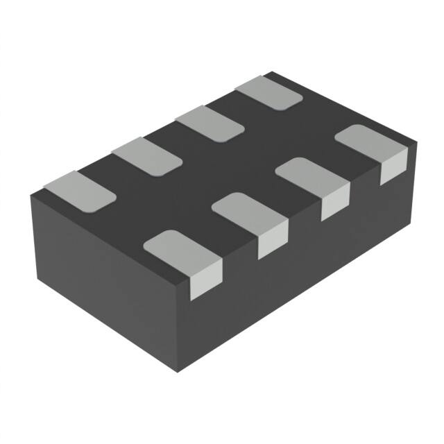
components and is available in a UTQFN-8
(1.5mmx2.5mm) package.
4.2V to 24V Wide Input Range
Synchronous Step-Down Converter
100mΩ Internal High-Side Power MOSFET
80mΩ Internal Low-Side Synchronous
Rectifier
Peak-Current Mode Control
Up to 2A Continuous Output Current
100mV Feedback Voltage
Up to 97% Efficiency
Fixed 1.5MHz Switching Frequency
Analog Dimming
Cycle-by-Cycle Current Limit
Inherent LED Open Protection
Output Short-Circuit Protection (SCP)
NTC Thermal Protection
Thermal Shutdown
Auto-Restart Function
Available in a UTQFN-8 (1.5mmx2.5mm)
Packages
APPLICATIONS
Infrared LED Drivers
General LED Drivers
Flashlights
Handheld Computer Backlight
All MPS parts are lead-free, halogen-free, and adhere to the RoHS
directive. For MPS green status, please visit the MPS website under
Quality Assurance. “MPS”, the MPS logo, and “Simple, Easy Solutions” are
trademarks of Monolithic Power Systems, Inc. or its subsidiaries.
TYPICAL APPLICATION
100
98
96
94
92
90
88
86
84
MP23701 Rev. 1.0
3/22/2019
6 8 10 12 14 16 18 20 22 24 26
VIN (V)
www.MonolithicPower.com
MPS Proprietary Information. Patent Protected. Unauthorized Photocopy and Duplication Prohibited.
© 2019 MPS. All Rights Reserved.
1
�MP23701 – 24V, 2A, 1.5MHZ, SYNCHRONOUS, STEP-DOWN, LED DRIVER
ORDERING INFORMATION
Part Number
MP23701GQEU*
Package
UTQFN-8 (1.5mmx2.5mm)
Top Marking
See Below
* For Tape & Reel, add suffix –Z (e.g.: MP23701GQEU–Z).
TOP MARKING
HZ: Product code of MP23701GQEU
Y: Year code
W: Week code
LL: Lot number
PACKAGE REFERENCE
TOP VIEW
UTQFN-8 (1.5mmx2.5mm)
MP23701 Rev. 1.0
3/22/2019
www.MonolithicPower.com
MPS Proprietary Information. Patent Protected. Unauthorized Photocopy and Duplication Prohibited.
© 2019 MPS. All Rights Reserved.
2
�MP23701 – 24V, 2A, 1.5MHZ, SYNCHRONOUS, STEP-DOWN, LED DRIVER
PIN FUNCTIONS
Pin #
Name
1
NC
2
VIN
3
SW
4
GND
5
BST
6
EN/DIM
7
FB
8
NTC
Description
No connection.
Supply voltage. The MP23701 operates on a 4.2V to 24V unregulated input range.
An input capacitor is needed to prevent large voltage spikes from appearing at the
input.
Switch output.
Ground. GND is the voltage reference for the regulated output voltage. Pay careful
attention to GND during layout.
Bootstrap. Connect a capacitor between SW and BST to form a floating supply
across the power switch driver. This capacitor is needed to drive the power switch’s
gate above the supply voltage.
On/off control input and dimming command input. Leave EN/DIM floating or apply
a voltage higher than 0.59V on EN/DIM to turn on the MP23701. For analog dimming,
when the EN/DIM voltage rises up from 0.7V to 1.44V, the output current changes
from its minimum value to the full-scale LED current.
Current sense feedback voltage. The FB internal reference voltage is 0.1V.
LED temperature protection. Connect an NTC resistor from NTC to GND to reduce
the output current to protect the LED when the ambient temperature rises up at high
levels.
ABSOLUTE MAXIMUM RATINGS (1)
Thermal Resistance (4)
Supply voltage (VIN) ...................................... 26V
VSW ........................................ -0.3V to VIN + 0.3V
VBST........................................................ VSW + 6V
All other pins ................................... -0.3V to +6V
Continuous power dissipation (TA = 25°C) (2)
UTQFN-8 (1.5mm x 2.5mm) ..................... 1.39W
Junction temperature ................................ 150°C
Lead temperature...................................... 260°C
Storage temperature .................-65°C to +150°C
ESD capability human body mode ............ 2.0kV
UTQFN-8 (1.5mmx2.5mm) ...... 90 ..... 20 ... °C/W
Recommended Operating Conditions (3)
Supply voltage (VIN) ......................... 4.2V to 24V
Operating junction temp. (TJ) .. …-40°C to 125°C
MP23701 Rev. 1.0
3/22/2019
θJA
θJC
NOTES:
1) Exceeding these ratings may damage the device.
2) The maximum allowable power dissipation is a function of the
maximum junction temperature TJ (MAX), the junction-toambient thermal resistance θJA, and the ambient temperature
TA. The maximum allowable continuous power dissipation at
any ambient temperature is calculated by PD (MAX) = (TJ
(MAX)-TA)/θJA. Exceeding the maximum allowable power
dissipation produces an excessive die temperature, causing
the regulator to go into thermal shutdown. Internal thermal
shutdown circuitry protects the device from permanent
damage.
3) The device is not guaranteed to function outside of its
operating conditions.
4) Measured on JESD51-7, 4-layer PCB.
www.MonolithicPower.com
MPS Proprietary Information. Patent Protected. Unauthorized Photocopy and Duplication Prohibited.
© 2019 MPS. All Rights Reserved.
3
�MP23701 – 24V, 2A, 1.5MHZ, SYNCHRONOUS, STEP-DOWN, LED DRIVER
ELECTRICAL CHARACTERISTICS
Typical values are VIN = 12V, TJ = 25°C, unless otherwise noted. Minimum and maximum values
are at VIN = 12V, TJ = -40°C to +125°C, unless otherwise noted, guaranteed by characterization.
Parameters
Supply Voltage
Operating range
Turn-on threshold
Hysteretic voltage
Supply Current
Shutdown current
Quiescent current
Enable and Dimming (EN/DIM)
EN/DIM off threshold
EN/DIM on threshold
Turn-off delay time
EN/DIM pull-up current
Max analog dimming threshold
Min analog dimming threshold
Feedback (FB)
Feedback voltage
Feedback current
Power Switch
Symbol
Condition
Min
VIN
VIN_ON
VIN_HYS
After turn on
VIN rising edge
4.2
3.5
ISD
IQ
VEN_OFF
VEN_ON
tOFF_DELAY
IEN/DIM
VADIM_MAX
VADIM_MIN
VFB
IFB
High-side MOSFET on
resistance
RDS(ON)_H
Low-side synchronous rectifier
switch on resistance
RDS(ON)_L
Switch leakage
High-side current limit
Low-side current limit
OCP current threshold
Oscillator frequency
Maximum duty cycle
Minimum on time
Restart Timer
Hiccup timer at fault condition
Bootstrap
Bias voltage for high-side
driver
MP23701 Rev. 1.0
3/22/2019
ISW_LKG
ILIMIT_H
ILIMIT_L
IOCP
fSW
DMAX
tON_MIN
Max
Units
24
4
V
V
V
10
0.9
50
1.1
μA
mA
0.27
0.545
16
2.8
1.31
0.63
0.31
0.59
22
3.8
1.44
0.7
0.35
0.635
28
5.3
1.57
0.78
V
V
ms
μA
V
V
93
100
30
107
75
mV
nA
100
110
80
90
170
180
140
150
1.5
6.6
-330
7
1.6
mΩ
mΩ
mΩ
mΩ
μA
A
mA
A
MHz
%
ns
VEN = 0V
VEN = 2V, VFB = 200mV
VEN/DIM falling edge
VEN/DIM rising edge
VEN = 0V
Theoretically, VFB = 100mV
VFB = 5mV
4.2V ≤ VIN ≤ 24V
VFB = 150mV
VIN = 5.0V
VIN = 4.2V
VIN = 5.0V
VIN = 4.2V
VEN = 0V, VSW = 0V
When high-side switch turns on
When low-side switch turns on
Both for high-side and low-side
VFB = 80mV
VFB = 80mV
3.5
-890
3.6
1.24
84
tSTART
VBST-VSW
Typ
3.7
0.12
5
-630
5.5
1.42
89
70
2.4
5.5V ≤ VIN ≤ 24V
VIN = 4.2V
4.8
3.6
5.1
www.MonolithicPower.com
MPS Proprietary Information. Patent Protected. Unauthorized Photocopy and Duplication Prohibited.
© 2019 MPS. All Rights Reserved.
ms
5.5
V
V
4
�MP23701 – 24V, 2A, 1.5MHZ, SYNCHRONOUS, STEP-DOWN, LED DRIVER
ELECTRICAL CHARACTERISTICS (continued)
Typical values are VIN = 12V, TJ = 25°C, unless otherwise noted. Minimum and maximum values
are at VIN = 12V, TJ = -40°C to +125°C, unless otherwise noted, guaranteed by characterization.
Parameters
NTC
High-threshold voltage
Low-threshold voltage
Shutdown threshold
Shutdown voltage hysteresis
Pull-up current source
Leakage current
Thermal Shutdown
Thermal shutdown threshold (5)
Thermal shutdown hysteresis
(5)
Symbol
Condition
Min
Typ
Max
Units
VH_NTC
VL_NTC
VSD_NTC
VFB = 95mV
VFB = 5mV
VNTC falling edge
1.05
0.76
0.34
55
41
1.15
0.82
0.41
110
58
1.25
0.88
0.47
185
72
1
V
V
V
mV
μA
μA
VSD_NTC_HYS
IPULL_UP_NTC
INTC_LKG
TSD
150
°C
THYS
60
°C
NOTE:
5) Guaranteed by characterization.
MP23701 Rev. 1.0
3/22/2019
www.MonolithicPower.com
MPS Proprietary Information. Patent Protected. Unauthorized Photocopy and Duplication Prohibited.
© 2019 MPS. All Rights Reserved.
5
�MP23701 – 24V, 2A, 1.5MHZ, SYNCHRONOUS, STEP-DOWN, LED DRIVER
TYPICAL CHARACTERISTICS
103
102
180
160
160
140
140
120
120
100
100
80
80
60
101
100
99
98
97
96
95
-50 -25 0
MP23701 Rev. 1.0
3/22/2019
25 50 75 100 125 150
60
-50 -25 0
25 50 75 100 125 150
40
-50 -25 0
25 50 75 100 125 150
www.MonolithicPower.com
MPS Proprietary Information. Patent Protected. Unauthorized Photocopy and Duplication Prohibited.
© 2019 MPS. All Rights Reserved.
6
�MP23701 – 24V, 2A, 1.5MHZ, SYNCHRONOUS, STEP-DOWN, LED DRIVER
TYPICAL PERFORMACE CHARACTERISTICS
Performance waveforms are tested on the evaluation board.
VIN = 12V, 2 WLEDs in series, VOUT = 5.9V, ILED = 1.5A, L = 4.7μH, TA = 25°C, unless otherwise
noted.
Efficiency vs. VIN
Line Regulation
2 WLEDs in series
2 WLEDs in series
1.6
100
100
98
97
96
94
0.8
94
91
0.4
92
88
1.2
VIN=5V
0.0
VIN=12V
90
85
88
82
-0.8
86
79
-1.2
84
76
6 8 10 12 14 16 18 20 22 24 26
VIN (V)
-0.4
-1.6
0 1 2 3 4 5 6 7 8 9 10 11
VOUT (V)
Analog Dimming Curve
1.6
1.6
0.6
1.4
1.4
1.2
ILED (A)
0.2
0.0
-0.2
VIN=12V
-0.4
-0.6
-0.8
0 1 2 3 4 5 6 7 8 9 10 11
VOUT (V)
MP23701 Rev. 1.0
3/22/2019
1.2
VDIM Falling
1.0
0.8
0.6
ILED (A)
VIN=5V
8 10 12 14 16 18 20 22 24 26
VIN (V)
NTC Curve
0.8
0.4
6
1.0
0.8
0.6
0.4 VDIM Rising
0.4
0.2
0.2
0.0
0.2 0.4 0.6 0.8 1 1.2 1.4 1.6
VDIM ANALOG LEVEL (V)
0.0
0.3
0.5
0.7 0.9 1.1 1.3
VNTC LEVEL (V)
www.MonolithicPower.com
MPS Proprietary Information. Patent Protected. Unauthorized Photocopy and Duplication Prohibited.
© 2019 MPS. All Rights Reserved.
1.5
7
�MP23701 – 24V, 2A, 1.5MHZ, SYNCHRONOUS, STEP-DOWN, LED DRIVER
TYPICAL PERFORMACE CHARACTERISTICS (continued)
Performance waveforms are tested on the evaluation board.
VIN = 12V, 2 WLEDs in series, VOUT = 6V, ILED = 1A, L = 3.3μH, TA = 25°C, unless otherwise noted.
MP23701 Rev. 1.0
3/22/2019
www.MonolithicPower.com
MPS Proprietary Information. Patent Protected. Unauthorized Photocopy and Duplication Prohibited.
© 2019 MPS. All Rights Reserved.
8
�MP23701 – 24V, 2A, 1.5MHZ, SYNCHRONOUS, STEP-DOWN, LED DRIVER
BLOCK DIAGRAM
Figure 1: Functional Block Diagram
MP23701 Rev. 1.0
3/22/2019
www.MonolithicPower.com
MPS Proprietary Information. Patent Protected. Unauthorized Photocopy and Duplication Prohibited.
© 2019 MPS. All Rights Reserved.
9
�MP23701 – 24V, 2A, 1.5MHZ, SYNCHRONOUS, STEP-DOWN, LED DRIVER
OPERATION
The MP23701 is a high-frequency, synchronous,
rectified, step-down, switch-mode LED driver
with a built-in, internal power MOSFET and
synchronous rectifier switch. The MP23701
offers a very high-performance solution that
achieves up to 2A of continuous output LED
current with excellent load and line regulation
over a wide input supply range.
Three events can shut down the chip: EN/DIM
dropping low for longer than tOFF_DELAY, VIN
dropping below UVLO, and thermal shutdown.
During the shutdown procedure, the signaling
path is blocked first to prevent any fault
triggering. The COMP voltage (VCOMP) and the
internal supply rail are then pulled down.
The MP23701 operates with a fixed 1.5MHz
frequency and uses peak-current control mode
to regulate the output current. A new switching
cycle is initiated by the internal clock at the
beginning of every switching cycle.
Error Amplifier (EA)
The internal, low, offset error amplifier
compares the FB voltage with the internal
100mV reference and outputs a VCOMP value in
the chip internally. This VCOMP value is used to
control the HS-FET peak current and regulate
the output current.
The integrated high-side power MOSFET (HSFET) is turned on, and the inductor current rises
linearly to provide energy to the load. The HSFET remains on until its current reaches the
value of the COMP level, which is the output of
the internal error amplifier. The output voltage
of the error amplifier depends on the difference
of the output feedback and the internal, highprecision reference.
Internal Soft Start (SS)
Soft start (SS) is implemented to prevent the
converter output current from overshooting
during start-up. When the chip starts up, the
internal circuitry generates a soft-start voltage
that ramps up from 0V. The soft-start period
lasts until the voltage on the soft-start capacitor
exceeds the 0.1V reference voltage. At this
point, the reference voltage takes over.
The HS-FET remains off until the next clock
cycle begins. After the HS-FET turns off, the
low-side sync switch (LS-FET) turns on, and the
inductor current flows through the LS-FET. To
prevent shoot-through, a dead time is
implemented to prevent the HS-FET and LSFET from turning on at the same time.
Floating Driver and Bootstrap Charging
The high-side, floating, power MOSFET driver
is powered by an external bootstrap capacitor.
The bootstrap capacitor voltage is regulated
internally. During normal operation, a 5.1V
bootstrap voltage is maintained between BST
and SW.
If the duty cycle reaches 94% in one switching
period, the current in the HS-FET cannot reach
the COMP-set current value, and the HS-FET is
forced to turn off.
Enable and Dimming Control (EN/DIM)
EN/DIM is a control pin that turns the regulator
on and off and dims the output LED current
through a DC signal. Leave EN/DIM floating or
drive it high to turn on the MP23701. After
EN/DIM is pulled low for tOFF_DELAY (typically
22ms), the MP23701 is turned off. Figure 2
shows the control logic of EN/DIM.
Under-Voltage Lockout (UVLO) and IC StartUp/Shutdown Procedure
Under-voltage lockout (UVLO) is implemented
to prevent the chip from operating at an
insufficient supply voltage. The MP23701 UVLO
comparator monitors the output voltage of the
internal regulator, which is supplied from VIN.
If both VIN and EN/DIM are higher than their
appropriate thresholds, the chip starts up. The
reference block starts first to generate a stable
reference voltage and current. The internal
regulator is then enabled. The regulator
provides a stable supply for the remaining
circuitries.
MP23701 Rev. 1.0
3/22/2019
Figure 2: EN/DIM Time Sequence
www.MonolithicPower.com
MPS Proprietary Information. Patent Protected. Unauthorized Photocopy and Duplication Prohibited.
© 2019 MPS. All Rights Reserved.
10
�MP23701 – 24V, 2A, 1.5MHZ, SYNCHRONOUS, STEP-DOWN, LED DRIVER
Analog Dimming
Apply a DC signal on EN/DIM to dim the
MP23701 in analog dimming mode. When the
voltage on EN/DIM is lower than VADIM_MIN, the
LED current is regulated to the minimum scale.
When the voltage on EN/DIM is between
VADIM_MIN and VADIM_MAX, the LED current
changes from the minimum scale to the full
scale of the LED current. If the voltage on
EN/DIM is higher than VADIM_MAX, the maximum
LED current is regulated.
Figure 3 shows the analog dimming curve. Due
to the hysteretic of the EN/DIM on/off threshold,
the chip remains at the minimal LED current
longer at the VEN/DIM falling edge until VEN/DIM is
lower than VEN_OFF. The dimming curve is the
same as in the linear dimming range.
In the worst-case scenario, the LED is shorted
to GND. If the cycle-by-cycle current-limit
function cannot clamp the current overshoot
sufficiently, then the current through both the
HS-FET and LS-FET is also monitored by the
over-current detector inside the chip. If this
current is higher than the short-circuit threshold
(IOCP), the MP23701 treats this as a short-circuit
condition.
When an over-current condition or short-circuit
condition is detected, the MP23701 turns off
both the HS-FET and LS-FET for 2.4ms and
restarts. During this period, VCOMP is pulled
down to ground, so the restart from the fault
condition is also done with a soft start.
Thermal Protection
NTC provides LED thermal protection. An NTC
resistor used to monitor the ambient
temperature can be connected to NTC directly.
There is an internal current source flowing out
of NTC. The corresponding voltage is
generated on the external NTC resistor and the
LED current changes (see Figure 4).
Figure 3: Analog Dimming Curve
Open LED
If the LED is open without a feedback signal,
the MP23701 works at the maximum duty cycle,
and the output voltage rises up almost to the
input voltage. Every power component operates
at a safe state.
LED Short-Circuit Protection (SCP)
The MP23701 integrates LED short-circuit
protection (SCP) circuitry. There are several
features protecting the MP23701 from damage
when an LED short circuit occurs.
The MP23701 uses a cycle-by-cycle current
limit to restrict the maximum current of the
inductor. A protection mechanism monitors the
FB level though an internal R-C filter. Once the
FB level rises up to VFB_BURST_AL, the chip stops
switching until the FB level drops to a lower
value, and the system works in burst mode.
MP23701 Rev. 1.0
3/22/2019
Figure 4: NTC Curve
The NTC resistance value drops when the
ambient temperature rises up. If the NTC
voltage drops below VSD_NTC, the switching
stops completely, and the LED current drops to
0A, so the LED lamp can be shut down by
pulling NTC down.
Additionally, to protect against any lethal
thermal damage, when the inner temperature
exceeds the over-temperature protection (OTP)
threshold, the MP23701 uses thermal shutdown
to shut down the switching cycle until the
temperature drops to its lower threshold.
www.MonolithicPower.com
MPS Proprietary Information. Patent Protected. Unauthorized Photocopy and Duplication Prohibited.
© 2019 MPS. All Rights Reserved.
11
�MP23701 – 24V, 2A, 1.5MHZ, SYNCHRONOUS, STEP-DOWN, LED DRIVER
Thermal Shutdown
Thermal shutdown is implemented to prevent
the chip from operating at exceedingly high
temperatures. When the silicon die temperature
is higher than 150°C, OTP shuts down the
entire chip. When the temperature is below its
lower threshold (typically 90°C), the chip
restarts.
MP23701 Rev. 1.0
3/22/2019
www.MonolithicPower.com
MPS Proprietary Information. Patent Protected. Unauthorized Photocopy and Duplication Prohibited.
© 2019 MPS. All Rights Reserved.
12
�MP23701 – 24V, 2A, 1.5MHZ, SYNCHRONOUS, STEP-DOWN, LED DRIVER
APPLICATION INFORMATION
Setting the LED Current
A current sense resistor is inserted between the
anode of LED and GND. The current sense
resistor value can be calculated with Equation
(1):
RS
0.1V
ILED
(1)
For a 2A LED current output, RS is 50mΩ.
Selecting the Inductor
An inductor less than 100µH with a nominal DC
current rating at least 25% higher than the
maximum load current is recommended for
most applications. For the highest efficiency,
the inductor’s DC resistance should be less
than 100mΩ. For most designs, the required
inductance value can be derived from Equation
(2):
L
VOUT (VIN VOUT )
VIN IL fSW
(2)
Where ∆IL is the inductor ripple current.
Choose the inductor ripple current to be 30% of
the maximum load current. The maximum
inductor peak current can be calculated with
Equation (3):
IL(MAX) ILED
IL
2
Selecting the Output Capacitor
The output capacitor keeps the output current
ripple small and ensures feedback loop stability.
The output capacitor impedance should be low
at the switching frequency. Ceramic capacitors
with X5R or X7R dielectrics are recommended
for their low ESR characteristics. For most
applications, a 10µF ceramic capacitor is
sufficient.
PCB Layout Guidelines
Efficient PCB layout is critical for stable
operation. For best results, follow the guidelines
below.
1. Place the high-current paths (GND, VIN,
and SW) very close to the device with short,
direct, and wide traces.
2. Place the input capacitor as close to VIN
and GND as possible.
3. Place the external feedback resistors next
to FB.
4. Keep the switch node traces short and away
from the feedback network.
For more information, please refer to the related
evaluation board datasheet.
(3)
Selecting the Input Capacitor
The input capacitor reduces the surge current
drawn from the input supply and the switching
noise from the device. The input capacitor
impedance at the switching frequency should
be less than the source impedance to prevent
the high-frequency switching current from
passing through the input. Ceramic capacitors
with X5R or X7R dielectrics are highly
recommended because of their low ESR and
small temperature coefficients. For most
applications, a 10µF capacitor is sufficient.
MP23701 Rev. 1.0
3/22/2019
www.MonolithicPower.com
MPS Proprietary Information. Patent Protected. Unauthorized Photocopy and Duplication Prohibited.
© 2019 MPS. All Rights Reserved.
13
�MP23701 – 24V, 2A, 1.5MHZ, SYNCHRONOUS, STEP-DOWN, LED DRIVER
TYPICAL APPLICATION CIRCUIT
Figure 5: Typical Buck Converter Application, VIN = 5V to 24V, 1-2 WLEDs in series, ILED = 1A
MP23701 Rev. 1.0
3/22/2019
www.MonolithicPower.com
MPS Proprietary Information. Patent Protected. Unauthorized Photocopy and Duplication Prohibited.
© 2019 MPS. All Rights Reserved.
14
�MP23701 – 24V, 2A, 1.5MHZ, SYNCHRONOUS, STEP-DOWN, LED DRIVER
PACKAGE INFORMATION
UTQFN-8 (1.5mmx2.5mm)
NOTICE: The information in this document is subject to change without notice. Please contact MPS for current specifications.
Users should warrant and guarantee that third party Intellectual Property rights are not infringed upon when integrating MPS
products into any application. MPS will not assume any legal responsibility for any said applications.
MP23701 Rev. 1.0
3/22/2019
www.MonolithicPower.com
MPS Proprietary Information. Patent Protected. Unauthorized Photocopy and Duplication Prohibited.
© 2019 MPS. All Rights Reserved.
15
�