MP24971
1.5A, 50V, 100kHz, 5V Fixed Output StepDown Converter with Programmable Current
Limit and Output Line-Drop Compensation
The Future of Analog IC Technology
DESCRIPTION
FEATURES
The MP24971 is a monolithic, step-down,
switch-mode converter with a programmable
output-current limit. It has a fixed 5V/1.5A
continuous output over a wide input supply
range, and has excellent load and line
regulation. It has an internal 2ms-to-4ms softstart that prevents inrush current at start-up,
and compensates for output line drop.
MP24971 achieves a low EMI signature with
well-controlled switching edges.
It has fault-condition protections including
hiccup-mode current limit protection, shortcircuit
protection,
output
over-voltage
protection, and thermal shutdown.
The MP24971 requires a minimal number of
readily-available standard external components,
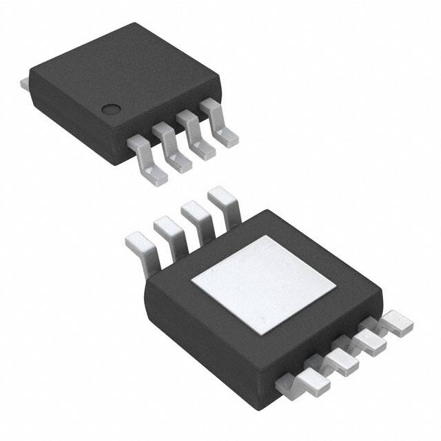
and is available in SOIC8 and SOIC8E
packages.
Wide 8V-to-50V Operating Input Range
Output Over-Voltage Protection
5V Fixed Output
0.4Ω Internal Power MOSFET
Internal 4ms Soft-Start
Stable with Low-ESR Ceramic Output
Capacitors
Fixed 100kHz Frequency
Low EMI Signature
Thermal Shutdown
Output Line-Drop Compensation
Hiccup Circuit Limit and Short Circuit
Protection
Available in SOIC8 and SOIC8E Package
APPLICATIONS
USB Power Supplies
Automotive Power Adapters
Power Supplies for Linear Chargers
All MPS parts are lead-free and adhere to the RoHS directive. For MPS green
status, please visit MPS website under Products, Quality Assurance page.
“MPS” and “The Future of Analog IC Technology” are registered trademarks of
Monolithic Power Systems, Inc.
TYPICAL APPLICATION
Efficiency vs.
Output Current
R1
0O
C2
2.2µF
VIN
C1
220µF
BST
L1
33µH
C8
C9
C7
100µF 22µF 0.1µF
+
Diode
C3
0.1µF
VOC
GND
R2
402kO
MP24971
ISP
GND
ISN
C5
10nF
R3
1kO
C6
10nF
R4
1kO
C10
0.1µF
VOUT=5V
VIN=12V
90
V OUT
SW
VIN
VOS
95
RSENSE
66mO
EFFICIENCY (%)
C4
0.1µF
85
80
VIN=24V
75
70
65
VIN=50V
60
R5
0O
55
0.1 0.3 0.5 0.7 0.9 1.1 1.3 1.5
OUTPUT CURRENT (A)
MP24971 Rev. 1.01
www.MonolithicPower.com
1/6/2012
MPS Proprietary Information. Patent Protected. Unauthorized Photocopy and Duplication Prohibited.
© 2012 MPS. All Rights Reserved.
1
�MP24971 –1.5A, 50V, 100kHz, 5V FIXED OUTPUT STEP-DOWN CONVERTER
ORDERING INFORMATION
Part Number
MP24971DS*
MP24971DN**
Package
SOIC8
SOIC8E
Top Marking
MP24971
MP24971
Operating Temperature (TJ)
-40C to +125C
-40C to +125C
* For Tape & Reel, add suffix –Z (eg. MP24971DS–Z);
For RoHS, compliant packaging, add suffix –LF (eg. MP24971DS–LF–Z).
** For Tape & Reel, add suffix –Z (eg. MP24971DN–Z);
For RoHS, compliant packaging, add suffix –LF (eg. MP24971DN–LF–Z).
PACKAGE REFERENCE
SOIC8
ABSOLUTE MAXIMUM RATINGS (1)
Input Voltage VIN .......................................... 60V
VISN, VISP, VVOS ........................................ 0V to 8V
|VISN -VISP| ........................................... 0V to 0.4V
VSW ..................................... -0.3V to (VIN + 0.3V)
VBST ................................................... VSW + 6.5V
All Other Pins ...............................-0.3V to +6.5V
Junction Temperature ...............................150°C
Lead Temperature ....................................260°C
Storage Temperature ............... -65°C to +150°C
(2)
Continuous Power Dissipation (TA = 25°C)
SOIC8 ...................................................... 1.38W
SOIC8E ...................................................... 2.5W
ESD Susceptibility
HBM (Human Body Mode).......................... 2kV
SOIC8E
Recommended Operating Conditions
(3)
Input Voltage VIN ................................. 8V to 50V
Maximum Junction Temp. (TJ) ................ 125°C
Thermal Resistance
(4)
θJA
θJC
SOIC8 ..................................... 90 ...... 45... °C/W
SOIC8E .................................. 50 ...... 10... °C/W
Notes:
1) Exceeding these ratings may damage the device.
2) The maximum allowable power dissipation is a function of the
maximum junction temperature TJ (MAX), the junction-toambient thermal resistance θJA, and the ambient temperature
TA. The maximum allowable continuous power dissipation at
any ambient temperature is calculated by PD (MAX) = (TJ
(MAX)-TA)/θJA. Exceeding the maximum allowable power
dissipation will cause excessive die temperature, and the
regulator will go into thermal shutdown. Internal thermal
shutdown circuitry protects the device from permanent
damage.
3) The device is not guaranteed to function outside of its
operating conditions.
4) Measured on JESD51-7, 4-layer PCB.
MP24971 Rev. 1.01
www.MonolithicPower.com
1/6/2012
MPS Proprietary Information. Patent Protected. Unauthorized Photocopy and Duplication Prohibited.
© 2012 MPS. All Rights Reserved.
2
�MP24971 –1.5A, 50V, 100kHz, 5V FIXED OUTPUT STEP-DOWN CONVERTER
ELECTRICAL CHARACTERISTICS
VIN = 12V, TA = 25°C, unless otherwise noted.
Parameters
Symbol
Output Voltage
VOUT
Output Over-Voltage
Protection
VOVP
Switch-On Resistance
Condition
Min
Typ
Max
Units
8V VIN 50V, RSENSE=0Ω
4.85
5
5.15
V
5.69
6
6.2
V
0.4
0.5
Ω
0.1
(5)
1
μA
3.5
4.4
5.2
A
70
100
140
kHz
RDS(ON)
Switch Leakage
VISN = 6.5V, VSW = 0V
Current Limit
Oscillator Frequency
fSW
Bootstrap Voltage
VBST - VSW
Minimum On Time
tON
SW Rising Edge
SW Falling Edge
4
50
100
250
ns
tRISE
50
100
ns
tFALL
85
150
ns
3.5
4.2
V
Under-Voltage Lockout Threshold
Rising
Under-Voltage Lockout Threshold
Hysteresis
Load-Line Compensation
Gain
Current Sense Voltage
Input Bias Current (ISN, ISP)
Supply Current (Quiescent)
Thermal Shutdown
V
2.8
200
VVOC
mV
VISP-VISN=50mV
200
330
450
VISP-VISN=100mV
500
620
700
90
-1
100
-0.5
110
+1
mV
μA
1.2
1.5
mA
VISP-VISN VISN=5V
IBIAS (ISN,ISP) VISP=VISN=5V
VISN = VVOS = 5.5V
150
mV
°C
Note:
5) Guaranteed by design.
MP24971 Rev. 1.01
www.MonolithicPower.com
1/6/2012
MPS Proprietary Information. Patent Protected. Unauthorized Photocopy and Duplication Prohibited.
© 2012 MPS. All Rights Reserved.
3
�MP24971 –1.5A, 50V, 100kHz, 5V FIXED OUTPUT STEP-DOWN CONVERTER
PIN FUNCTIONS
Package
Pin #
1
2
3
4
5
6
7
8
Name
Description
Supply Voltage. Operates from an unregulated 8V-to-50V input. Requires decoupling
capacitor(s)—CIN—to limit voltage spikes. Drain of the internal power MOSFET; supplies
power to the whole chip.
Ground. Voltage reference of the regulated output voltage. GND node should be placed
GND
outside of the diode-to-CIN ground path to prevent switching current spikes from inducing
Exposed
voltage noise into the part. Connect exposed pad to GND plane for optimal thermal
Pad
performance.
VOS
Output Voltage Sense. Connect directly to the output.
Output Line Drop Compensator. Connect to GND through a resistor to compensate for the
VOC
output voltage drop.
Negative Current Sense Input. Used for limiting load current and for over-voltage
ISN
protection. Native 6V over-voltage protection threshold.
ISP
Positive Current Sense Input. Used for load current limiting.
Bootstrap. Requires a capacitor to drive the power MOSFET gate above the supply
voltage. Connected capacitor between SW and BST pins to form a floating supply across
BST
the power MOSFET driver. An on-chip regulator charges the external bootstrap capacitor.
If the on-chip regulator is not powerful enough, add a diode from VIN or VOUT to charge the
external boot-strap capacitor.
VIN
SW
Switch Output. Output power supply.
MP24971 Rev. 1.01
www.MonolithicPower.com
1/6/2012
MPS Proprietary Information. Patent Protected. Unauthorized Photocopy and Duplication Prohibited.
© 2012 MPS. All Rights Reserved.
4
�MP24971 –1.5A, 50V, 100kHz, 5V FIXED OUTPUT STEP-DOWN CONVERTER
TYPICAL CHARACTERISTICS
IBIAS(ISP,ISN) vs.
Temperature
Current Limit vs.
Temperature
V =V =5V
-0.45 ISP ISN
-0.5
5.4
4.96
5.3
4.9575
5.2
-0.6
-0.65
-0.7
-0.75
-0.8
4.9525
5
4.9
4.8
4.945
4.6
4.9425
4.5
-20
10
40
4.4
-50
70 100 130
4.95
4.9475
4.7
-20
10
40
4.94
-50
70 100 130
VOVP vs. Temperature
Frequency vs. Temperature
109
106
105
104
5.94
5.93
5.92
103
102
40
70 100 130
635
VVOC(mV)
VOVP(V)
107
10
VISP-VISN=100mV
640
5.95
108
-20
VVOC vs. Temperature
5.96
110
FREQUENCY(kHz)
4.955
5.1
VVOS(V)
CURRENT LIMIT(A)
-0.55
-0.85
-50
VVOS vs. Temperature
630
625
620
5.91
101
-20
10
40
70 100 130
5.9
-50
VBST vs. Temperature
1220
4.1
4
VBST(V)
10
40
615
-50
70 100 130
104
1190
103.5
1160
1150
3.85
10
40
70 100 130
1130
-50
70 100 130
103
102.5
102
101.5
101
1140
-20
40
VISN=5V
105
1200
1170
3.9
10
104.5
1180
3.95
-20
VISP-VISN vs. Temperature
Quiescent Current vs.
Temperature
1210
4.05
3.8
-50
-20
VISP-VISN(mV)
100
-50
100.5
-20
10
40
70 100 130
100
-50
-20
10
40
MP24971 Rev. 1.01
www.MonolithicPower.com
1/6/2012
MPS Proprietary Information. Patent Protected. Unauthorized Photocopy and Duplication Prohibited.
© 2012 MPS. All Rights Reserved.
70 100 130
5
�MP24971 –1.5A, 50V, 100kHz, 5V FIXED OUTPUT STEP-DOWN CONVERTER
TYPICAL PERFORMANCE CHARACTERISTICS
C1=220μF, C2=2.2μF, C8=22μF, C9=100μF, L=33μH, RSENSE=66mΩ, TA=25°C, unless otherwise
noted.
Output Line Drop
Loop Gain with
Efficiency vs.
Compensation
Phase Margin
Output Current
4.95
VIN=24V
4.93
GAIN (dB)
VOUT (V)
4.94
VIN=50V
4.92
4.91
4.9
0 0.2 0.4 0.6 0.8 1 1.2 1.4
IOUT (A)
95
40
160
90
30
120
20
80
10
40
0
0
-10
-40
-20
-80
-30
-120
-40
-160
-50
0.1
Load Regulation
1
10
100
FREQUENCY(kHz)
-200
1000
VIN=12V
85
80
VIN=24V
75
70
65
VIN=50V
60
55
0.1 0.3 0.5 0.7 0.9 1.1 1.3 1.5
IOUT (A)
EMI Radiation
Connect ISP, ISN to GND
90
4.96
VOUT=5V
200
50
VIN=12V
VIN=12V, VOUT=5V, IOUT=1.5A
Resistor Load
PHASE (degree)
4.96
VIN=12V, VOUT=5V, IOUT=1.5A
Resistor Load
80
VOUT (V)
4.955
VIN=24V
VIN=12V
60
4.95
4.945
70
50
EN55022
40
VIN=50V
4.94
4.935
4.93
0 0.2 0.4 0.6 0.8 1 1.2 1.4 1.6
IOUT (A)
30
20
10
0
-10
30
100
FREQUENCY(MHz)
1000
MP24971 Rev. 1.01
www.MonolithicPower.com
1/6/2012
MPS Proprietary Information. Patent Protected. Unauthorized Photocopy and Duplication Prohibited.
© 2012 MPS. All Rights Reserved.
6
�MP24971 –1.5A, 50V, 100kHz, 5V FIXED OUTPUT STEP-DOWN CONVERTER
TYPICAL PERFORMANCE CHARACTERISTICS (continued)
C1=220μF, C2=2.2μF, C8=22μF, C9=100μF, L=33μH, RSENSE=66mΩ, TA=25°C,unless otherwise
noted.
Steady State
Steady State
Power Ramp Up
VIN=12V, VOUT=5V, IOUT=1.5A E-Load
VIN=50V, VOUT=5V, IOUT=1.5A E-Load
SW
10V/div
VIN/AC
500mV/div
SW
50V/div
VIN/AC
1V/div
VOUT/AC
20mV/div
VOUT/AC
50mV/div
IL
2A/div
IL
2A/div
VIN
10V/div
SW
10V/div
VOUT
5V/div
IOUT
2A/div
Power Ramp Down
Short Circuit Enter
Short Circuit Steady
VIN=12V, VOUT=5V, IOUT=1.5A
Resistor Load
VIN=12V, VOUT=5V, IOUT=0.5A
VIN=12V, VOUT=5V
VIN
10V/div
SW
10V/div
SW
10V/div
SW
10V/div
VOUT
5V/div
VOUT
500mV/div
IL
2A/div
IOUT
2A/div
VOUT
5V/div
IOUT
2A/div
SW
10V/div
VIN=12V, VOUT=5V, IOUT=1.5A
Resistor Load
Short Circuit Recovery
Load Transient Response
Over Voltage Protection
VIN=12V, VOUT=5V, IOUT=0.5A
VIN=12V, VOUT=5V, IOUT=0.3A-1.5A
Slew Rate=6.4mA/ s
VIN=12V, VOUT=5V, IOUT=1.5A
Add an 6V External Power to ISN
VOUT
200mV/div
VISN
5V/div
VOUT
5V/div
SW
10V/div
IOUT
2A/div
VOUT
5V/div
IOUT
2A/div
IOUT
1A/div
MP24971 Rev. 1.01
www.MonolithicPower.com
1/6/2012
MPS Proprietary Information. Patent Protected. Unauthorized Photocopy and Duplication Prohibited.
© 2012 MPS. All Rights Reserved.
7
�MP24971 –1.5A, 50V, 100kHz, 5V FIXED OUTPUT STEP-DOWN CONVERTER
FUNCTIONAL BLOCK DIAGRAM
VIN
CURRENT SENSE
AMPLIFIER
GND
Σ
REGULATOR
63mO
BST
RAMP
REFERENCE
NMOSFET
REGULATOR
OSCILLATOR
DRIVER
CLK
RSENSE OUT
SW
S
IN
Q
R
PWM
COMPARATOR
600mV
6.2uA
200mV
JFET
Hiccup
Current Limit
ISP
X6
ISN
RS1
RS2
VOS
1.23V
OVP
COMPARATOR
C2
50pF
R1
1704kO
10000kO
RTOP
300kO
JFET
C1
1pF
SS Circuit
ERROR
AMPLIFIER
800mV
10pF
VOC
RBOT
57.14kO
RC
Figure 1—Function Block Diagram
MP24971 Rev. 1.01
www.MonolithicPower.com
1/6/2012
MPS Proprietary Information. Patent Protected. Unauthorized Photocopy and Duplication Prohibited.
© 2012 MPS. All Rights Reserved.
8
�MP24971 –1.5A, 50V, 100kHz, 5V FIXED OUTPUT STEP-DOWN CONVERTER
OPERATION
Main Control Loop
The MP24971 is a current-mode buck regulator
where the output voltage of the error amplifier
(EA) is proportional to the peak inductor
current.
When a cycle starts, SW is disconnected and
the EA output voltage is higher than the current
sense amplifier (CSA) output. The rising edge
of the 100kHz CLK signal sets the RS flip-flop,
which connects SW and the inductor to the
input supply.
The CSA amplifies the rising inductor current.
The PWM comparator (PWMCOMP) compares
sum of the CSA output and the ramp
compensation (positive input) against the EA
output (negative input). When the positive
PWMCOMP input exceeds the negative PWMCOMP
input, the RS flip-flop resets and the MP24971
reverts to its initial SW off state: Otherwise, the
falling edge of the CLK resets the flip-flop.
The EA amplifies the voltage difference
between VOUT (connected through the VOS pin)
and the 800mV reference: Because VOUT
connects to the negative input of the EA, when
VOUT drops below 5V, the EA output increases.
Since the EA output voltage is proportional to
the peak inductor current, an increase in
inductor voltage increases current delivered to
the output. An external Schottky Diode
dissipates the inductor current when SW is off.
Hiccup-Mode Current Limit Protection
The ISP and ISN pins sense the output current
information for current limit protection. Once the
VSENSE exceeds the 100mV voltage limit
threshold, the current limit loop will turn off the
high-side MOSFET immediately. The internal
soft-start circuit resets after the VOS voltage
drops below 1.9V and VCOMP rises above 3V; at
this point, the high side switch turns on and
MP24971 restarts with a full soft start. This
hiccup process repeats until the device stops
detecting a fault.
The current limit value can be lowered by an
internal current source and external resistors
connected to ISN and ISP pins when the output
voltage drops below 200mV. This feature can
greatly reduce the average short circuit current.
Output Over-Voltage Protection
The MP24971 has output over-voltage
protection to prevent the output voltage from
rising above a threshold of 6V—such as if the
output sense is left open—and prevents any
voltage damage to the circuit load. If the output
voltage—as sensed by the ISN pin—rises
above 6V, the high-side MOSFET will turn off
immediately and part will be lathed off after a
timer delay.
Output-Line–Drop Compensation
MP24971 is capable of compensating an output
voltage drop—such as high impedance caused
by a very long trace—to keep a constant 5V
load-side voltage. Compensation feedback
comes from the VOS pin and through the RTOP
resistor. Program the load line compensation
gain using a resistor connected to VOC pin,
selected based on RSENSE and RTRACE (Figure 2)
values.
MP24971 Rev. 1.01
www.MonolithicPower.com
1/6/2012
MPS Proprietary Information. Patent Protected. Unauthorized Photocopy and Duplication Prohibited.
© 2012 MPS. All Rights Reserved.
9
�MP24971 –1.5A, 50V, 100kHz, 5V FIXED OUTPUT STEP-DOWN CONVERTER
APPLICATION INFORMATION
Setting the Output Line Drop Compensation
Long traces to the circuit load induce a voltage
drop between VOUT and VLOAD. that can be
described as:
VDROP IOUT RTRACE
Supplying an accurate and consistent load
voltage over current-dependant trace resistance
necessitates line-drop compeonsation.
MP24971 offers a compensation method that
adjusts the FB voltage slightly according to the
load current.
The relation between VOUT and VFB can be
described by:
(3)
IOUT RSENSE 6 RTOP
RC
(4)
The VLOAD is determined by:
VLOAD 5V
IOUT RSENSE 6 RTOP
RC
(5)
IOUT RTRACE
Load
X6
ISN
R TOP
VFB
VOS
VOC
RC
RBOT
Hiccup
Current Limit
600mV
10000kO
10pF
0.8V
ERROR
AMPLIFIER
Internal Block
Selecting the Inductor
For most applications, use a 10µH to 47µH
inductor with a DC current rating of at least
125% of the maximum load current. For best
efficiency, select an inductor with a DC
resistance less than 200mΩ. For most designs,
the inductance value can be determined by.
L
To maintain a VLOAD that is not variable with load
current, balance the equation below:
IOUT RSENSE 6 RTOP
IOUT RTRACE (6)
RC
Where RTOP is 300kΩ. Simplifying, we find that
RC comes out to:
R
6 300k
RC SENSE
RTRACE
VLOAD
R TRACE
ISP
Figure 2—Output Line Drop Compensation
Where, VFB is 0.8V.
Then, the VOUT can be calculated by:
VOUT 5V
RTRACE1
RTRACE2
(1)
Where R TRACE R TRACE1 R TRACE2 as seen in
Figure 2. Then, the VLOAD is:
VLOAD VOUT IOUT RTRACE
(2)
VOUT VFB
I RSENSE 6
V
FB OUT
R TOP
RBOT
RC
VOUT
R SENSE
SW
(7)
Where RSENSE is known and RTRACE can be
tested or evaluated
VOUT ( VIN VOUT )
VIN IL f OSC
(8)
Where ΔIL is the inductor ripple current.
Choose inductor current ripple to equal
approximately 30% of the maximum load
current, 1.5A. Then maximum inductor peak
current is:
IL(MAX ) ILOAD
I L
2
(9)
Under light-load conditions below 100mA, use a
larger inductor to improve efficiency.
MP24971 Rev. 1.01
www.MonolithicPower.com
1/6/2012
MPS Proprietary Information. Patent Protected. Unauthorized Photocopy and Duplication Prohibited.
© 2012 MPS. All Rights Reserved.
10
�MP24971 –1.5A, 50V, 100kHz, 5V FIXED OUTPUT STEP-DOWN CONVERTER
Selecting the Input Capacitor
An input capacitor reduces the surge current
drawn from the input and any switching noise
from the device. Chose a capacitor with a
switching-frequency impedance less than the
input source impedance. Use ceramic
capacitors with X5R or X7R dielectrics for their
low ESR and small temperature coefficients. A
capacitor value of 4.7µF will suffice for most
applications.
Selecting the Output Capacitor
An output capacitor limits the output voltage
and ensures regulator loop stability. Chose an
output capacitor with a low impedance at the
switching frequency; preferably ceramic with
X5R or X7R dielectrics.
Setting the Current Limit
The inductor’s DC resistance (DCR) sets the
hiccup current limit. Use a sense resistor with
high precision and accuracy for accurate sense
measurement.
The current limit at output short condition is:
IOUT _ SL
100mV 6.2A RS1
RSENSE
(13)
SW
Ra
ISP
Ca
RS1
RS2
ISN
(a)
RSENSE
SW
RS1
ISP
RS2
ISN
In Figure 3a, the output current limit is:
100mV
DCR
Where Ra and Ca form a low pass filter.
IOUT _ L
(b)
(10)
Figure 3—Current Sensing Methods
In Figure 3b, the output current limit is set as:
IOUT _ L
RSENSE
SW
100mV
RSENSE
(11)
Programming the Short Circuit Current Limit
The hiccup current limit at output short
condition can be programmed to be lower by
external resisters (RS1, RS2, RS1=RS2), as shown
in figure 4.
ISP
RS1
ISN
When output voltage is lower than 200mV, the
current limit is described by:
IOUT _ SL R SENSE 6.2A RS1 100mV
RS2
6.2uA
200mV
(12)
Figure 4—Short Circuit Current Limit
MP24971 Rev. 1.01
www.MonolithicPower.com
1/6/2012
MPS Proprietary Information. Patent Protected. Unauthorized Photocopy and Duplication Prohibited.
© 2012 MPS. All Rights Reserved.
11
�MP24971 –1.5A, 50V, 100kHz, 5V FIXED OUTPUT STEP-DOWN CONVERTER
PC Board Layout
The high frequency paths for VIN, SW and
GND should be routed very close to the device
with short, direct, and wide traces. Place the
input capacitor as close as possible to the IN
and GND pins. Place the external feedback
resistors next to the FB pin. Keep the switching
node SW short and away from the feedback
network.
5V
BS
MP24971
10nF
SW
Figure 5—External Bootstrap Diode
External Bootstrap Diode
An external bootstrap diode helps improve the
efficiency of the regulator when the system has
a 5V fixed input or the power supply generates
a 5V output. The bootstrap diode can be lowcost, such as an IN4148 or a BAT54.
Design Example
Below is a sample design that follows the
application guidelines for the specifications
below:
Parameter
Input Voltage
Output Voltage
Output Current Limit
Output OVP
Add a diode for high duty-cycle operation (when
VOUT
>65%).
VIN
Symbol
VIN
VOUT
IOUT-L
VOVP
Value
8 - 50
5
1.5
6
Units
V
V
A
V
Figure 6 shows the detailed application
schematic.
The
Typical
Performance
Characteristics
performance
and
circuit
waveforms are all based on this design. For
additional implentations, consult the Evaluation
Board Data Sheets.
D1
NS
Vcc
R1
0O
C2
2.2µF
VIN
C1
100µ F
BST
C4
0.1µF
L1
33µH
C9
C8
C7
100µF 22µF 0.1µF
VIN
D2
B 360A
C3
0.1µF
R7
165O
+
R5
100O
VOC
R2
402kO
MP24971
GND
R6
100mO
VOUT
SW
C10
NS
C11
0.1µF
GND
ISP
GND
VOS
ISN
C5
10nF
R3
1kO
C6
10nF
R4
1kO
R8
0O
Figure 6—Detailed Sample Application Schematic
MP24971 Rev. 1.01
www.MonolithicPower.com
1/6/2012
MPS Proprietary Information. Patent Protected. Unauthorized Photocopy and Duplication Prohibited.
© 2012 MPS. All Rights Reserved.
12
�MP24971 –1.5A, 50V, 100kHz, 5V FIXED OUTPUT STEP-DOWN CONVERTER
PACKAGE INFORMATION
SOIC8
0.189(4.80)
0.197(5.00)
8
0.050(1.27)
0.024(0.61)
5
0.063(1.60)
0.150(3.80)
0.157(4.00)
PIN 1 ID
1
0.228(5.80)
0.244(6.20)
0.213(5.40)
4
TOP VIEW
RECOMMENDED LAND PATTERN
0.053(1.35)
0.069(1.75)
SEATING PLANE
0.004(0.10)
0.010(0.25)
0.013(0.33)
0.020(0.51)
0.0075(0.19)
0.0098(0.25)
SEE DETAIL "A"
0.050(1.27)
BSC
SIDE VIEW
FRONT VIEW
0.010(0.25)
x 45o
0.020(0.50)
GAUGE PLANE
0.010(0.25) BSC
0o-8o
0.016(0.41)
0.050(1.27)
DETAIL "A"
NOTE:
1) CONTROL DIMENSION IS IN INCHES. DIMENSION IN
BRACKET IS IN MILLIMETERS.
2) PACKAGE LENGTH DOES NOT INCLUDE MOLD FLASH
,
PROTRUSIONS OR GATE BURRS.
3) PACKAGE WIDTH DOES NOT INCLUDE INTERLEAD FLASH
OR PROTRUSIONS.
4) LEAD COPLANARITY(BOTTOM OF LEADS AFTER FORMING)
SHALL BE 0.004" INCHES MAX.
5) DRAWING CONFORMS TO JEDEC MS-012, VARIATION AA.
6) DRAWING IS NOT TO SCALE.
MP24971 Rev. 1.01
www.MonolithicPower.com
1/6/2012
MPS Proprietary Information. Patent Protected. Unauthorized Photocopy and Duplication Prohibited.
© 2012 MPS. All Rights Reserved.
13
�MP24971 –1.5A, 50V, 100kHz, 5V FIXED OUTPUT STEP-DOWN CONVERTER
PACKAGE INFORMATION
SOIC8E (EXPOSED PAD)
0.189(4.80)
0.197(5.00)
8
0.124(3.15)
0.136(3.45)
5
0.150(3.80)
0.157(4.00)
PIN 1 ID
1
0.228(5.80)
0.244(6.20)
0.089(2.26)
0.101(2.56)
4
TOP VIEW
B OTTOM VIEW
SEE DETAIL "A"
0.013(0.33)
0.020(0.51)
0.051(1.30)
0.067(1.70)
SEATING PLANE
0.000(0.00)
0.006(0.15)
0.0075(0.19)
0.0098(0.25)
SID E VIEW
0.050(1.27)
BSC
FR ON T VIEW
0.010(0.25)
x 45 o
0.020(0.50)
GAUGE PLANE
0.010(0.25) BSC
0.024(0.61)
0.050(1.27)
0 o-8 o
0.016(0.41)
0.050(1.27)
0.063(1.60)
D ETA IL " A"
0.103(2.62)
0.138(3.51)
R EC OMMEN D ED LA N D PA TTER N
0.213(5.40)
N OTE:
1) CONTROL DIMENSION IS IN INCHES. DIMENSION IN
BRACKET IS IN MILLIMETERS.
2) PACKAGE LENGTH DOES NOT INCLUDE MOLD FLASH
,
PROTRUSIONS OR GATE BURRS.
3) PACKAGE WIDTH DOES NOT INCLUDE INTERLEAD FLASH
OR PROTRUSIONS.
4) LEAD COPLANARITY(BOTTOM OF LEADS AFTER FORMING)
SHALL BE 0.004" INCHES MAX.
5) DRAWING CONFORMS TO JEDEC MS-012, VARIATION BA.
6) DRAWING IS NOT TO SCALE.
NOTICE: The information in this document is subject to change without notice. Please contact MPS for current specifications.
Users should warrant and guarantee that third party Intellectual Property rights are not infringed upon when integrating MPS
products into any application. MPS will not assume any legal responsibility for any said applications.
MP24971 Rev. 1.01
www.MonolithicPower.com
1/6/2012
MPS Proprietary Information. Patent Protected. Unauthorized Photocopy and Duplication Prohibited.
© 2012 MPS. All Rights Reserved.
14
�