MP3307
2.7V-5.5V Input, 24V OVP,
Programmable Fsw, White LED Driver
The Future of Analog IC Technology
DESCRIPTION
The MP3307 is a non-synchronous WLED stepup driver with a 2.7V to 5.5V input range. It
uses peak current mode to regulate the LED
current sensed through an external low-side
resistor.
The MP3307 features up to 2.2MHz of
programmable switching frequency, making it
easy to avoid noise interference, optimize
efficiency, and reduce the output filter
component size. To extend the dimming range,
both analog and PWM dimming modes are
supported with a separate input.
The MP3307 has LED open protection, output
over-voltage protection, cycle-by-cycle currentlimit protection, and thermal shutdown
protection.
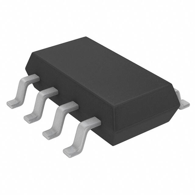
The MP3307 is available in a TSOT23-8
package, which is ideal for use in video displays.
FEATURES
2.7V to 5.5V Input Voltage
Analog Dimming with >20kHz Input Signal
Direct PWM Dimming Mode with 100Hz to
2kHz Input Signal
Up to 2.2MHz Programmable Switching
Frequency
Low 200mV Feedback Voltage with ±1%
Accuracy at Room Temperature
24V Open-Load Protection Threshold
UVLO and Thermal Shutdown
Cycle-by-Cycle Over-Current Protection
Available in a TSOT23-8 Package
APPLICATIONS
Video Displays
In-Car LCD Infotainment
Tablets
All MPS parts are lead-free, halogen-free, and adhere to the RoHS directive. For
MPS green status, please visit the MPS website under Quality Assurance.
“MPS” and “The Future of Analog IC Technology” are registered trademarks of
Monolithic Power Systems, Inc.
TYPICAL APPLICATION
95
Effi_Boost
90
85
Effi_LEDs
80
75
70
65
60
55
50
MP3307 Rev.1.0
8/25/2015
2
3
4
www.MonolithicPower.com
MPS Proprietary Information. Patent Protected. Unauthorized Photocopy and Duplication Prohibited.
© 2015 MPS. All Rights Reserved.
5
6
1
�MP3307―2.7V-5.5V INPUT, 24V OVP, –PROGRAMMABLE FSW, WHITE LED DRIVER
ORDERING INFORMATION
Part Number*
MP3307GJ
Package
TSOT23-8
Top Marking
See Below
* For Tape & Reel, add suffix –Z (e.g. MP3307GJ–Z)
TOP MARKING
ANF: Product code of MP3307GJ
Y: Year code
PACKAGE REFERENCE
TOP VIEW
TSOT23-8
ABSOLUTE MAXIMUM RATINGS (1)
Thermal Resistance
VIN ...................................................-0.3V to +6V
VSW, VOUT…………………………..…-1V to +40V
All other pins ..................................–0.3V to +6V
Junction temperature ................................150°C
Lead temperature .....................................260°C
(2)
Continuous power dissipation .....(TA = 25°C)
TSOT23-8 ................................................ 1.25W
TSOT23-8............................. 100...... 55 °C/W
Recommended Operating Conditions
(3)
Supply voltage (VIN) ........................2.7V to 5.5V
Operating junction temp. (TJ). .. -40°C to +125°C
MP3307 Rev.1.0
8/25/2015
(4)
θJA
θJC
NOTES:
1) Exceeding these ratings may damage the device.
2) The maximum allowable power dissipation is a function of the
maximum junction temperature TJ (MAX), the junction-toambient thermal resistance θJA, and the ambient temperature
TA. The maximum allowable continuous power dissipation at
any ambient temperature is calculated by PD (MAX) = (TJ
(MAX)-TA)/θJA. Exceeding the maximum allowable power
dissipation will cause an excessive die temperature, causing
the regulator to go into thermal shutdown. Internal thermal
shutdown circuitry protects the device from permanent
damage.
3) The device is not guaranteed to function outside of its
operating conditions.
4) Measured on JESD51-7, 4-layer PCB.
www.MonolithicPower.com
MPS Proprietary Information. Patent Protected. Unauthorized Photocopy and Duplication Prohibited.
© 2015 MPS. All Rights Reserved.
2
�MP3307―2.7V-5.5V INPUT, 24V OVP, –PROGRAMMABLE FSW, WHITE LED DRIVER
ELECTRICAL CHARACTERISTICS
VIN = 3.6V, VEN = VIN, TA = 25°C, unless otherwise noted.
Parameters
Symbol
Condition
Min
Typ
Max
Units
5.5
V
Step-Up Converter
Operating input voltage
VIN
Supply current (quiescent)
IQ
No load with switching
Supply current (shutdown)
IST
VEN = 0V, VIN = 3.6V
Input UVLO threshold
VIN_UVLO
2.7
440
1
Rising edge
Input UVLO hysteresis
EN high voltage
VEN_HIGH
VEN rising
EN low voltage
VEN_LOW
VEN falling
Switching frequency
fSW
Maximum duty cycle
DMAX
Feedback regulation voltage
VREF
VREF ramp-up time per step
tSTEP
μA
2.5
V
200
mV
1.2
V
0.4
ROSC = 51kΩ
μA
V
2.22
MHz
90
93
%
198
200
202
320
mV
μs
Power Switch
Main switch on resistance
RDSON_M
VIN = 3.6V
PWMH input low threshold
VPWM_LO
VPWM falling
PWMH input high threshold
VPWM_HI
VPWM rising
0.3
0.5
Ω
0.4
V
Current Dimming
PWML shutdown time
tSD
1.2
EN/PWML high to low
V
20
ms
Protection
OVP voltage
VOVP
Cycle-by-cycle current limit
OVP UVLO threshold
Thermal shutdown threshold
Thermal shutdown hysteresis
MP3307 Rev.1.0
8/25/2015
ILIM
OVP
22.5
Hysteresis
24
25.5
2
1.6
V
V
A
VOVP_UV
1.25
V
tST
150
°C
25
°C
www.MonolithicPower.com
MPS Proprietary Information. Patent Protected. Unauthorized Photocopy and Duplication Prohibited.
© 2015 MPS. All Rights Reserved.
3
�MP3307―2.7V-5.5V INPUT, 24V OVP, –PROGRAMMABLE FSW, WHITE LED DRIVER
TYPICAL PERFORMANCE CHARACTERISTICS
VIN = 3.6V, 3s*4p LEDs, L = 3.3µH, fs = 2.2MHz, TA = 25°C, unless otherwise noted.
90
90
80
80
70
70
60
60
50
50
40
40
30
30
20
20
10
10
0
MP3307 Rev.1.0
8/25/2015
0
0.2
0.4
0.6
0.8
1
0
0
0.2
0.4
0.6
0.8
www.MonolithicPower.com
MPS Proprietary Information. Patent Protected. Unauthorized Photocopy and Duplication Prohibited.
© 2015 MPS. All Rights Reserved.
1
4
�MP3307―2.7V-5.5V INPUT, 24V OVP, –PROGRAMMABLE FSW, WHITE LED DRIVER
TYPICAL PERFORMANCE CHARACTERISTICS (continued)
VIN = 3.6V, 3s*4p LEDs, L = 3.3µH, fs = 2.2MHz, TA = 25°C, unless otherwise noted.
VSW
5V/div.
VOUT
5V/div.
VSW
5V/div.
VSW
5V/div.
VOUT
2V/div.
IL
200mA/div.
ILED
100mA/div.
VOUT
2V/div.
IL
200mA/div.
ILED
100mA/div.
IL
200mA/div.
ILED
100mA/div.
VSW
5V/div.
VSW
5V/div.
VSW
5V/div.
VEN
5V/div.
VEN
5V/div.
VEN
5V/div.
IL
200mA/div.
ILED
100mA/div.
IL
200mA/div.
ILED
100mA/div.
IL
200mA/div.
ILED
100mA/div.
VSW
10V/div.
VSW
10V/div.
VOUT
20V/div.
IL
2A/div.
ILED
100mA/div.
MP3307 Rev.1.0
8/25/2015
VOUT
10V/div.
IL
2A/div.
ILED
100mA/div.
VSW
10V/div.
VOUT
5V/div.
IL
500mA/div.
ILED
100mA/div.
www.MonolithicPower.com
MPS Proprietary Information. Patent Protected. Unauthorized Photocopy and Duplication Prohibited.
© 2015 MPS. All Rights Reserved.
5
�MP3307―2.7V-5.5V INPUT, 24V OVP, –PROGRAMMABLE FSW, WHITE LED DRIVER
PIN FUNCTIONS
Pin #
1
2
3
4
5
6
7
8
MP3307 Rev.1.0
8/25/2015
Name
Description
Power switch node. SW is the drain of the internal low-side MOSFET. Connect the
SW
power inductor between SW and VIN.
OVP
Over-voltage sensing.
GND
Ground.
LED current feedback. FB regulates the voltage across the current-sense resistor
FB
between FB and GND to 200mV.
Switching frequency set. Connect a resistor between FREQ and GND to program
FREQ
the converter switching frequency. Do NOT leave FREQ floating.
PWM brightness control/enable. Apply a PWM signal for PWM dimming. The PWM
frequency is proportional to the LED current dimming ratio—a lower dimming
EN/PWML
frequency results in a smaller dimming current. For most applications, use a frequency
range of 200Hz to 2kHz. A low-level signal longer than 20ms will shut down the IC.
Analog dimming input. A >20kHz PWM signal is recommended if a PWM signal input
PWMH
is being used for analog dimming.
Input supply. VIN provides power for internal power and the logic circuits. VIN must
VIN
be bypassed locally.
www.MonolithicPower.com
MPS Proprietary Information. Patent Protected. Unauthorized Photocopy and Duplication Prohibited.
© 2015 MPS. All Rights Reserved.
6
�MP3307―2.7V-5.5V INPUT, 24V OVP, –PROGRAMMABLE FSW, WHITE LED DRIVER
Figure 1: Functional Block Diagram
MP3307 Rev.1.0
8/25/2015
www.MonolithicPower.com
MPS Proprietary Information. Patent Protected. Unauthorized Photocopy and Duplication Prohibited.
© 2015 MPS. All Rights Reserved.
7
�MP3307―2.7V-5.5V INPUT, 24V OVP, –PROGRAMMABLE FSW, WHITE LED DRIVER
OPERATION
The MP3307 uses peak-current-mode control to
regulate the current through the WLED string.
At the start of each oscillator cycle, the control
circuit turns on the low-side MOSFET (LS-FET,
M1). A stabilizing ramp is added to the output of
the current sense amplifier, which feeds into the
positive input of the PWM comparator and
prevents sub-harmonic oscillations at duty
cycles greater than 50%. When the input of the
PWM comparator equals the output voltage of
the error amplifier, M1 turns off. The inductor
current then flows through the external Schottky
diode, which forces the inductor current to
decrease.
The voltage at the output of the error amplifier
is the amplified difference between the 200mV
reference voltage and the feedback voltage. If
the feedback voltage starts to drop, the output
of the error amplifier increases. This also
increases the current flowing through M1, the
power to the inductor, and the output power.
This method regulates the LED current
accurately.
System Start-Up
When enabled, the MP3307 checks safety
limits, including UVLO, over-temperature
protection (OTP), and over-current protection
(OCP). If all of the protection tests pass, the
chip then boosts the step-up converter with an
internal soft start. During the soft start, the
current reference increases from 0 to 200mV in
32 steps (320µs per step) to prevent a large
inrush current.
Dimming Control
The MP3307 provides two dimming methods:
PWM dimming and analog dimming mode.
For PWM dimming, apply a PWM signal to
EN/PWML. The LED current is then segmented
according to the PWM signal and the average
LED current. See Equation (1):
Iset D dim
When the PWM signal is high, the converter
operates in normal mode. Conversely, when the
PWM amplitude is low, the converter stops
switching. If the PWM signal low-level time is
more than 20ms, the IC shuts down. Use a
100Hz to 2kHz PWM dimming frequency for
most dimming ratio requests.
For analog dimming, connect the PWM
dimming signal to PWMH. An internal RC filter
filters the PWM signal. The LED current
amplitude equals Iset×Ddim, where Ddim is the
PWM duty cycle, and Iset is the LED current
amplitude. Use a >20kHz PWM signal to
improve filtering performance.
Open-String Protection
The MP3307 monitors VOUT for open-string
protection. If the LED string is open, the
feedback voltage is lower than the reference
voltage. The COMP then rises and charges the
output capacitor until the VOUT reaches the
protection point (VOVP).
The IC stops switching when VOUT reaches the
OVP threshold; it resumes operation when VOUT
drops below the threshold.
Input Under-Voltage Protection
When VIN exceeds 2.5V, the converter starts to
charge the internal reference and provides
power to the internal control circuitry. There is
an UVLO hysteresis (approximately 200mV) as
VIN falls. The IC shuts down when the input
voltage drops below 2.3V.
Thermal Shutdown Protection
Thermal shutdown prevents the IC from
operating at exceedingly high temperatures.
When the die temperature exceeds the upper
threshold (TST), the IC shuts down; it resumes
normal operation when the die temperature
drops below the lower threshold. Typically, the
hysteresis is 25°C.
(1)
Where Ddim is the PWM duty cycle, and Iset is the
LED current amplitude.
MP3307 Rev.1.0
8/25/2015
www.MonolithicPower.com
MPS Proprietary Information. Patent Protected. Unauthorized Photocopy and Duplication Prohibited.
© 2015 MPS. All Rights Reserved.
8
�MP3307―2.7V-5.5V INPUT, 24V OVP, –PROGRAMMABLE FSW, WHITE LED DRIVER
APPLICATION INFORMATION
Selecting the Switching Frequency
The switching frequency of the step-up
converter can be programmed from 300kHz to
1.2MHz. A resistor on OSC sets the internal
oscillator frequency for the step-up converter
with Equation (2):
fSW (kHz)
120000
ROSC (k )
(2)
For instance, if ROSC=51kΩ, then the switching
frequency is 2.35MHz.
Setting the LED Current
Set the LED current through the current-setting
resistor on FB using Equation (3):
ILED (mA)
VREF (V)
1000
RFB ( )
(3)
For instance, if VREF=200mV, and RFB=10Ω,
then the LED current is 20mA. Do NOT leave
FB floating.
Selecting the Input Capacitor
The input capacitor reduces the surge current
drawn from the input supply and the switching
noise from the device. The input capacitor
impedance at the switching frequency should
be less than the input source impedance to
prevent the high-frequency switching current
from passing through to the input. Use ceramic
capacitors with X5R or X7R dielectrics for their
low ESR and small temperature coefficients.
For most applications, use a 2.2µF to 10μF
ceramic capacitor.
Selecting the Inductor
The MP3307 requires an inductor to boost its
output voltage. An inductor with a larger value
results in less ripple current; it also lowers both
the peak inductor current and stress on the
internal N-channel MOSFET. However, the
larger inductor is physically larger and has both
a higher series resistance and a lower
saturation current.
Choose an inductor that does not saturate
under the worst-case load conditions. Select a
minimum inductor value to ensure that the
boost converter works in continuous conduction
MP3307 Rev.1.0
8/25/2015
mode with high efficiency and good EMI
performance.
Calculate the required inductance value using
Equation (4) and Equation (5):
η VOUT D (1 D)2
L
(4)
2 fSW ILOAD
V
(5)
D 1 IN
VOUT
Where VIN and VOUT are the input and output
voltages, fSW is the switching frequency, ILOAD is
the LED load current, and η is the efficiency.
To avoid hitting the switching current limit for
peak current mode, the worst-case inductor
peak current should be less than 80% of the
current limit (ILIM).
Selecting the Output Capacitor
The output capacitor keeps the output voltage
ripple small and ensures feedback loop stability.
The output capacitor impedance must be low at
the switching frequency. Ceramic capacitors
with X7R dielectrics are recommended for their
low ESR characteristics. Selection must also
account for the capacitance’s dependence on
the voltage rating. With DC bias voltage, the
capacitor can lose as much as 50% of its
capacitance at its rated voltage rating. Leave a
sufficient voltage rating margin when selecting
the component.
A capacitance that is too low or too high causes
loop instability. For most applications, select a
capacitor in the range of 2.2µF to 10μF.
PCB Layout Guidelines
Efficient PCB layout is critical for preventing
noise, limiting electromagnetic interference, and
achieving stable operation. For best results,
refer to Figure 2 and follow the guidelines below:
1. Minimize the loop consisting of the
MP3307’s internal low-side MOSFET,
external Schottky diode, and output
capacitor, as it contains a highfrequency ripple current.
2. Place the input and output capacitors as
close to the IC as possible.
www.MonolithicPower.com
MPS Proprietary Information. Patent Protected. Unauthorized Photocopy and Duplication Prohibited.
© 2015 MPS. All Rights Reserved.
9
�MP3307―2.7V-5.5V INPUT, 24V OVP, fs-PROGRAMMABLE, WHITE LED DRIVER
TYPICAL APPLICATION CIRCUITS
L1
3.3µH
VIN
D1
C1
4.7µF/10V
GND
C2
4.7µF
/25V
SW
OVP
IN
MP3307
PWMH
3s*Np
PWMH
EN/PWML
PWM
FREQ
R2
51kΩ
FB
GND
Rs
Figure 2: Typical Application for 3s*Np LEDs
MP3307 Rev.1.0
8/25/2015
www.MonolithicPower.com
MPS Proprietary Information. Patent Protected. Unauthorized Photocopy and Duplication Prohibited.
© 2015 MPS. All Rights Reserved.
10
�MP3307―2.7V-5.5V INPUT, 24V OVP, fs-PROGRAMMABLE, WHITE LED DRIVER
PACKAGE INFORMATION
TSOT23-8
See note 7
EXAMPLE TOP
MARK
PIN 1 ID
IAAAA
RECOMMENDED LAND PATTERN
TOP VIEW
SEATING PLANE
SEE DETAIL ''A''
FRONT VIEW
SIDE VIEW
NOTE:
DETAIL ''A''
NOTICE: The information in this document is subject to change without notice. Please contact MPS for current specifications.
Users should warrant and guarantee that third party Intellectual Property rights are not infringed upon when integrating MPS
products into any application. MPS will not assume any legal responsibility for any said applications.
MP3307 Rev. 1.0
8/25/2015
www.MonolithicPower.com
MPS Proprietary Information. Patent Protected. Unauthorized Photocopy and Duplication Prohibited.
© 2015 MPS. All Rights Reserved.
11
�