MP3309A
2.7V-5.5V Input, 35V Output,
Programmable Fsw, White LED Driver
The Future of Analog IC Technology
DESCRIPTION
The MP3309A is a WLED step-up converter for
2.7V-to-5.5V input that uses peak-current mode
to regulate the LED current sensed through an
external low-side resistor. The 200mV feedback
voltage and synchronous rectification reduces
power loss and reduces PCB space
requirements. To connect an external Schottky
accomplishes the non-synchronous mode for
heavy load to improve the thermal performance.
The MP3309A features a programmable
switching frequency to optimize efficiency. It
supports both analog and PWM dimming.
In addition, the MP3309A has LED open
protection,
cycle-by-cycle
current
limit
protection, thermal shutdown protection and
over-voltage protection. MP3309A is available
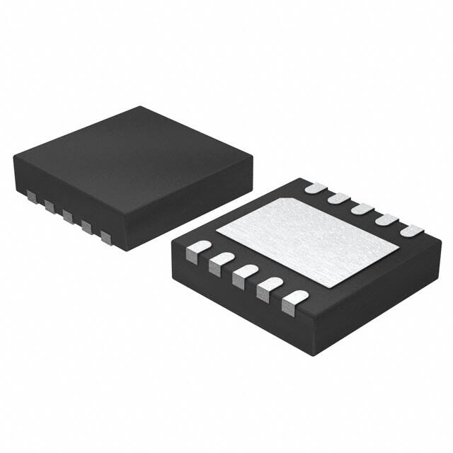
in QFN10 3*3mm package.
FEATURES
•
•
•
•
•
•
•
•
•
2.7V-to-5.5V Input Voltage
Low 200mV Feedback Voltage with ±1%
Accuracy
Synchronous Mode
Analog and PWM Dimming
Programmable Switching Frequency
35.5V Over Voltage Protection Point
Hardware-Enable Function
UVLO, Thermal Shutdown
Available in 3x3mm QFN10 Package
APPLICATIONS
•
•
•
Feature Phones and Smart Phones
Tablets
Video Displays
All MPS parts are lead-free and adhere to the RoHS directive. For MPS green
status, please visit MPS website under Products, Quality Assurance page.
“MPS” and “The Future of Analog IC Technology” are Registered Trademarks of
Monolithic Power Systems, Inc.
TYPICAL APPLICATION
MP3309A Rev. 1.11
www.MonolithicPower.com
1/15/2016
MPS Proprietary Information. Patent Protected. Unauthorized Photocopy and Duplication Prohibited.
© 2016 MPS. All Rights Reserved.
1
�MP3309A 2.7V-5.5V INPUT, 35V OUTPUT, PROGRAMMABLE FSW, WHITE LED DRIVER
ORDERING INFORMATION
Part Number
MP3309AGQ*
Package
QFN10 (3x3mm)
Top Marking
AJFY
* For Tape & Reel, add suffix –Z (e.g. MP3309AGQ–Z);
PACKAGE REFERENCE
TOP VIEW
TOP VIEW
VOUT
1
10
BST
SW
2
9
PWMH
GND
3
8
PWMH
FB
4
7
VIN
FREQ
5
6
EN/PWML
QFN10 (3x3mm)
ABSOLUTE MAXIMUM RATINGS (1)
Thermal Resistance
VIN ...................................................-0.3V to +6V
VSW, VOUT…………………………..…-1V to +40V
VBST ......................................... -0.3V to VSW +6V
All Other Pins .................................–0.3V to +6V
Junction Temperature ...............................150°C
Lead Temperature ....................................260°C
(2)
Continuous Power Dissipation ....(TA = 25°C)
QFN10(3x3mm) ......................................... 2.5W
QFN10 (3×3mm).................... 50....... 12 °C/W
Recommended Operating Conditions
(3)
Supply Voltage VIN ..........................2.7V to 5.5V
Operating Junction Temp. (TJ). -40°C to +125°C
(4)
θJA
θJC
Notes:
1) Exceeding these ratings may damage the device.
2) The maximum allowable power dissipation is a function of the
maximum junction temperature TJ (MAX), the junction-toambient thermal resistance θJA, and the ambient temperature
TA. The maximum allowable continuous power dissipation at
any ambient temperature is calculated by PD (MAX) = (TJ
(MAX)-TA)/θJA. Exceeding the maximum allowable power
dissipation will cause excessive die temperature, and the
regulator will go into thermal shutdown. Internal thermal
shutdown circuitry protects the device from permanent
damage.
3) The device is not guaranteed to function outside of its
operating conditions.
4) Measured on JESD51-7, 4-layer PCB.
MP3309A Rev. 1.11
www.MonolithicPower.com
1/15/2016
MPS Proprietary Information. Patent Protected. Unauthorized Photocopy and Duplication Prohibited.
© 2016 MPS. All Rights Reserved.
2
�MP3309A 2.7V-5.5V INPUT, 35V OUTPUT, PROGRAMMABLE FSW, WHITE LED DRIVER
ELECTRICAL CHARACTERISTICS
VIN =3.6V, VEN = VIN, TA = 25°C, unless otherwise noted.
Parameters
Symbol
Condition
Min
Typ
Max
Units
5.5
V
STEP-UP CONVERTER
Operating Input Voltage
VIN
2.7
Supply Current (Quiescent)
IQ
VIN=3.6V, VEN= VIN, no
load with switching
Supply Current (Shutdown)
IST
VEN=0V, VIN=3.6V
Input UVLO Threshold
VIN_UVLO
420
1
Rising Edge
Input UVLO Hysteresis
EN High Voltage
VEN_HIGH
VEN Rising
EN Low Voltage
VEN_LOW
VEN Falling
Switching Frequency
fSW
Maximum Duty Cycle
DMAX
Feedback Regulation Voltage
VREF
μA
μA
2.5
V
200
mV
1.2
V
0.4
V
740
kHz
RFREQ= 200kΩ
540
640
Sync Mode, 640kHz
89
93
198
200
202
mV
%
POWER SWITCH
Main Switch On-Resistance
RDSON_M
VIN=3.6V
0.3
0.5
Ω
Sync Switch On-Resistance
RDSON_S
VIN=3.6V
0.5
0.8
Ω
PWMH Input Low Threshold
VPWM_LO
VPWM Falling
0.4
V
PWMH Input High Threshold
VPWM_HI
VPWM Rising
CURRENT DIMMING
PWML Shutdown Time
tSD
1.2
EN/PWML High to Low
V
20
ms
PROTECTION
OVP Voltage
Cycle-Cycle Current Limit
VOVP
33.5
Hysteresis
37.5
V
2.5
V
1.8
A
0.8
A
ILIM
Max Duty Cycle
Startup Current Limit
ILIM_START
Max Duty Cycle
Time Step for Half Current Limit
TLIM_HALF
5
ms
OVP UVLO Threshold
VOVP_UV
1.24
V
tST
150
°C
25
°C
Thermal Shutdown Threshold
Thermal Shutdown Hysteresis
1.4
35.5
MP3309A Rev. 1.11
www.MonolithicPower.com
1/15/2016
MPS Proprietary Information. Patent Protected. Unauthorized Photocopy and Duplication Prohibited.
© 2016 MPS. All Rights Reserved.
3
�MP3309A 2.7V-5.5V INPUT, 35V OUTPUT, PROGRAMMABLE FSW, WHITE LED DRIVER
TYPICAL PERFORMANCE CHARACTERISTICS
440
35.54
2.530
435
35.52
2.528
35.50
2.526
35.48
2.524
35.46
2.522
35.44
2.520
405
35.42
2.518
400
35.40
2.516
395
-60 -40 -20 0 20 40 60 80100120140
35.38
-60 -40 -20 0 20 40 60 80100120140
2.514
-60 -40 -20 0 20 40 60 80100120140
430
425
420
415
410
642
2400
200.2
640
2200
200.0
638
636
634
2000
1800
199.8
199.6
1600
1400
199.4
632
1200
199.2
630
-60 -40 -20 0 20 40 60 80100120140
1000
-60 -40 -20 0 20 40 60 80100120140
199.0
-60 -40 -20 0 20 40 60 80100120140
MP3309A Rev. 1.11
www.MonolithicPower.com
1/15/2016
MPS Proprietary Information. Patent Protected. Unauthorized Photocopy and Duplication Prohibited.
© 2016 MPS. All Rights Reserved.
4
�MP3309A 2.7V-5.5V INPUT, 35V OUTPUT, PROGRAMMABLE FSW, WHITE LED DRIVER
TYPICAL PERFORMANCE CHARACTERISTICS (continued)
VIN = 3.6V, 8 LEDs, L = 10µH(59mΩ) ILED=80mA, TA = 25°C, unless otherwise noted.
100
95
90
VSW
10V/div.
85
80
75
70
65
60
2.8
VSW
10V/div.
VEN
5V/div.
ILED
50mA/div.
IL
500mA/div.
3.3
3.8
4.3
VSW
10V/div.
VIN
2V/div.
VIN
2V/div.
ILED
50mA/div.
ILED
50mA/div.
IL
500mA/div.
IL
500mA/div.
VSW
20V/div.
VSW
20V/div.
VPWML
5V/div.
VPWMH
5V/div.
ILED
50mA/div.
IL
500mA/div.
ILED
50mA/div.
IL
500mA/div.
VSW
10V/div.
ILED
50mA/div.
VOUT
10V/div.
MP3309A Rev. 1.11
www.MonolithicPower.com
1/15/2016
MPS Proprietary Information. Patent Protected. Unauthorized Photocopy and Duplication Prohibited.
© 2016 MPS. All Rights Reserved.
5
�MP3309A 2.7V-5.5V INPUT, 35V OUTPUT, PROGRAMMABLE FSW, WHITE LED DRIVER
PIN FUNCTIONS
Pin #
1
2
3
4
5
6
7
8,9
10
Name
Description
Output Voltage. For non-synchronous mode, connect a Schottky diode between SW pin
VOUT
and this pin.
Power Switch Node. Drain of the internal low-side MOSFET. Connect the power inductor
SW
between SW and VIN pin. For non-synchronous mode, connect a Schottky diode
between this pin and VOUT.
GND
Ground.
LED Current Feedback. Regulates the voltage across the current sense resistor between
FB
FB and GND to 200mV.
Switching Frequency Set. Connect a resistor between this pin and GND to program the
FREQ
converter switching frequency. Do not leave this pin floating.
Enable and PWM Brightness Control Pin. Apply a PWM signal for PWM dimming. For
EN/PWML most applications, use a frequency range of 200Hz to 2kHz. A low-level signal longer
than 20ms will shutdown the IC.
Input Supply Pin. Provides power for internal power and logic circuits. Must be locally
VIN
bypassed.
Dimming input pin for PWM input analog dimming, >20kHz PWM signal is
PWMH
recommended. Pull 2 pins high together when analog dimming is not used.
Bootstrap. Connect a capacitor between SW and BST pin to provide the synchronous
BST
MOSFET gate driver.
MP3309A Rev. 1.11
www.MonolithicPower.com
1/15/2016
MPS Proprietary Information. Patent Protected. Unauthorized Photocopy and Duplication Prohibited.
© 2016 MPS. All Rights Reserved.
6
�MP3309A 2.7V-5.5V INPUT, 35V OUTPUT, PROGRAMMABLE FSW, WHITE LED DRIVER
FUNCTION BLOCK DIAGRAM
BG&Logic
Control Unit
EN
Detect
EN/PWML
M2
Regulator
OSC
VREF&DPWM
PWM
Control
RAMP
M1
DPWM
VREF
EA
PWM
Comparator
OSC
Figure 1: Functional Block Diagram
MP3309A Rev. 1.11
www.MonolithicPower.com
1/15/2016
MPS Proprietary Information. Patent Protected. Unauthorized Photocopy and Duplication Prohibited.
© 2016 MPS. All Rights Reserved.
7
�MP3309A 2.7V-5.5V INPUT, 35V OUTPUT, PROGRAMMABLE FSW, WHITE LED DRIVER
OPERATION
The MP3309A uses peak-current-mode control to
regulate the current through the WLED string. At
the start of each oscillator cycle, the control
circuit turns on the low-side MOSFET (LS-FET,
M1). A stabilizing ramp added to the output of the
current-sense amplifier, which then feeds into the
positive input of the PWM comparator, prevents
sub-harmonic oscillations at duty cycles greater
than 50%. When the input of the PWM
comparator is equal to the output voltage of the
error amplifier, M1 turns off. Then the inductor
current flows through the synchronous power
MOSFET, which forces the inductor current to
decrease.
The voltage at the output of the error amplifier is
the amplified difference between the 200mV
reference voltage and the feedback voltage. If
the feedback voltage starts to drop, the output of
the error amplifier increases, increasing the
current flowing through the M1, thus increasing
the power to the inductor and output power. This
method accurately regulates the LED current.
System Startup
When enabled, the MP3309A checks safety
limits, including UVLO and over-temperature
protection (OTP), over-current protection after
passing the OVP test. If all the protection tests
pass, the chip then starts boosting the step-up
converter with an internal soft-start. During the
soft-start, the current limit drops to 0.8A to
prevent a large inrush current. This low-currentlimit time lasts for 5ms after the IC is enabled.
Synchronous Mode
The converter works in synchronous mode.
Synchronous mode can reduce diode power
consumption caused by a large voltage drop.
This synchronous mode increases the converter
efficiency for low LED string voltage. This mode
does not need an external Schottky diode,
reducing PCB space requirements and BOM
costs.
Dimming Control
The MP3309A provides two dimming methods:
PWM and analog dimming.
segmented as per the PWM signal and the
average LED current equals:
Iset × D dim
Where Ddim is the PWM duty cycle and Iset is the
LED current amplitude. When PWM signal is high,
the converter operates in normal mode.
Conversely, when the PWM amplitude is low, the
converter stops switching. Make sure that the
PWM-signal low-level time is less than 20ms,
otherwise the IC will shutdown. Use a 100Hz-to2kHz PWM-dimming frequency for most dimming
ratio requests.
For analog dimming, set the LED current
amplitude through an external PWM signal.
Implementing analog dimming by connecting the
2 PWMH pins together and apply a PWM signal.
An internal RC filter filters the PWM signal. The
LED current amplitude equals Iset×Ddim, where
Ddim is the PWM duty cycle and Iset is the LED
current amplitude. Use a >20kHz PWM signal to
improve filtering performance.
IC Enable and Shutdown
The MP3309A enables the internal band-gap and
normal switching when the EN/PWML pin is high.
The MP3309A shuts down the chip when the
EN/PWML pin is low for longer than 20ms.
Open-String Protection
The MP3309A monitors the VOUT pin for openstring protection. If the LED string is open, the
feedback voltage is lower than the reference
voltage. The COMP then rises and charges the
output capacitor until the VOUT voltage reaches
the protection point VOVP(35.5V).
The IC stops switching when VOUT reaches the
OVP threshold, the IC resumes function when
VOUT drops below the threshold.
Input Under-Voltage Protection
When VIN exceeds 2.5V, the converter starts to
charge the internal reference and provides power
to the internal control circuitry. There is UVLO
hysteresis, approximately 200mV, as VIN falls.
The IC shuts down when the input voltage drops
below 2.3V.
For PWM dimming, apply a PWM signal to the
EN/PWML pin. The LED current is then
MP3309A Rev. 1.11
www.MonolithicPower.com
1/15/2016
MPS Proprietary Information. Patent Protected. Unauthorized Photocopy and Duplication Prohibited.
© 2016 MPS. All Rights Reserved.
8
�MP3309A 2.7V-5.5V INPUT, 35V OUTPUT, PROGRAMMABLE FSW, WHITE LED DRIVER
Thermal-Shutdown Protection
Thermal shutdown prevents the IC from
operating at exceedingly high temperatures.
When the die temperature exceeds the upper
threshold (TST), the IC shutdowns and resumes
normal operation when the die temperature drops
below lower threshold. Typically, the hysteresis is
25°C.
MP3309A Rev. 1.11
www.MonolithicPower.com
1/15/2016
MPS Proprietary Information. Patent Protected. Unauthorized Photocopy and Duplication Prohibited.
© 2016 MPS. All Rights Reserved.
9
�MP3309A 2.7V-5.5V INPUT, 35V OUTPUT, PROGRAMMABLE FSW, WHITE LED DRIVER
APPLICATION INFORMATION
Selecting the Switching Frequency
The switching frequency of the step-up converter
can be programmed from 300kHz to 1.2MHz. A
resistor on the FREQ pin sets the internal
oscillator frequency for the step-up converter as
per the equation below:
FSW (KHz ) =
128000
RFREQ (KΩ )
For instance, if RFREQ=200kΩ, the switching
frequency is to 640kHz.
Calculate the required inductance value using the
equation:
η × VOUT × D × (1− D)2
L≥
2 × fSW × ILOAD
V
D = 1 − IN
VOUT
Where VIN and VOUT are the input and output
voltages, fSW is the switching frequency, ILOAD is
the LED load current, and η is the efficiency.
To avoid hitting the current limit, the worst-case
inductor peak current should be less than 80% of
the current limit, ILIM.
Setting the LED Current
Set the LED current through the current-setting
resistor on the FB pin.
ILED (mA) =
VREF (V)
× 1000
RFB (Ω)
For instance, if VREF=200mV, and RFB=10Ω, the
LED current is 20mA. Do not leave the FB pin
floating.
Selecting the Input Capacitor
The input capacitor reduces the surge current
drawn from the input supply and the switching
noise from the device. The input capacitor
impedance at the switching frequency should be
less than the input source impedance to prevent
the high-frequency switching current from
passing through to the input. Use ceramic
capacitors with X5R or X7R dielectrics for their
low ESR and small temperature coefficients. For
most applications, use a 2.2µF-to-10μF ceramic
capacitor.
Selecting the Inductor
The MP3309A requires an inductor to boost its
output voltage. A larger value inductor results in
less ripple current, lowering both the peakinductor current and the stress on the internal Nchannel MOSFET. However, the larger inductor
is physically larger, has a higher series
resistance, and a lower saturation current.
Choose an inductor that does not saturate under
the worst-case load conditions. Select the
minimum inductor value to ensure that the boost
converter works in continuous-conduction mode
with high efficiency and good EMI performance.
IL(PEAK) =
VOUT × ILOAD VIN × (VOUT − VIN )
+
ηVIN
2 × L × fSW × VOUT
Where IL(PEAK) is the inductor peak current.
Selecting the Output Capacitor
The output capacitor keeps the output voltage
ripple small and ensures feedback loop stability.
The output capacitor impedance must be low at
the switching frequency. Ceramic capacitors with
X7R dielectrics are recommended for their low
ESR characteristics. Selection must also account
for the capacitance’s dependence on the voltage
rating; with a DC bias voltage, the capacitor can
lose as much as 50% of its capacitance at its
rated voltage rating. Leave a sufficient voltage
rating margin when select the component.
For most applications, select a capacitor in the
range of 0.33µF to 3.3μF.
Setting the Over-Voltage Protection Point
VOUT determines the OVP point for open-string
protection. In some cases, an LED string failure
results in a 0V feedback voltage. The part then
continuously boosts the output voltage higher
and higher until the output voltage reaches the
programmed OVP threshold to trigger openstring protection.
Dimming Mode
The MP3309A has a smart dimming function for
both PWM and analog dimming.
1.
For PWM dimming, apply a 100Hz-to-2kHz
PWM signal to the EN/PWML pin. Make sure
that the PWM-signal low-level time is less
than 20ms, otherwise the IC will shutdown.
MP3309A Rev. 1.11
www.MonolithicPower.com
1/15/2016
MPS Proprietary Information. Patent Protected. Unauthorized Photocopy and Duplication Prohibited.
© 2016 MPS. All Rights Reserved.
10
�MP3309A 2.7V-5.5V INPUT, 35V OUTPUT, PROGRAMMABLE FSW, WHITE LED DRIVER
2.
For analog dimming, set the LED current
amplitude through an external >20kHz PWM
signal on 2 PWMH pins.
Layout Considerations
Careful attention must be paid to the PCB board
layout and components placement.
Proper layout of the high frequency switching
path is critical to prevent noise and limit
electromagnetic interference. The loop consisting
of MP3309A’s internal low-side MOSFET,
synchronous MOSFET or diode, and output
capacitor contains a high-frequency ripple
current—minimize this loop. Place the output
capacitor should as to the IC as possible.
MP3309A Rev. 1.11
www.MonolithicPower.com
1/15/2016
MPS Proprietary Information. Patent Protected. Unauthorized Photocopy and Duplication Prohibited.
© 2016 MPS. All Rights Reserved.
11
�MP3309A 2.7V-5.5V INPUT, 35V OUTPUT, PROGRAMMABLE FSW, WHITE LED DRIVER
TYPICAL APPLICATION CIRCUITS
L1
22μH
VIN
R3
0Ω
C1
4.7μF/10V
C2
10nF
GND
SW
IN
BST
OUT
MP3309A
PWMH
PWMH
PWMH
EN/PWML
C3
0.47μF
/50V
8*LEDs
EN/PWM
FREQ
R2
100k
GND
FB
R1
10Ω
Figure 2: Typical Application for Single String 8LEDs (Synchronous)
MP3309A Rev. 1.11
www.MonolithicPower.com
1/15/2016
MPS Proprietary Information. Patent Protected. Unauthorized Photocopy and Duplication Prohibited.
© 2016 MPS. All Rights Reserved.
12
�MP3309A 2.7V-5.5V INPUT, 35V OUTPUT, PROGRAMMABLE FSW, WHITE LED DRIVER
PACKAGE INFORMATION
QFN10 (3x3mm)
2.90
3.10
0.30
0.50
PIN 1 ID
MARKING
0.18
0.30
2.90
3.10
PIN 1 ID
INDEX AREA
1.45
1.75
PIN 1 ID
SEE DETAIL A
10
1
2.25
2.55
0.50
BSC
5
6
TOP VIEW
BOTTOM VIEW
PIN 1 ID OPTION A
R0.20 TYP.
PIN 1 ID OPTION B
R0.20 TYP.
0.80
1.00
0.20 REF
0.00
0.05
SIDE VIEW
DETAIL A
NOTE:
2.90
0.70
1) ALL DIMENSIONS ARE IN MILLIMETERS.
2) EXPOSED PADDLE SIZE DOES NOT INCLUDE MOLD FLASH.
3) LEAD COPLANARITY SHALL BE 0.10 MILLIMETER MAX.
4) DRAWING CONFORMS TO JEDEC MO-229, VARIATION VEED-5.
5) DRAWING IS NOT TO SCALE.
1.70
0.25
2.50
0.50
RECOMMENDED LAND PATTERN
NOTICE: The information in this document is subject to change without notice. Please contact MPS for current specifications.
Users should warrant and guarantee that third party Intellectual Property rights are not infringed upon when integrating MPS
products into any application. MPS will not assume any legal responsibility for any said applications.
MP3309A Rev. 1.11
www.MonolithicPower.com
1/15/2016
MPS Proprietary Information. Patent Protected. Unauthorized Photocopy and Duplication Prohibited.
© 2016 MPS. All Rights Reserved.
13
�