MP3351
60V, 2A Integrated Photo Flash Charger
With IGBT Driver
The Future of Analog IC Technology
DESCRIPTION
FEATURES
The MP3351 is a fast, highly efficient, precision
high voltage photo-flash charger with integrated
IGBT driver for xenon flash applications. The
programmable peak current from 300mA to 2A.
A 200mΩ internal power switch minimizes the
conduction loss. 60V maximum output voltage
lowers the transformer turns ratio and improves
switching loss associated with the primary
leakage inductance. External feedback provides
3% charge accuracy.
•
•
•
•
•
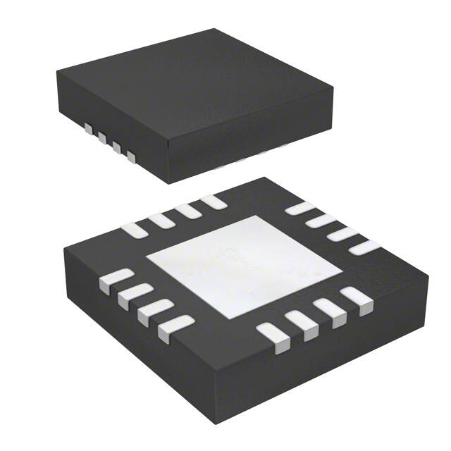
The MP3351 is available in a 16-pin 3mm x
3mm QFN package
Integrated 60V, 200mΩ Power Switch
Operates from a Single or Duel-Cell Li+ Battery
2A peak current w/resistor program
3% Charge Accuracy
Integrated IGBT Driver
APPLICATIONS
•
•
•
•
Digital Still Cameras
Optical Film Cameras
Mobile Phones With Camera
PDAs With Camera
“MPS” and “The Future of Analog IC Technology” are Registered Trademarks
of Monolithic Power Systems, Inc.
TYPICAL APPLICATION
T1
VBATT
1.3V-9V
Single or Dual Cell Battery
VOUT
+
-
3-6V
VIN
ISET
1
3, 6
SW
12, 13
7, 8
RDYB
PGND
15
2, 4
GND
MP3351
IGBTIN
14
16
9
10, 11
N/C
MP3351 Rev. 0.91
9/2/2008
FB
IGBT
CHARGE
5
IGBTOUT
www.MonolithicPower.com
MPS Proprietary Information. Unauthorized Photocopy and Duplication Prohibited.
© 2008 MPS. All Rights Reserved.
1
�MP3351 – 60V, 2A INTEGRATED PHOTO FLASH CHARGER WITH IGBT DRIVER
ABSOLUTE MAXIMUM RATINGS (1)
PACKAGE REFERENCE
16
15
14
13
1
12
2
11
3
10
4
9
5
6
7
VIN to GND ........................................ -0.3V to 6V
CHARGE, ISET, IGBTIN, RDYB to GND..-0.3V to 6V
FB to GND ........................................ -0.3V to 6V
SW to GND ..................................... -0.3V to 60V
Maximum Operating Frequency .............400kHz
Operating Temperature Ranges ....-40°C to +85°C
Storage Temperature ...............-55°C to +150°C
Junction Temperature.............................+150°C
Lead Temperature (Solder) ....................+260°C
Thermal Resistance
(2)
θJA
θJC
QFN16 (3mm x 3mm) ............. 50 ...... 12... °C/W
8
Notes:
1) Exceeding these ratings may damage the device.
2) Measured on approximately 1” square of 1 oz copper.
Part Number*
Package
Temperature
MP3351DQ
QFN16-3
–40°C to +85°C
*
For Tape & Reel, add suffix –Z (eg. MP3351DQ–Z)
For RoHS compliant packaging, add suffix –LF (eg.
MP3351DQ–LF–Z)
ELECTRICAL CHARACTERISTICS
(VIN=V (CHARGE)=3.3V, TA = +25°C, unless otherwise noted.)
Parameter
Photoflash Capacitor Charger
VIN Voltage Range
VIN UVLO
VIN Quiescent Current
VIN Quiescent Current
Shutdown Current from VIN
VSW Leakage Current
SW ON resistance between SW
and GND
Charge Input High Voltage
Charge Input Low Voltage
Pull-down resistance of
CHARGE pin
IPEAK1
IPEAK2
Charge completion detect
voltage at FB
FB input bias current I(FB)
DCM Comparator threshold
MP3351 Rev. 0.91
9/2/2008
Conditions
Rising edge, hysteresis = 200mV
V(CHARGE)=High, V(SW) = 0, free
run by TONMAX
V(CHARGE)=High, V(FB) = 1.3V
V(CHARGE)=Low, VIN =3.3V
VIN=3.3V,VSW=60V, in Shutdown
Min
3
2.7
Typ
Max
Unit
2.8
6
2.9
V
V
2.5
5
mA
1
2
µA
µA
µA
50
Switch turn-on
0.2
Ω
2.4
0.6
V(CHARGE)=3.3V
RSET=43.1kΩ
RSET=100kΩ
With 1.2KΩ (1%) connected to FB
100
V
V
kΩ
1.08
0.3
1.20
0.5
1.32
0.7
A
A
1.176
1.20
1.224
V
25
0.2
35
µA
mV
-0.2
15
www.MonolithicPower.com
MPS Proprietary Information. Unauthorized Photocopy and Duplication Prohibited.
© 2008 MPS. All Rights Reserved.
2
�MP3351 – 60V, 2A INTEGRATED PHOTO FLASH CHARGER WITH IGBT DRIVER
ELECTRICAL CHARACTERISTICS (continued)
(VIN=V (CHARGE)=3.3V, TA = +25°C, unless otherwise noted.)
Parameter
Conditions
RDYB Leakage Current
V(RDYB)=3.3V
RDYB Output Low Voltage
ISINK= 2mA
MAX TON
Maximum TON time
Thermal Shutdown
IGBT Driver
IGBTOUT pull-up ON resistance
Rising edge, Hysteresis = 15oC
Min
Max
Unit
1
µA
0.2
50
80
V
120
C
4
Ω
4
Ω
2.4
V
IGBTIN Input Low Voltage
0.6
Propagation delay
µs
o
150
IGBTOUT pull-down ON
resistance
IGBTIN Input High Voltage
Typ
V
IGBTIN rising/falling edge to
IGBTOUT rising/falling edge,
CGATE=6500pF
45
ns
IGBTOUT rise time
CGATE=6500pF
60
ns
IGBTOUT fall time
CGATE=6500pF
70
ns
100K
Ω
Pull down resistance of IGBTIN
PIN FUNCTIONS
Pin#
1
2, 4
Name
ISET
GND
3, 6
VIN
5
IGBTOUT
PGND,
Exposed Pad
7, 8
9
CHARGE
12, 13
14
SW
IGBTIN
15
RDYB
16
FB
MP3351 Rev. 0.91
9/2/2008
Description
Peak Current Set Input. The peak current is 5 X10⁴ the current flow out of this pin.
Analog Ground. Tie it directly to local ground plane.
Input Supply Pin. Connect it to system supply voltage. Bypass VIN to GND with a
0.1uF or greater ceramic capacitor.
Output Drive for IGBT Gate. Connect this pin to the gate of the IGBT.
Power Ground. Ground connection for the power switch. Connect Exposed Pad to
PGND.
Charge Enable Pin. A low to high transition on this pin puts the part into power
delivery mode. Once the target voltage is reached, the part will stop charging the
output. Toggle this pin will start charging again. Bring this pin low will terminate the
power delivery and put the part in shutdown.
Switch Pin. This is the drain of the internal power switch.
Logic Input Pin for IGBT Drive.
Open-Drain Power-Ready Output. RDYB becomes low when the output voltage is
reached.
Feedback Pin. Its trip voltage is 1.2V.
www.MonolithicPower.com
MPS Proprietary Information. Unauthorized Photocopy and Duplication Prohibited.
© 2008 MPS. All Rights Reserved.
3
�MP3351 – 60V, 2A INTEGRATED PHOTO FLASH CHARGER WITH IGBT DRIVER
TYPICAL PERFORMANCE CHARACTERISTICS
VOUT = 300V, ISET = 2A, TA = +25ºC, unless otherwise noted.
50
100
150
200
250
300
2
3
4
5
6
7
3
4
5
6
7
2
3
4
5
6
7
1
0
MP3351 Rev. 0.91
9/2/2008
www.MonolithicPower.com
MPS Proprietary Information. Unauthorized Photocopy and Duplication Prohibited.
© 2008 MPS. All Rights Reserved.
4
�MP3351 – 60V, 2A INTEGRATED PHOTO FLASH CHARGER WITH IGBT DRIVER
TYPICAL PERFORMANCE CHARACTERISTICS (continued)
VOUT = 300V, ISET = 2A, TA = +25ºC, unless otherwise noted.
Flash
MP3351 Rev. 0.91
9/2/2008
www.MonolithicPower.com
MPS Proprietary Information. Unauthorized Photocopy and Duplication Prohibited.
© 2008 MPS. All Rights Reserved.
5
�MP3351 – 60V, 2A INTEGRATED PHOTO FLASH CHARGER WITH IGBT DRIVER
BLOCK DIAGRAM
IGBT OUT
Figure 1—Functional Block Diagram
MP3351 Rev. 0.91
9/2/2008
www.MonolithicPower.com
MPS Proprietary Information. Unauthorized Photocopy and Duplication Prohibited.
© 2008 MPS. All Rights Reserved.
6
�MP3351 – 60V, 2A INTEGRATED PHOTO FLASH CHARGER WITH IGBT DRIVER
APPLICATION INFORMATION
MP3351 controlled flyback charger operates in
critical conduction mode with peak current set
by ISET pin. Output voltage is divided down
through R1, R2 and R3 from the positive
terminal of the transformer secondary and
compares with 1.20V at FB pin. The low to high
transition of CHARGE pin will enable the
flyback converter to switch.
A minimum TOFF of 20µS provides a minimum
OFF time at the beginning of charging when
DCM comparator always trips because VOUT is
still near zero, Min TOFF will be reduced to
400nS after VO>16V. Charger may enter DCM
mode when charge is close to full and actual
OFF time is less than minimum TOFF. Circuit
will stop switching and RDYB will be pulled low
once the flash capacitor is charged to 300V, a
value set by R1, R2 and R3. When the part is
ready the internal dissipation is reduced to just
the circuits for IGBT driver. Toggle CHARGE
pin will start charge again. Bringing CHARGE
pin low terminates the power delivery and put
the part in shutdown. A maximum TON timer
prevents pulling current from starved power
source. If the ON time exceeds maximum TON,
the switch is forced OFF regardless of IPEAK
detection. Integrated IGBT driver uses VIN as its
power supply.
DCM Comparator
DCM boundary is reached when V(FB) drops to
zero. The DCM comparator compares V(FB)
and a fixed offset voltage of 25mV to account
for the comparator delay.
Charge Speed
The output capacitor
determined by:
TCHARGE ∝
charging
ILIM
1
N
+
VIN VOUT
speed
is
Setting Peak Charge Current
MP3351’s peak charge current (ISET) can be set
by an external resistor, RSET from the ISET pin
to ground. The value of RSET can be calculated
from:
50
RSET (KΩ ) =
ISET (A)
For example, for 2A peak charge current, RSET
is 24.9kΩ.
Primary Inductance
The primary inductance is calculated based on
the minimum off time period:
LPRIMARY ≥
VOUT TMIN,OFF
NIPEAK
VOUT: output voltage about 300V
TMIN, OFF: Minimum off time 400nsec.
IPEAK: primary peak current
Turns Ratio
The minimum turns ratio
transformer is obtained as:
of
the
flyback
VOUT
VDS − VIN
VDS: FET drain-source voltage
VIN: Input voltage 3~5V
N≥
Setting Output Voltage
The output voltage is set by selecting the
resistive voltage divider ratio. If we use
1.2k For the low side resistor (R3) of the
voltage divider, we can determine the high side
resistor (R1, R2) by the equation:
1 VOUT − VFB
R3
2
VFB
are R1=R2=150kΩ
R1 = R2 =
Typical values
R3=1.2kΩ.
and
Output Diode Selection
The reverse voltage of the output diode is
determined by:
VD = VOUT + NVIN
MP3351 Rev. 0.91
9/2/2008
www.MonolithicPower.com
MPS Proprietary Information. Unauthorized Photocopy and Duplication Prohibited.
© 2008 MPS. All Rights Reserved.
7
�MP3351 – 60V, 2A INTEGRATED PHOTO FLASH CHARGER WITH IGBT DRIVER
PACKAGE INFORMATION
QFN16-3 (EXPOSED PAD)
2.90
3.10
1.50
1.80
0.30
0.50
PIN 1 ID
MARKING
0.18
0.30
2.90
3.10
PIN 1 ID
INDEX AREA
13
16
12
PIN 1 ID
SEE DETAIL A
1
1.50
1.80
0.50
BSC
4
9
5
8
TOP VIEW
BOTTOM VIEW
PIN 1 ID OPTION A
0.30x45” TYP.
PIN 1 ID OPTION B
R0.20 TYP.
0.80
1.00
0.20 REF
0.00
0.05
DETAIL A
SIDE VIEW
2.90
NOTE:
1.70
1) ALL DIMENSIONS ARE IN MILLIMETERS.
2) EXPOSED PADDLE SIZE DOES NOT INCLUDE MOLD FLASH.
3) LEAD COPLANARITY SHALL BE 0.10 MILLIMETER MAX.
4) DRAWING CONFORMS TO JEDEC MO-220, VARIATION VEED-4.
5) DRAWING IS NOT TO SCALE.
0.70
0.25
0.50
RECOMMENDED LAND PATTERN
NOTICE: The information in this document is subject to change without notice. Users should warrant and guarantee that third
party Intellectual Property rights are not infringed upon when integrating MPS products into any application. MPS will not
assume any legal responsibility for any said applications.
MP3351 Rev. 0.91
9/2/2008
www.MonolithicPower.com
MPS Proprietary Information. Unauthorized Photocopy and Duplication Prohibited.
© 2008 MPS. All Rights Reserved.
8
�