MP4688
80V Input, 1A High
Power LED Driver
The Future of Analog IC Technology
DESCRIPTION
FEATURES
The MP4688 is a high voltage input step-down
switching regulator to deliver a constant current of
up to 1A to high power LEDs. It integrates a highside high voltage power MOSFET with a current
limit of 3.2A (typical value). The wide 4.5V to 80V
input range accommodates a variety of step-down
applications, making it ideal for automotive,
industry and general lighting applications.
Hysteresis current mode control is applied for
very fast response, which makes the 20kHz
dimming frequency possible. MPS’s proprietary
feedback control scheme minimizes the number
of external components while delivering a LED
current with typical ±5% accuracy.
•
•
•
•
•
•
•
•
The switching frequency is up to 2MHz, thus
allowing for small component size. The thermal
shut down, short circuit protection, and optional
output voltage limitation provide reliable, fault
tolerant operations. A 170µA quiescent current
allows its use in battery-powered applications.
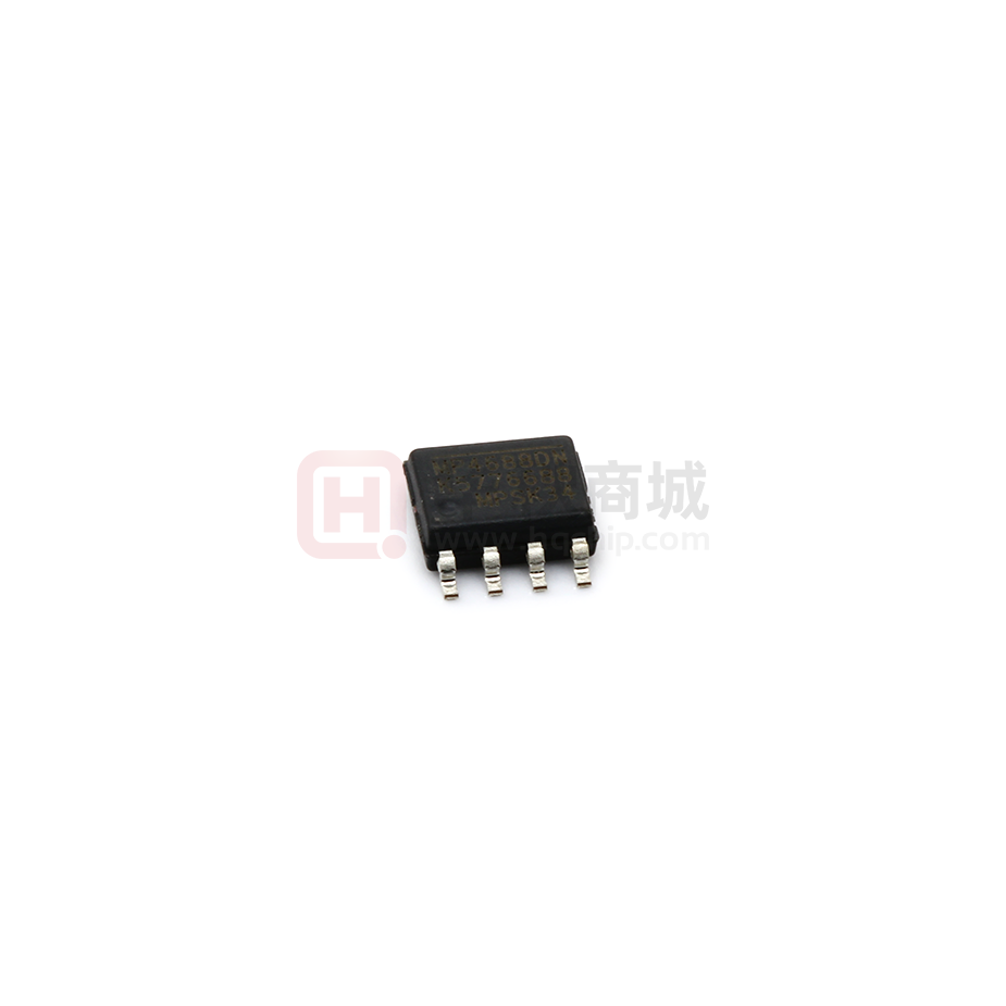
The MP4688 is available in SOIC8 and SOIC8
with exposed pad packages.
•
•
•
•
•
Wide 4.5V to 80V Operating Input Range
No Output Capacitor Required
±5% LED Current Accuracy
Hysteretic Control: No Compensation
Up to 2MHz Switching Frequency
Up to 20kHz Dimming Frequency
Dedicated PWM Dimming Control Input
Short circuit protection with integrated high
side MOSFET
Thermal shut down
200mV reference voltage for high efficiency
Up to 95% Efficiency
170μA Quiescent Current
Available in SOIC8 and SOIC8 with
Exposed Pad Packages
APPLICATIONS
•
•
•
High Power LED Driver
Automotive, Industry and General Lighting
Constant Current Source
All MPS parts are lead-free and adhere to the RoHS directive. For MPS green
status, please visit MPS website under Quality Assurance.
“MPS” and “The Future of Analog IC Technology” are Registered Trademarks of
Monolithic Power Systems, Inc.
TYPICAL APPLICATION
MP4688 Rev. 1.2
7/15/2014
www.MonolithicPower.com
MPS Proprietary Information. Patent Protected. Unauthorized Photocopy and Duplication Prohibited.
© 2014 MPS. All Rights Reserved.
1
�MP4688 – 80V INPUT, 1A HIGH POWER LED DRIVER
ORDERING INFORMATION
Part Number*
Package
Top Marking
Free Air Temperature (TA)
MP4688DN
MP4688DS
SOIC8E
SOIC8
MP4688DN
MP4688DS
–40°C to +85°C
–40°C to +85°C
* For Tape & Reel, add suffix –Z (e.g. MP4688DN–Z);
For RoHS compliant packaging, add suffix –LF (e.g. MP4688DN–LF–Z)
* For Tape & Reel, add suffix –Z (e.g. MP4688DS–Z);
For RoHS compliant packaging, add suffix –LF (e.g. MP4688DS–LF–Z)
PACKAGE REFERENCE
TOP VIEW
SOIC8E
FB
1
8
GND
N/C
2
7
EN
VIN
3
6
DIM
BST
4
5
SW
SOIC8
(4)
ABSOLUTE MAXIMUM RATINGS (1)
Thermal Resistance
Supply Voltage (VIN).................... –0.3V to +80V
Switch Voltage (VSW)............ –0.5V to VIN + 0.5V
BST to SW .................................... –0.3V to +6V
All Other Pins ................................ –0.3V to +6V
Junction Temperature .............................. 150°C
Continuous Power Dissipation (TA = +25°C) (2)
SOIC8E (Exposed Pad) .............................2.5W
SOIC8........................................................1.3W
Lead Temperature ................................... 260°C
Storage Temperature .............. –65°C to +150°C
SOIC8E (Exposed Pad) .......... 50 ...... 10 ... °C/W
SOIC8 ................................... 96 ...... 45 ... °C/W
Recommended Operating Conditions
(3)
Supply Voltage VIN .......................... 4.5V to 75V
EN and DIM Voltages .......................... 0V to 5V
Operating Junct. Temp. .......... –40°C to +125°C
MP4688 Rev. 1.2
7/15/2014
θJA
θJC
Notes:
1) Exceeding these ratings may damage the device.
2) The maximum allowable power dissipation is a function of the
maximum junction temperature TJ(MAX), the junction-toambient thermal resistance θJA, and the ambient temperature
TA. The maximum allowable continuous power dissipation at
any ambient temperature is calculated by PD(MAX)=(TJ(MAX)TA)/θJA. Exceeding the maximum allowable power dissipation
will cause excessive die temperature, and the regulator will go
into thermal shutdown. Internal thermal shutdown circuitry
protects the device from permanent damage.
3) The device is not guaranteed to function outside of its
operating conditions.
4) Measured on JESD51-7 4-layer board.
www.MonolithicPower.com
MPS Proprietary Information. Patent Protected. Unauthorized Photocopy and Duplication Prohibited.
© 2014 MPS. All Rights Reserved.
2
�MP4688 – 80V INPUT, 1A HIGH POWER LED DRIVER
ELECTRICAL CHARACTERISTICS
VIN = 60V, TA= +25°C, unless otherwise noted.
Specifications over temperature are guaranteed by design and characterization.
Parameter
Symbol Condition
VIN UVLO Threshold
VIN UVLO Hysteresis
Shutdown Supply Current
Quiescent Supply Current
(5)
Upper Switch On Resistance
Upper Switch Leakage Current
Current Limit
EN Up Threshold
EN Threshold Hysteresis
EN Input Current
EN Sinking Current
DIM Up Threshold
DIM Threshold Hysteresis
DIM Input Current
RDS(ON)
ISWLK
IPK
VENH
VENHY
IENI
IENS
VDIMH
VDIMHY
IDIM
DIM On Propagation Delay
TDIMDH
DIM Off Propagation Delay
TDIMDL
Feedback Voltage Threshold High
Feedback Voltage Threshold Low
(5)
(5)
Feedback Average Voltage
FB Pin Input Current
VFBH
VFBL
VFB
IFB
FB Propagation Delay to Output
High
TFBDH
FB Propagation Delay to Output
High
TFBDL
Thermal Shutdown
VEN = 0V
No load, VFB = 250mV
VBST – VSW = 5V
VEN = 0V, VSW = 0V
VFB = 0.15V
Min
Typ
Max
Units
3.6
4.0
0.4
2
170
360
0.01
3.2
1.55
320
0.01
2
1.15
300
4.4
V
V
µA
µA
mΩ
µA
A
V
mV
µA
µA
V
mV
µA
2.5
1.4
VEN =5V
VEN =2V
0.8
VDIM =5V or 0V
VFB=0V, VDIM Rising edge to
VSW Rising Edge
VFB=0V, VDIM Falling edge to
VSW Falling Edge
4.5V < VIN < 75V, VFB rising
from 0V until VSW < 30V
4.5V < VIN < 75V, VFB falling
from 0.25V until VSW > 30V
VFB=5V or 0V
Falling edge of VFB from
0.25V to 0V to VSW rising
edge
Rising edge of VFB from 0V
to
0.25V to VSW falling edge
Hysteresis = 20°C
-1
190
-300
5
220
1
1.7
1
3
1.5
1
50
ns
50
ns
215
mV
185
mV
200
210
300
mV
nA
100
ns
100
ns
150
°C
Note:
5) Guaranteed by design.
MP4688 Rev. 1.2
7/15/2014
www.MonolithicPower.com
MPS Proprietary Information. Patent Protected. Unauthorized Photocopy and Duplication Prohibited.
© 2014 MPS. All Rights Reserved.
3
�MP4688 – 80V INPUT, 1A HIGH POWER LED DRIVER
PIN FUNCTIONS
SOIC8E SOIC8
Pin #
Pin #
Name
Description
Feedback. This is the input to hysteretic comparators. An external current sensing
resistor is connected in series with the LEDs to GND. The feedback voltage is
connected to this pin and is regulated at +200mV with 15% current ripple.
Not connected
Input Supply. This supplies power to all the internal control circuitry, both BS
regulators and the high-side switch. A decoupling capacitor to ground must be
placed close to this pin to minimize switching spikes.
Bootstrap. This is the positive power supply for the internal floating high-side
MOSFET driver. Connect a bypass capacitor between this pin and SW pin.
Switch Node. This is the output from the high-side switch. A low VF Schottky
rectifier to ground is required. The rectifier must be close to the SW pins to reduce
switching spikes.
PWM Dimming Input. Pulling this pin below the specified threshold for dimming off.
Pulling it up above the specified threshold for dimming on. If there is no need for
dimming function, connect DIM and EN pins together.
1
1
FB
2
2
N/C
3
3
VIN
4
4
BST
5
5
SW
6
6
DIM
7
7
EN
Enable Input. Pulling this pin below the specified threshold shuts the chip down.
Pulling it up above the specified threshold or leaving it floating enables the chip.
8
8
GND,
Exposed
pad
Ground. It should be connected as close as possible to the output capacitor
avoiding the high current switch paths. Connect exposed pad to GND plane for
optimal thermal performance.
MP4688 Rev. 1.2
7/15/2014
www.MonolithicPower.com
MPS Proprietary Information. Patent Protected. Unauthorized Photocopy and Duplication Prohibited.
© 2014 MPS. All Rights Reserved.
4
�MP4688 – 80V INPUT, 1A HIGH POWER LED DRIVER
BLOCK DIAGRAM
Figure 1—Function Block Diagram
MP4688 Rev. 1.2
7/15/2014
www.MonolithicPower.com
MPS Proprietary Information. Patent Protected. Unauthorized Photocopy and Duplication Prohibited.
© 2014 MPS. All Rights Reserved.
5
�MP4688 – 80V INPUT, 1A HIGH POWER LED DRIVER
TYPICAL PERFORMANCE CHARACTERISTICS
L=47μH, 1 LED Load, TA=25 oC, unless otherwise noted.
MP4688 Rev. 1.2
7/15/2014
www.MonolithicPower.com
MPS Proprietary Information. Patent Protected. Unauthorized Photocopy and Duplication Prohibited.
© 2014 MPS. All Rights Reserved.
6
�MP4688 – 80V INPUT, 1A HIGH POWER LED DRIVER
OPERATION
Hysteresis Current Control with Adaptive
Threshold Adjustment
MP4688 operates in a hysteresis current control
mode to regulate the LED current accurately.
FB pin is the sensed voltage of LED current
across the sensing resistor. The power
MOSFET is turned on and remains on until FB
pin rises to 215mV. The power MOSFET is
turned off and remains off until FB pin falls to
185mV. The two thresholds of 215mV and
185mV are adaptive adjusted to compensate all
the circuit delays so that the LED current is
regulated very accurately with 200mV average
value at FB pin.
Enable Control
The MP4688 has a dedicated enable control pin
(EN) with the positive logic. Its falling threshold
is a precision 1.2V, and its rising threshold is
1.5V (300mV higher).
When floating, EN is pulled up to about 3.0V by
an internal 1µA current source so it is enabled.
To pull it down, over 1µA current capability is
needed.
Thermal Shutdown
Thermal shutdown is implemented to prevent
the chip from operating at exceedingly high
temperatures. When the silicon die temperature
is higher than its upper threshold, it shuts down
the whole chip. When the temperature is lower
than its lower threshold, the chip is enabled
again.
LED Short Protection
The LED current is well regulated with FB pin
voltage at 200mV. As long as the LED sensing
resistor is not failed, the output current is within
limitation. If the LED sensing resistor is failed or
the output is shorted to GND directly, the FB pin
voltage is low even the power MOSFET is
turned on. The power MOSFET will be shut off
if such failure time is longer than 10us. MP4688
will retry the operation after about 300us delay.
The power MOSFET current is also accurately
sensed via a current sense MOSFET. If the
current is over 3.2A, the IC is shut down. This
offers extra protection under output short
conditions.
Floating Driver and Bootstrap Charging
The floating power MOSFET driver is powered
by an external bootstrap capacitor. This floating
driver has its own UVLO protection. This
UVLO’s rising threshold is 2.2V with a threshold
of 150mV.
The bootstrap capacitor is charged and
regulated to about 5V by the dedicated internal
bootstrap regulator.
In case the internal circuit does not have
sufficient voltage and the bootstrap capacitor is
not well charged, extra external circuitry can be
used to ensure the bootstrap voltage is in the
normal operational region. Refer to External
Bootstrap Diode in Application section.
Under-Voltage Lockout (UVLO)
Under-voltage lockout (UVLO) is implemented
to protect the chip from operating at insufficient
supply voltage. The UVLO rising threshold is
about 4.0V while its falling threshold is a
consistent 3.65V.
MP4688 Rev. 1.2
7/15/2014
www.MonolithicPower.com
MPS Proprietary Information. Patent Protected. Unauthorized Photocopy and Duplication Prohibited.
© 2014 MPS. All Rights Reserved.
7
�MP4688 – 80V INPUT, 1A HIGH POWER LED DRIVER
APPLICATION INFORMATION
COMPONENT SELECTION
Setting the LED Current
The LED current ILED is set using a sensing
resistor RFB, which is in series with the LEDs
and connected to GND. The voltage on the
sensing resistor RFB is connected to FB pin.
ILED =
VFB
RFB
For example, for a 700mA LED current, RFB is
287mΩ.
The input current to the step-down converter is
discontinuous, therefore a capacitor is required
to supply the AC current to the step-down
converter while maintaining the DC input
voltage. Use low ESR capacitors for the best
performance especially under high switching
frequency applications.
The RMS current through the input capacitor is
about:
ID = ILED ⋅
Inductor Selection and Frequency Setting
The inductor LO is required to supply a constant
current to the LED. The inductor value is related
to the switching frequency fs setting:
fs =
(
VOUT ⋅ ( VIN − VOUT )
VIN ⋅ 8 ⋅ 10−8 ⋅ VIN + L ⋅ 15% ⋅ ILED
)
Where, VIN is the input voltage, VOUT is the
output voltage to drive the LEDs. A larger value
inductor will result in smaller switching
frequency.
The peak inductor current is about:
⎛ 4 ⋅ 10 −8 ⋅ VIN
⎞
+ 1.075 ⎟
ILP = ILED ⋅ ⎜
⎝ L ⋅ ILED
⎠
Choose an inductor that will not saturate under
the maximum inductor peak current.
Output Rectifier Diode
The output rectifier diode supplies the current to
the inductor when the high-side switch is off. To
reduce losses due to the diode forward voltage
and recovery times, use a Schottky diode.
With low ESR capacitors, the input voltage
ripple can be estimated by:
ΔVIN =
VOUT
VIN
⎛ V ⎞
V
ILED
× OUT × ⎜ 1 − OUT ⎟
fs × CIN VIN ⎝
VIN ⎠
Choose the input capacitor with enough RMS
current rating and enough capacitance for small
input voltage ripple.
When electrolytic or tantalum capacitors are
applied, a small, high quality ceramic capacitor,
i.e. 0.1μF, should be placed as close to the IC
as possible.
Output Capacitor COUT
The output capacitor (COUT) is not necessary for
MP4688. The LED current ripple (peak-to-peak
value) is about 15% of the LED DC current.
Output capacitor can be used to further reduce
the LED current ripple. Low ESR capacitors are
preferred to keep the output voltage ripple low
so that the AC ripple current through the LEDs
is small. The output voltage ripple can be
estimated by:
The RMS current through the diode is about:
ID = ILED ⋅ 1 −
VOUT
’
VIN
ΔVOUT =
VOUT ⎛
V
× ⎜ 1 − OUT
fS × L O ⎝
VIN
⎞
⎞ ⎛
1
⎟
⎟ × ⎜ RESR +
8 × fS × COUT ⎠
⎠ ⎝
Choose a diode whose maximum reverse
voltage rating is greater than the maximum
input voltage, and whose current rating is
greater than the maximum diode current.
Input Capacitor CIN
MP4688 Rev. 1.2
7/15/2014
www.MonolithicPower.com
MPS Proprietary Information. Patent Protected. Unauthorized Photocopy and Duplication Prohibited.
© 2014 MPS. All Rights Reserved.
8
�MP4688 – 80V INPUT, 1A HIGH POWER LED DRIVER
Where RESR is the equivalent series resistance
(ESR) value of the output capacitor.
Try to run the feedback trace as far from the
inductor and noisy power traces as possible. It
is often a good idea to run the feedback trace
on the side of the PCB opposite of the inductor
with a ground plane separating the two.
External Bootstrap Diode
An external bootstrap diode may enhance the
efficiency of the LED driver. In below cases, an
external BST diode is recommended from the
5V to BST pin:
z
There is a 5V rail available in the system;
z
VIN is no greater than 5V;
z
VOUT is between 3.3V and 5V;
To help to improve the thermal conduction, a
grid of thermal vias can be created right under
the exposed pad. It is recommended that they
be small (15mil barrel diameter) so that the hole
is essentially filled up during the plating process,
thus aiding conduction to the other side. Too
large a hole can cause ‘solder wicking’
problems during the reflow soldering process.
The pitch (distance between the centers) of
several such thermal vias in an area is typically
40mil.
This diode is also recommended for high duty
cycle operation (when VOUT/VIN>65%) and very
high frequency (over 1.5MHz) applications.
The bootstrap diode can be a low cost one
such as IN4148 or BAT54.
Reference design
Street lighting and flat panel lighting are
transiting to more efficient sources of light. LED
light source will become the trend in the near
future. This reference design provides a flexible
solution for street lighting and flat panel lighting
application by utilizing MP4688 featuring high
reliability, high efficiency, and accurate current
regulation.
5V
BS
MP4560
MP4688
SW
Figure 2—External Bootstrap Diode
Specifications
Layout Consideration
Parameter
Input Voltage
Enable/Dimming
LED Current
It is essential to place the input decoupling
capacitor, catch diode and the MP4688 (VIN pin,
SW pin and PGND) as close as possible, with
traces that are very short and fairly wide. This
can help to greatly reduce the voltage spike on
SW node, and lower the EMI noise level as well.
Over
Protection
Current
Symbol
VIN
EN/DIM
ILED
Value
4.5 to 75
5
730
Units
V
V
mA
OCP
3.2
A
Reference schematic
MP4688
VIN
/100V
C1
GND
C2
/100V
C3
1
2
3
4
FB
N/C
VIN
BST
GND
EN
DIM
SW
R4
0
8
7
6
5
EN
R3
DIM
NS
LED+
D1
C5
NC
C7
NC
R1
LED_
R2
MP4688 Rev. 1.2
7/15/2014
www.MonolithicPower.com
MPS Proprietary Information. Patent Protected. Unauthorized Photocopy and Duplication Prohibited.
© 2014 MPS. All Rights Reserved.
9
�MP4688 – 80V INPUT, 1A HIGH POWER LED DRIVER
PACKAGE INFORMATION
SOIC8E (EXPOSED PAD)
0.189(4.80)
0.197(5.00)
0.124(3.15)
0.136(3.45)
8
5
0.150(3.80)
0.157(4.00)
PIN 1 ID
1
0.228(5.80)
0.244(6.20)
0.089(2.26)
0.101(2.56)
4
TOP VIEW
BOTTOM VIEW
SEE DETAIL "A"
0.051(1.30)
0.067(1.70)
SEATING PLANE
0.000(0.00)
0.006(0.15)
0.013(0.33)
0.020(0.51)
0.0075(0.19)
0.0098(0.25)
SIDE VIEW
0.050(1.27)
BSC
FRONT VIEW
0.010(0.25)
x 45o
0.020(0.50)
GAUGE PLANE
0.010(0.25) BSC
0.050(1.27)
0.024(0.61)
0o-8o
0.016(0.41)
0.050(1.27)
0.063(1.60)
DETAIL "A"
0.103(2.62)
0.138(3.51)
RECOMMENDED LAND PATTERN
MP4688 Rev. 1.2
7/15/2014
0.213(5.40)
NOTE:
1) CONTROL DIMENSION IS IN INCHES. DIMENSION IN
BRACKET IS IN MILLIMETERS.
2) PACKAGE LENGTH DOES NOT INCLUDE MOLD FLASH,
PROTRUSIONS OR GATE BURRS.
3) PACKAGE WIDTH DOES NOT INCLUDE INTERLEAD FLASH
OR PROTRUSIONS.
4) LEAD COPLANARITY (BOTTOM OF LEADS AFTER FORMING)
SHALL BE 0.004" INCHES MAX.
5) DRAWING CONFORMS TO JEDEC MS-012, VARIATION BA.
6) DRAWING IS NOT TO SCALE.
www.MonolithicPower.com
MPS Proprietary Information. Patent Protected. Unauthorized Photocopy and Duplication Prohibited.
© 2014 MPS. All Rights Reserved.
10
�MP4688 – 80V INPUT, 1A HIGH POWER LED DRIVER
SOIC8
0.189(4.80)
0.197(5.00)
8
0.050(1.27)
0.024(0.61)
5
0.063(1.60)
0.150(3.80)
0.157(4.00)
PIN 1 ID
1
0.228(5.80)
0.244(6.20)
0.213(5.40)
4
TOP VIEW
RECOMMENDED LAND PATTERN
0.053(1.35)
0.069(1.75)
SEATING PLANE
0.004(0.10)
0.010(0.25)
0.013(0.33)
0.020(0.51)
0.0075(0.19)
0.0098(0.25)
SEE DETAIL "A"
0.050(1.27)
BSC
SIDE VIEW
FRONT VIEW
0.010(0.25)
x 45o
0.020(0.50)
GAUGE PLANE
0.010(0.25) BSC
0o-8o
0.016(0.41)
0.050(1.27)
DETAIL "A"
NOTE:
1) CONTROL DIMENSION IS IN INCHES. DIMENSION IN
BRACKET IS IN MILLIMETERS.
2) PACKAGE LENGTH DOES NOT INCLUDE MOLD FLASH,
PROTRUSIONS OR GATE BURRS.
3) PACKAGE WIDTH DOES NOT INCLUDE INTERLEAD FLASH
OR PROTRUSIONS.
4) LEAD COPLANARITY (BOTTOM OF LEADS AFTER FORMING)
SHALL BE 0.004" INCHES MAX.
5) DRAWING CONFORMS TO JEDEC MS-012, VARIATION AA.
6) DRAWING IS NOT TO SCALE.
NOTICE: The information in this document is subject to change without notice. Users should warrant and guarantee that third
party Intellectual Property rights are not infringed upon when integrating MPS products into any application. MPS will not
assume any legal responsibility for any said applications.
MP4688 Rev. 1.2
7/15/2014
www.MonolithicPower.com
MPS Proprietary Information. Patent Protected. Unauthorized Photocopy and Duplication Prohibited.
© 2014 MPS. All Rights Reserved.
11
�