MP5000S
EC
R NE O
EF W M
ER D M
E
TO ES ND
I
E
G
M
D
N
P5 S F
O
01
R
4A
12V, 5A Programmable Current
Limit Switch
DESCRIPTION
FEATURES
The MP5000S is a protection device designed to
protect circuitry on the output (source) from
transients on input (VCC). It also protects VCC from
undesired shorts and transients coming from the
source.
At start up, inrush current is limited by limiting the
slew rate at the source. The slew rate is
controlled by a small capacitor at the dv/dt pin.
The dv/dt pin has an internal circuit that allows
the customer to float this pin (no connect) and
still receive 0.9ms ramp time at the source.
The maximum load at the output (source) is
current limited. This is accomplished by utilizing a
sense FET topology. The magnitude of the
current limit is controlled by an external resistor
from the I-Limit pin to the Source pin.
Integrated 40mΩ Power FET
Enable/Fault Pin
Adjustable Slew Rate for Output Voltage
Adjustable Current Limit: 1-5A
Thermal Protection
Over Voltage Limit
APPLICATIONS
Hot Swap
PC Cards
Laptops
All MPS parts are lead-free and adhere to the RoHS directive. For MPS green
status, please visit MPS website under Products, Quality Assurance page.
“MPS” and “The Future of Analog IC Technology” are registered trademarks of
Monolithic Power Systems, Inc.
An internal charge pump drives the gate of the
power device, allowing a very low on-resistance
DMOS power FET of just 40mΩ.
R
The source is protected from the VCC input being
too low or too high. Under Voltage Lockout
(UVLO) assures that VCC is above the minimum
operating threshold, before the power device is
turned on. If VCC goes above the high output
threshold, the source voltage will be limited.
N
O
T
TYPICAL APPLICATION
MP5000S Rev. 1.0
www.MonolithicPower.com
4/29/2013
MPS Proprietary Information. Patent Protected. Unauthorized Photocopy and Duplication Prohibited.
© 2013 MPS. All Rights Reserved.
1
�MP5000S – 12V, 1A-5A PROGRAMMABLE CURRENT LIMIT SWITCH
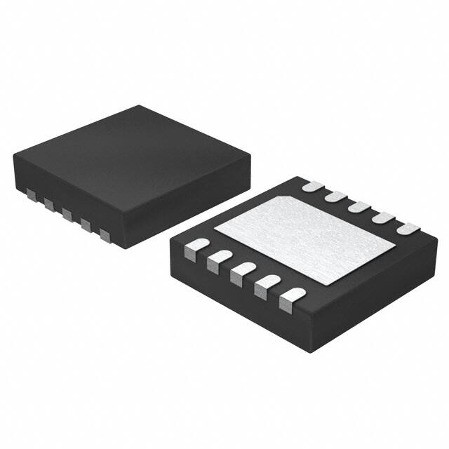
ORDERING INFORMATION
Package
Top Marking
MP5000SDQ
QFN10 (3 x3mm)
ADT
EC
R NE O
EF W M
ER D M
E
TO ES ND
I
E
G
M
D
N
P5 S F
O
01
R
4A
Part Number*
* For Tape & Reel, add suffix –Z (e.g. MP5000SDQ–Z);
For RoHS Compliant Packaging, add suffix –LF (e.g. MP5000SDQ–LF–Z)
PACKAGE REFERENCE
Operating Junction Temp. (TJ). -40°C to +125°C
ABSOLUTE MAXIMUM RATINGS
(1)
R
VCC, SOURCE, I-LIMIT .................. -0.3V to 22V
dv/dt, ENABLE/FAULT..................... -0.3V to 6V
Storage Temperature ............... -65C to +155C
(2)
Continuous Power Dissipation (TA = +25°C)
............................................................2.5W
Operating Junction Temperature . -40C to 150C
Input Voltage Transient (100mS) ......... VIN=25V
Recommended Operating Conditions
T
Input Voltage Operating Range…….10V to 18V
Continuous Current
0.5 in2 pad .................................................4.2A
For Minimum Copper, TA=80°C...................2.3A
O
N
(3)
Thermal Resistance
(4)
θJA
θJC
QFN10 .................................... 50 ...... 12 ... C/W
Notes:
1) Exceeding these ratings may damage the device.
2) The maximum allowable power dissipation is a function of the
maximum junction temperature TJ(MAX), the junction-toambient thermal resistance θJA, and the ambient temperature
TA. The maximum allowable continuous power dissipation at
any ambient temperature is calculated by PD(MAX)=(TJ(MAX)TA)/ θJA. Exceeding the maximum allowable power dissipation
will cause excessive die temperature, and the regulator will go
into thermal shutdown. Internal thermal shutdown circuitry
protects the device from permanent damage.
3) The device is not guaranteed to function outside of its
operating conditions.
4) Measured on JESD51-7, 4-layer PCB.
MP5000S Rev. 1.0
www.MonolithicPower.com
4/29/2013
MPS Proprietary Information. Patent Protected. Unauthorized Photocopy and Duplication Prohibited.
© 2013 MPS. All Rights Reserved.
2
�MP5000S – 12V, 1A-5A PROGRAMMABLE CURRENT LIMIT SWITCH
ELECTRICAL CHARACTERISTICS
VCC = 12V, RLIMIT=22Ω, Capacitive Load = 100μF, TA=25°C, unless otherwise noted.
Symbol
Delay Time
tDLY
ON Resistance
(5)
RDSon
Off State Output Voltage
VOFF
Thermal Latch
(5)
Shutdown Temperature
Under/Over Voltage Protection
TSD
Output Clamping Voltage
VCLAMP
Under Voltage Lockout
VUVLO
Under Voltage Lockout (UVLO)
Hysteresis
Current Limit
(6)
Hold Current
Trip Current
dv/dt Circuit
ILIM-SS
ILIM-OL
Rise Time
Tr
Enable/Fault
Low Level Input Voltage
VIL
VI (INT)
High Level Input Voltage
High State Maximum Voltage
Low Level Input Current (Sink)
VIH
VI (MAX)
IIL
R
Intermediate Level Input Voltage
T
Maximum Voltage on Enable/Fault
(7)
Pin
Total Device
O
Min
Enabling
of
chip
to
ID=100mA with a 1A resistive
load
TJ=25°C
TJ=85°C
VCC=18Vdc, VENABLE=0Vdc,
RL= 500Ω
Typ
Max
Units
0.1
40
52
IBIAS
Minimum Operating Voltage for
UVLO
VMIN
55
mΩ
mV
175
Overvoltage Protection
VCC=17V
Turn on,
Voltage going high
°C
13.8
15
16.2
V
7.7
8.5
9.3
V
0.80
RLIM=22Ω
RLIM=22Ω
Float dv/dt pin, Enable to
VOUT=12V
Output Disabled
Thermal
Fault,
Disabled
Output Enabled
Output
VENABLE=0V
Total number of chips that
can be connected for
simultaneous shutdown
V
2.4
3.7
5.0
5.0
A
A
0.5
0.9
2.1
ms
0.5
V
1.95
V
-50
V
V
μA
3
Units
VCC
V
0.82
1.4
2.5
5
-28
VMAX
Bias Current
ms
120
VHYST
Maximum Fanout for Fault Signal
N
Condition
EC
R NE O
EF W M
ER D M
E
TO ES ND
I
E
G
M
D
N
P5 S F
O
01
R
4A
Parameters
Power FET
Device Operational
1
Thermal Shutdown
0.4
Enable
很抱歉,暂时无法提供与“MP5000SDQ-LF-Z”相匹配的价格&库存,您可以联系我们找货
免费人工找货- 国内价格
- 1+11.03780
- 10+8.16500
- 100+6.99860
- 1000+5.83210
- 国内价格 香港价格
- 1+11.012521+1.42271