MP5006
5V, 1A- 5A Programmable Current
Limit Switch with Slew Rate Control and
Auto Enable
The Future of Analog IC Technology
DESCRIPTION
FEATURES
The MP5006 is a protection device designed to
protect circuitry on the output (VOUT) from
transients on input (VIN). It also protects VIN from
undesired shorts and transients coming from the
load.
•
•
•
•
•
At start up, inrush current is controlled by limiting
the slew rate at the VOUT. The slew rate is
controlled by a small capacitor at the dv/dt pin.
The dv/dt pin has an internal circuit that allows
the customer to float this pin (no connect) and
still receive a 1.1ms ramp time at the VOUT.
The max load at the output (VOUT) is current
limited. This is accomplished by utilizing a sense
FET topology. The magnitude of the current limit
is controlled by an external resistor connected
between the ILIMIT pins.
Integrated 44mΩ Power FET
Enable/Fault Pin
Adjustable Slew Rate for Output Voltage
Adjustable Current Limit
Automatic Startup/Retry after Thermal
Protection
Over Voltage Limit
•
APPLICATIONS
•
•
•
•
•
Hot Swap
PC Cards
Laptops
SSD
HDD
“MPS” and “The Future of Analog IC Technology” are Registered Trademarks
of Monolithic Power Systems, Inc.
An internal charge pump drives the gate of the
power device, allowing a very low on-resistance
DMOS power FET of just 0.044Ω.
VOUT is protected from VIN being too low or too
high. Under Voltage Lockout (UVLO) assures
that the input is above the minimum operating
threshold, before the power device is turned on.
If VIN goes above the high output threshold, the
output voltage will be limited.
TYPICAL APPLICATION
VIN
11
6
+ILIMIT
VIN
RLimit
7 -ILIMIT
8
EN
Cdv/dt
(Optinal)
MP5006 Rev.0.92
12/27/2013
VOUT
MP5006
Enable/Fault
9 dv/dt
10
VOUT
GND
VOUT
VOUT
5
VOUT
4
3
2
VOUT 1
www.MonolithicPower.com
MPS Proprietary Information. Unauthorized Photocopy and Duplication Prohibited.
© 2013 MPS. All Rights Reserved.
1
�MP5006 – 5V, 1A- 5A PROGRAMMABLE CURRENT LIMIT SWITCH WITH AUTO ENABLE
ORDERING INFORMATION
Part Number*
MP5006EQ
Package
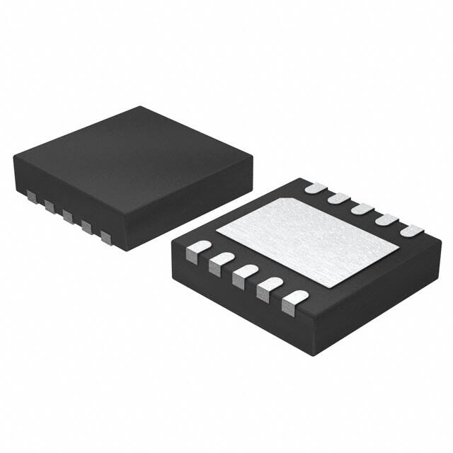
QFN10 (3x3)
Top Marking
8M
Free Air Temperature (TA)
–20°C to +85°C
* For Tape & Reel, add suffix –Z (e.g. MP5006EQ–Z).
For RoHS Compliant Packaging, add suffix –LF (e.g. MP5006EQ–LF–Z)
PACKAGE REFERENCE
TOP VIEW
VOUT
1
VOUT
2
VOUT
3
VOUT
4
VOUT
5
10 GND
EXPOSED
PAD
VIN
ABSOLUTE MAXIMUM RATINGS (1)
VIN, VOUT, +ILIMIT, -ILIMIT .................................. 22V
dv/dt, ENABLE/FAULT .................................. 6V
Junction Temperature..................... –20°C to +150°C
(2)
Continuous Power Dissipation (TA=+25oC)
…………………………………………………2.5W
Storage Temperature.............. –65°C to +155°C
Recommended Operating Conditions
Input Voltage Operating Range ......... 4V to 10V
Operating Junct. Temp (TJ)....... –20°C to +125°C
MP5006 Rev.0.92
12/27/2013
9
dv/dt
8
ENABLE/FAULT
7
-ILIMIT
6
+ILIMIT
Thermal Resistance
(3)
……..θJA θJC
QFN10 ....................................50 ...... 12 ... °C/W
Notes:
1) Exceeding these ratings may damage the device.
2) The maximum allowable power dissipation is a function of the
maximum junction temperature TJ(MAX) , the junction-toambient thermal resistance θJA,and the ambient temperature
TA, the maximum allowable power dissipation at any ambient
temperature is calculated using: PD(MAX)=(TJ(MAX)-TA)/ θJA.
Exceeding the maximum allowable power dissipation will
cause excessive die temperature, and the regulator will go
into thermal shutdown. Internal thermal shutdown circuitry
protects the device from permanent damage.
o
Reduce 0.2 Watts for every 10 C ambient temperature
increasing
3) Measured on JESD51-7 4-layer board.
www.MonolithicPower.com
MPS Proprietary Information. Unauthorized Photocopy and Duplication Prohibited.
© 2013 MPS. All Rights Reserved.
2
�MP5006 – 5V, 1A- 5A PROGRAMMABLE CURRENT LIMIT SWITCH WITH AUTO ENABLE
ELECTRICAL CHARACTERISTICS
VIN =5V, RLIMIT=24Ω, COUT=10μF, TJ=25°C, unless otherwise noted.
Parameters
Power FET
Symbol
Delay Time
tDLY
ON Resistance
RDSon
Off State Output Voltage
VOFF
Continuous Current
ID
Thermal Shutdown
Shutdown Temperature
Under/Over Voltage Protection
TSD
Output Clamping Voltage
VCLAMP
Under Voltage Lockout
VUVLO
Under Voltage Lockout (UVLO)
Hysteresis
Current Limit
Hold Current
Trip Current
dv/dt Circuit
Rise Time
Enable/Fault
Low Level Input Voltage
High Level Input Voltage
High State Maximum Voltage
Low Level Input Current (Sink)
Condition
Enabling
of
chip
to
ID=100mA with a 12Ω
resistive load
TJ=25°C
TJ=80°C, Note 4
VIN =18Vdc, Enable=0V,
RL=500Ω
0.5 in2 pad, Note 4,
TJ=25°C
ILIM-SS
ILIM-OL
ms
82
mΩ
mV
A
175
°C
5
5.4
5.9
V
3.2
3.6
4.0
V
0.2
V
RLIMIT=24Ω, Note 4
RLIMIT=24Ω, Note 4
1.2
2.3
1.55
3
1.9
3.7
A
A
Tr
Float dv/dt pin, Note 5
0.64
1.1
2.0
ms
VIL
VIH
Output Disabled
Output Enabled
0.5
2.5
V
V
V
-80
μA
5
Units
VIN
V
VI (MAX)
IIL
VENABLE=0V
Total number of chips that
can be connected for
simultaneous shutdown
Note 6
Bias Current
IBIAS
Device Operational
Thermal Shutdown
VMIN
Enable 6V. Maximum Input Voltage to be VIN if VIN ≤ 6V.
MP5006 Rev.0.92
12/27/2013
www.MonolithicPower.com
MPS Proprietary Information. Unauthorized Photocopy and Duplication Prohibited.
© 2013 MPS. All Rights Reserved.
3
�MP5006 – 5V, 1A- 5A PROGRAMMABLE CURRENT LIMIT SWITCH WITH AUTO ENABLE
PIN FUNCTIONS
Pin #
1-5
6
7
8
9
10
11
Description
This pin is the VOUT of the internal power FET and the output terminal of the IC.
A resistor between these pins sets the overload and short circuit current limit levels.
A resistor between these pins sets the overload and short circuit current limit levels.
The Enable/Fault pin is a bi-directional interface. It can be used to enable the output
of the device by floating the pin, or disable the chip by pulling it to ground (using an
Enable/Fault
open drain or open collector device). If a thermal fault occurs, the voltage on this pin
will drive to ground, automatically.
The internal dv/dt circuit controls the slew rate of the output voltage at turn on. It has
an internal capacitor that allows it to ramp up over the period of 1.1ms. An external
dv/dt
capacitor can be added to this pin to increase the ramp time. If an additional time
delay is not required, this pin should be left open.
GND
Negative Input Voltage to the Device. This is used as the internal reference for the IC.
VIN
Positive input voltage to the device (Exposed Pad).
MP5006 Rev.0.92
12/27/2013
Name
VOUT
+ILIMIT
-ILIMIT
www.MonolithicPower.com
MPS Proprietary Information. Unauthorized Photocopy and Duplication Prohibited.
© 2013 MPS. All Rights Reserved.
4
�MP5006 – 5V, 1A- 5A PROGRAMMABLE CURRENT LIMIT SWITCH WITH AUTO ENABLE
TYPICAL PERFORMANCE CHARACTERISTICS
VIN =5V, VEN =3.3V, RLIMIT=24Ω, COUT =10μF, Cdv/dt =1nF, TA =25°C, unless otherwise noted.
Supply Current,Output Enabled Supply Current,Output Disabled Static Drain-Source On-State
vs.Input Voltage
Resistance vs. Input Voltage
vs.Input Voltage
VEN=0V
No load, EN floating
1. 8
1. 75
1. 7
1. 65
4
4.5
5
59
57
55
0.96
53
0.94
51
49
0.92
47
0.9
3.5
5.5
4
4.5
5
45
5.5
140
VIN=4V
VIN=4.5V
VIN=5V
80
60
VIN=5.5V
40
20
0
0 .5
1
1 .5
2
2 .5
3
H O LD C U R R EN T(A )
100
2 .9
2 .8
2 .7
2.6
3 .5
LOAD CURRENT(A)
4
4 .5
5
12
8
4
3
6
9
1.6
1.5
1.4
3 .5
5 .5
12 15 18 21 24
4
4 .5
5
5 .5
INPUT VOLTAGE(V)
Trip and Hold Current
vs. RLIMIT
TRIP CURRENT & HOLD CURRENT(A)
RESPONSE TIME(us)
No Cout
5.5
1.7
INPUT VOLTAGE(V)
Current Limit Response
vs. Peak Current
16
4
4.5
5
INPUT VOLTAGE (V)
1.8
3 .1
120
3.5
INP UT V OL T AG E (V )
TRIP CURRENT(A)
INPUT TO OUTPUT VOLTAGE(mV)
61
0.98
INP UT VO L T AG E (V)
0
IOUT=1A
1
S UP P L Y C UR R E NT (mA)
S UP P L Y C UR R E NT (mA )
1. 85
6
5
4
Trip Current
3
2
1
Hold Current
0
0
20
40
60
80
100 120
PEAK CURRENT(A)
MP5006 Rev.0.92
12/27/2013
www.MonolithicPower.com
MPS Proprietary Information. Unauthorized Photocopy and Duplication Prohibited.
© 2013 MPS. All Rights Reserved.
5
�MP5006 – 5V, 1A- 5A PROGRAMMABLE CURRENT LIMIT SWITCH WITH AUTO ENABLE
TYPICAL PERFORMANCE CHARACTERISTICS (continued)
VIN =5V, VEN =3.3V, RLIMIT=24Ω, COUT =10μF, Cdv/dt =1nF, TA =25°C, unless otherwise noted.
Turn on Delay and Rise Time
Turn on Delay and Rise Time
Turn off Delay and Fall Time
Cdv/dt=1nF,COUT=10uF,no load
No Cdv/dt,COUT=10uF,no load
No Cdv/dt,COUT=10uF,no load
VOUT
2V/div
EN
2V/div
VOUT
2V/div
VOUT
2V/div
EN
2V/div
EN
2V/div
400ms/div
400us/div
10ms/div
Short Circuit Current,
Device Enabled into Short
No Cdv/dt
VOUT
2V/div
VOUT
2V/div
EN
2V/div
EN
2V/div
IOUT
1A/div
IOUT
1A/div
EN
2V/div
IOUT
1A/div
400us/div
100us/div
Short Circuit Current,
Device Enabled into Short,
and Thermal Shut down
and Auto Start Up
100us/div
Trip Current with Ramped
Load on Enabled Device
Inrush Current with Different
Load Capacitance
No Cdv/dt
No Cdv/dt
EN Floating, No Cdv/dt
VOUT
2V/div
EN
2V/div
2200uF
EN
2V/div
1000uF
470uF
100ms/div
MP5006 Rev.0.92
12/27/2013
IOUT
500mA/div
IOUT
1A/div
IOUT
1A/div
4ms/div
www.MonolithicPower.com
MPS Proprietary Information. Unauthorized Photocopy and Duplication Prohibited.
© 2013 MPS. All Rights Reserved.
1ms/div
6
�MP5006 – 5V, 1A- 5A PROGRAMMABLE CURRENT LIMIT SWITCH WITH AUTO ENABLE
TYPICAL PERFORMANCE CHARACTERISTICS (continued)
VIN =5V, VEN =3.3V, RLIMIT=24Ω, COUT =10μF, Cdv/dt =1nF, TA =25°C, unless otherwise noted.
Current Limit
(trip hold thermal shut down)
Auto Start Up)
No Cdv/dt
VOUT
2V/div
Peak Current
VOUT
2V/div
VOUT
2V/div
Peak Current
IOUT
2A/div
Response Time
20us/div
MP5006 Rev.0.92
12/27/2013
IOUT
2A/div
Response Time
20us/div
IOUT
1A/div
100ms/div
www.MonolithicPower.com
MPS Proprietary Information. Unauthorized Photocopy and Duplication Prohibited.
© 2013 MPS. All Rights Reserved.
7
�MP5006 – 5V, 1A- 5A PROGRAMMABLE CURRENT LIMIT SWITCH WITH AUTO ENABLE
BLOCK DIAGRAM
VIN
Enable/
Fault
Enable
Charge
Pump
VOUT
Thermal
Shutdown
Current
Limit
-ILIMIT
+ILIMIT
UVLO
Voltage
Clamp
dv/dt
Control
dv/dt
GND
Figure 1—Function Block Diagram
MP5006 Rev.0.92
12/27/2013
www.MonolithicPower.com
MPS Proprietary Information. Unauthorized Photocopy and Duplication Prohibited.
© 2013 MPS. All Rights Reserved.
8
�MP5006 – 5V, 1A- 5A PROGRAMMABLE CURRENT LIMIT SWITCH WITH AUTO ENABLE
CURRENT LIMIT
The desired current limit is a function of the
external current limit resistor.
RISE TIME
The rise time is a function of the capacitor (Cdv/dt)
on the dv/dt pin.
Table 1―Current Limit vs. Current Limit Resistor
(VIN =5V)
Table 2―Rise Time vs. Cdv/dt
Current Limit Resistor
(Ω)
Trip Current
(A)
Hold Current
(A)
24
50
75
100
3
2
1.78
1.67
1.55
0.76
0.5
0.38
When the part is active, if load reaches trip
current (minimum threshold current triggering
overcurrent protection) or a short is present, the
part switches into to a constant-current (hold
current) mode. Part will enter thermal cycling only
if the overcurrent condition stays long enough to
trigger thermal protection.
However, when the part is powered up by VCC or
EN, the load current should be smaller than hold
current. Otherwise, the part can’t be fully turned
on.
In a typical application using a current limit
resistor of 24Ω, the trip current will be 3A and the
hold current will be 1.55A. If the device is in its
normal operating state and passing 1.55A it will
need to dissipate only 105.7mW with the very low
on resistance of 44mΩ. For the package
dissipation of 50°C/Watt, the temperature rise will
only be + 5.3°C. Combined with a 25°C ambient,
this is only 30.3°C total package temperature.
During a short circuit condition, the device now
has 5V across it and the hold current clamps at
1.55A and therefore must dissipate 7.75W. At
50°C/watt, if uncontrolled, the temperature would
rise above the MP5006 thermal protection
(+175°C) and shutdown the device to cause the
temperature to drop below a hysteresis level.
Proper heat sink must be used if the device is
intended to supply the hold current and not
shutdown. Without a heat sink, hold current
should be maintained below 600mA at + 25°C
and below 360mA at +85°C to prevent the device
from activating the thermal shutdown.
MP5006 Rev.0.92
12/27/2013
Cdv/dt
Rise Time*
(TYPICAL)
(ms)
none
50pF
500pF
1nF
1.1
2.2
12.3
23.5
* Notes: Rise Time = KRT*(50pF+Cdv/dt), KRT =22E6
The “rise time” is measured by from 10% to 90%
of output voltage.
U
Input
Output
90%
Enable
10%
Rise Time
t
Figure 2―Rise Time
FAULT AND ENABLE PIN
The Enable/Fault Pin is a Bi-Directional I/O with a
weak pull up current (25uA typical). It functions to
enable/disable the part.
Enable pin as an input:
1. Low disables the part.
2. High enables the part.
Enable pin as an output:
1. The pull up current may (if not over
ridden) allow a “wired nor” pull up to
enable the part.
2. An under voltage will cause a low on the
enable pin.
3. A thermal fault will cause a low level on
the enable pin.
www.MonolithicPower.com
MPS Proprietary Information. Unauthorized Photocopy and Duplication Prohibited.
© 2013 MPS. All Rights Reserved.
9
�MP5006 – 5V, 1A- 5A PROGRAMMABLE CURRENT LIMIT SWITCH WITH AUTO ENABLE
There are 4 types of faults, and each fault has a
direct and indirect effect on the Enable/Fault pin
and the internal fault flag. In a typical application
there are one or more of the MP5006 chips in a
system. The Enable/Fault lines will typically be
connected together.
Table 3―Fault Function Influence in Application
Fault description
Short/over current
Internal action
Limit current
Under Voltage
Output is
turned off
Over Voltage
Limit output
voltage
None
None
None
Shutdown part.
The part retries
to start up
automatically
Internally drives
Enable/Fault pin
to low level, and
after part cools
down, Enable/Fault
pin will be pulled
high
Flag is set at
thermal shut
down, and is set
to high after
auto start up.
Secondary part output is
disabled when thermal shut
down, and is enabled after
MP5006 auto start up.
Thermal Shutdown
MP5006 Rev.0.92
12/27/2013
Effect on Fault Pin
none
Internally drives
Enable/Fault pin to
Logic low
Effect on Flag
None
Flag is reset
Effect on secondary Part
none
Secondary part output is
disabled, and fault flag is
reset.
www.MonolithicPower.com
MPS Proprietary Information. Unauthorized Photocopy and Duplication Prohibited.
© 2013 MPS. All Rights Reserved.
10
�MP5006 – 5V, 1A- 5A PROGRAMMABLE CURRENT LIMIT SWITCH WITH AUTO ENABLE
THERMAL PROTECTION
The MP5006 only considers a thermal overload
to be a fault. Under a fault condition the mp5006
will have two actions:
1) Turn off the output power device.
2) Drive the enable/fault pin to the low level.
The power device will remain off until the die
temperature drops below the hysteresis level.
When the die cools down below the thermal
hysteresis level, the MP5006 will restart in the
start up mode and the fault line will be pulled high
through a 25uA pull up current. If the cause of
the fault has been removed, the output will ramp
up in a controlled fashion with the ramp rate
controlled by the dv/dt function. If the cause of
the fault is still present, the excess power
dissipation will heat up the part. When the die
temperature reaches the thermal shutdown
temperature, the output will be turned off and the
enable/fault pin will be driven to the low level,
again. This cycle will repeat until the cause of the
fault is removed.
Figure 3―Thermal Protection in Short Condition
The drawing above shows the initial start up
sequence and the occurrence of a short at the
output.
At time T0 the input voltage begins to rise. At T1
the input voltage rises above the UVLO threshold
and the part starts up. The output current ramps
up and settles at the normal operating current
level until time T2. There is a very small
temperature heating of the die in normal
operation.
At time T2 the output is shorted. This brings the
output very close to ground. The output current
increases to the current limit level and is held
MP5006 Rev.0.92
12/27/2013
there by the MP5006. Because of the large
current and the large voltage across the power
device, the die will begin to heat up.
At time T3 the die temperature is at the thermal
shutdown level and the part will turn the power
device off. The enable/fault pin is driven to the
low level. Once the power device is off, the die
temperature will begin to drop.
At time T4 the part has cooled down below the
thermal hysteresis level. The enable pin goes
high and the part turns on again. But the short is
still present, causing the die temperature to
increase.
www.MonolithicPower.com
MPS Proprietary Information. Unauthorized Photocopy and Duplication Prohibited.
© 2013 MPS. All Rights Reserved.
11
�MP5006 – 5V, 1A- 5A PROGRAMMABLE CURRENT LIMIT SWITCH WITH AUTO ENABLE
At time T5 the power device turns off and the
Enable/Fault pin is driven to the low level, again.
The temperature begins to fall.
The cycle between times T3, T4 and T5 could
repeat indefinitely, but at time T6 the short is
removed. At time T7 the die temperature is below
the thermal hysteresis level and the part turns on
once again. This time there is no short, so the
output starts in normal operation and the die
temperature cools down to the normal operating
range.
UNDER VOLTAGE LOCK OUT OPERATION
If the supply (input) is below the UVLO threshold,
the output is disabled, and the fault line is driven
low.
When the supply goes above the UVLO
threshold, the output is enabled and the
Enable/fault pin is released. When the
Enable/fault pin is released it will be pulled high
by a 25uA current VOUT. No external pull up
resistor is required. In addition, the pull up
voltage is limited to 5 volts.
PCB LAYOUT
PCB layout is very important to achieve stable
operation. Please follow these guidelines and
take below Figure for reference.
Place Rlimit close to Ilimit pin, Cdv/dt close to
dv/dt pin and input cap close to VIN (Exposed
Pad). Keep the N/C pin float. Put vias in thermal
pad and ensure enough copper area near VIN
and VOUT to achieve better thermal performance.
C4
RLIMIT
Cdv/dt
C2
Top Layer
Bottom Layer
Figure 4―PCB Layout
MP5006 Rev.0.92
12/27/2013
www.MonolithicPower.com
MPS Proprietary Information. Unauthorized Photocopy and Duplication Prohibited.
© 2013 MPS. All Rights Reserved.
12
�MP5006 – 5V, 1A- 5A PROGRAMMABLE CURRENT LIMIT SWITCH WITH AUTO ENABLE
PACKAGE INFORMATION
QFN10 (3mm x 3mm)
2.90
3.10
0.30
0.50
PIN 1 ID
MARKING
0.18
0.30
2.90
3.10
PIN 1 ID
INDEX AREA
1.45
1.75
PIN 1 ID
SEE DETAIL A
10
1
2.25
2.55
0.50
BSC
5
6
TOP VIEW
BOTTOM VIEW
PIN 1 ID OPTION A
R0.20 TYP.
PIN 1 ID OPTION B
R0.20 TYP.
0.80
1.00
0.20 REF
0.00
0.05
SIDE VIEW
DETAIL A
NOTE:
2.90
0.70
1) ALL DIMENSIONS ARE IN MILLIMETERS.
2) EXPOSED PADDLE SIZE DOES NOT INCLUDE MOLD FLASH.
3) LEAD COPLANARITY SHALL BE 0.10 MILLIMETER MAX.
4) DRAWING CONFORMS TO JEDEC MO-229, VARIATION VEED-5.
5) DRAWING IS NOT TO SCALE.
1.70
0.25
2.50
0.50
RECOMMENDED LAND PATTERN
NOTICE: The information in this document is subject to change without notice. Users should warrant and guarantee that third
party Intellectual Property rights are not infringed upon when integrating MPS products into any application. MPS will not
assume any legal responsibility for any said applications.
MP5006 Rev. 0.92
12/27/2013
www.MonolithicPower.com
MPS Proprietary Information. Unauthorized Photocopy and Duplication Prohibited.
© 2013 MPS. All Rights Reserved.
13
�