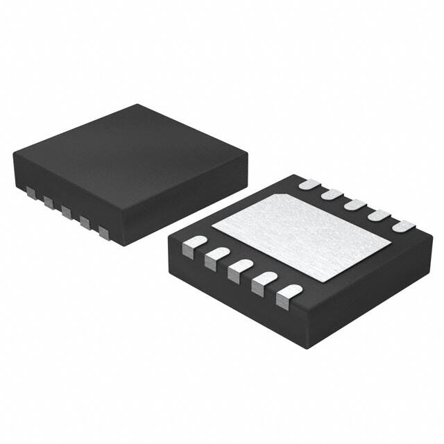
0
登录后你可以
  • 下载海量资料
  • 学习在线课程
  • 观看技术视频
  • 写文章/发帖/加入社区
会员中心
创作中心
发布
  • 发文章

  • 发资料

  • 发帖

  • 提问

  • 发视频

创作活动
MP5010BDQ-LF-P

MP5010BDQ-LF-P

  • 厂商:

    MPS(美国芯源)

  • 封装:

    VFDFN10

  • 描述:

    IC PWR SWITCH N-CHAN 1:1 10QFN

  • 数据手册
  • 价格&库存
MP5010BDQ-LF-P 数据手册
MP5010B 3V-18V, 1A-5A Programmable-CurrentLimit Switch with Over-Voltage Clamp The Future of Analog IC Technology DESCRIPTION FEATURES The MP5010B is a protection device designed to protect circuitry on the output (source) from transients on the input (VCC). It also protects the input from undesired shorts and transients coming from the source. A small capacitor on the dv/dt pin controls the slew rate that limit the inrush current at the source. For instance, a 1nF capacitor results in a source ramp-up time of 3ms. The maximum load at the source is current limited using a sense FET topology. An external resistor between the I-Limit pin and the Source pins controls the magnitude of the current limit. An internal charge pump drives the gate of the power device, allowing the DMOS power FET to have a very low ON-resistance of just 40mΩ. The MP5010B also protects the source from the input being too low or too high. Under-voltage lockout ensures that the input remains above the minimum operating threshold before the power device turns on. If the input rises above the high output threshold, the MP5010B limits the source voltage. • • • • • • • Wide 3V-to-18V Operating Input Range 5.7V Output Over-Voltage Clamp Integrated 40mΩ Power FET Enable/Fault Pin Adjustable Output Voltage Slew Rate Adjustable Current Limit Thermal Protection APPLICATIONS • • • • Hot-Swappable Devices Wireless Modem Data Cards PC Cards Laptops All MPS parts are lead-free and adhere to the RoHS directive. For MPS green status, please visit MPS website under Products, Quality Assurance page. “MPS” and “The Future of Analog IC Technology” are Registered Trademarks of Monolithic Power Systems, Inc. TYPICAL APPLICATION VIN 6 7 EN 8 9 10 11 VCC N/C I-Limit Source Source MP5010B 5 4 VOUT 3 Enable/Fault Source dv/dt Source GND Source 1 2 MP5010B Rev. 1.0 www.MonolithicPower.com 9/1/2014 MPS Proprietary Information. Patent Protected. Unauthorized Photocopy and Duplication Prohibited. © 2012 MPS. All Rights Reserved. 1 MP5010B – 3V-18V, 1A-5A PROGRAMMABLE CURRENT LIMIT SWITCH ORDERING INFORMATION Part Number* MP5010BDQ Package QFN10 (3mm×3mm) Top Marking AFN * For Tape & Reel, add suffix –Z (e.g. MP5010BDQ–Z). For RoHS compliant packaging, add suffix –LF (e.g. MP5010BDQ-LF-Z). PACKAGE REFERENCE 1 10 2 9 3 8 4 7 5 6 ABSOLUTE MAXIMUM RATINGS (1) VCC, SOURCE, I-LIMIT ..................–0.3V to 22V dv/dt, ENABLE/FAULT ....................–0.3V to 6V Storage Temperature.............. –65°C to +155°C Junction Temperature................................ +150°C Lead Temperature .................................... +260°C (2) Continuous Power Dissipation (TA=+25°C) ................................................................... 2.5W Recommended Operating Conditions (3) Input Voltage Operating Range ......... 3V to 18V Operating Junction Temp. (TJ)...... -40°C to +125°C Thermal Resistance (4) θJA θJC QFN10 (3mmx3mm) ...............50 ...... 12 ... °C/W Notes: 1) Exceeding these ratings may damage the device. 2) The maximum allowable power dissipation is a function of the maximum junction temperature TJ(MAX) , the junction-toambient thermal resistance θJA,and the ambient temperature TA, the maximum allowable power dissipation at any ambient temperature is calculated using: PD(MAX)=(TJ(MAX)-TA)/ θJA. Exceeding the maximum allowable power dissipation will cause excessive die temperature, and the regulator will go into thermal shutdown. Internal thermal shutdown circuitry protects the device from permanent damage. o Reduce 0.2 Watts for every 10 C ambient temperature increasing 3) The device is not guaranteed to function outside of its operating conditions. 4) Measured on JESD51-7 4-layer board. MP5010B Rev. 1.0 www.MonolithicPower.com 9/1/2014 MPS Proprietary Information. Patent Protected. Unauthorized Photocopy and Duplication Prohibited. © 2012 MPS. All Rights Reserved. 2 MP5010B – 3V-18V, 1A-5A PROGRAMMABLE CURRENT LIMIT SWITCH ELECTRICAL CHARACTERISTICS VCC = 5V, RLIMIT=22Ω, Capacitive Load= 10μF, TA=25°C, unless otherwise noted. Parameters Power FET Symbol Delay Time τDLY ON Resistance RDSon OFF-State Output Voltage VOFF Continuous Current Thermal Latch Shutdown Temperature(5) Under/Over-Voltage Protection Output Clamp Voltage ID Condition Min Enabling of chip to ID=40mA with a 5Ω resistive load TJ=25°C TJ=85°C(5) VCC=18V, VEN=0V, RL=500Ω 40 52 0.5 in2 pad, TA=25°C 4.2 minimum copper, TA=80°C 2.3 Max 44 55 5.5 Under-Voltage Lockout VUVLO 2.65 Under-Voltage Lockout (UVLO) VHYST Hysteresis (6) Current Limit (For Direct Current-Sense, refer to typical application in Figure 5) 0Ω Short Resistance, Hold Current ILIM-SS 2.2 RLIM=22Ω Trip Current ILIM-OL RLIM=22Ω Current Limit (6) (For Kelvin Sense, refer to typical application in Figure 4) 0Ω Short Resistance, 0.77 Hold Current ILIM-SS RLIM=22Ω Trip Current ILIM-OL RLIM=22Ω dv/dt Circuit Rise Time (7) τr Cdv/dt =1nF 2 Enable/Fault Low-Level Input Voltage VIL Output Disabled Thermal Fault, Output Intermediate-Level Input Voltage VI (INT) 0.82 Disabled High-Level Input Voltage VIH Output Enabled 2.5 HIGH-State Maximum Voltage VI (MAX) Pull-Up Current (Source) IIL VENABLE=0V 15 Maximum number of chips Maximum Fanout for Fault Signal for simultaneous shutdown Maximum Voltage on EN(8) VMAX mΩ mV A 175 Over-Voltage Protection VCC=8V Rising Edge Units μs 120 TSD VCLAMP Typ °C 5.7 5.9 V 2.8 2.9 V 0.15 2.8 V 3.4 4.3 1.10 A 1.43 2.18 3 1.4 4.95 25 MP5010B Rev. 1.0 www.MonolithicPower.com 9/1/2014 MPS Proprietary Information. Patent Protected. Unauthorized Photocopy and Duplication Prohibited. © 2012 MPS. All Rights Reserved. A A A 4 ms 0.5 V 1.95 V 35 V V μA 3 Units VCC V 3 MP5010B – 3V-18V, 1A-5A PROGRAMMABLE CURRENT LIMIT SWITCH ELECTRICAL CHARACTERISTICS (continued) VCC = 5V, RLIMIT=22Ω, Capacitive Load= 10μF, TA=25°C, unless otherwise noted. Parameters Total Device Symbol Condition Bias Current IBIAS Device Operational Thermal Shutdown Minimum Operating Voltage for UVLO VMIN Enable
MP5010BDQ-LF-P 价格&库存

很抱歉,暂时无法提供与“MP5010BDQ-LF-P”相匹配的价格&库存,您可以联系我们找货

免费人工找货