MP5018
5V, 1A-5A Current Limit Switch
with Reverse Current Blocking
and Output Over-voltage Clamp
The Future of Analog IC Technology
DESCRIPTION
FEATURES
The MP5018 is a protection device designed to
protect circuitry on the output from transients on
input (VCC). It also protects VCC from undesired
shorts and transients coming from the output.
•
At startup, inrush current is limited by the slew
rate at the output. The slew rate is controlled by
a small capacitor at the SS pin. Floating the SS
pin provides 13ms soft-start time.
•
•
•
•
•
The maximum load at the output is current
limited. The magnitude of the current limit is
controlled by an external resistor from ILIMIT to
GND. Floating ILIMIT pin provides 3A fixed
current limit. By controlling the gate voltage of a
pair of N-channel MOSFETs, any current
flowing from output to input is blocked.
Under Voltage Lockout (UVLO) assures that
input is above the minimum operating threshold,
before the power device is turned on. If input
voltage goes above 5.8V, the output voltage will
be limited at 5.8V with fast response.
The EN/Fault pin is a bi-directional, three-level
I/O with a weak pull-up. It can be used to
enable or disable MP5018, or indicate a fault
condition.
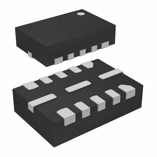
The device is available in a QFN12 (2mmx3mm)
package.
•
•
•
•
•
•
•
SAS Disable to support DEVSLP or
POWER_DOWN
4.5V to 5.5V Continued Operating Input
Range
16V Absolute Maximum Input Voltage
5.8V Fast OVP Response
Reverse Current Blocking
Integrated 45mΩ Power FET
Adjustable Current-Limit or Fixed Current
Limit when floating ILIMIT pin
210μA Typical Low Quiescent Current
Adjustable Soft Start time
Fault Indication
Latch-off Thermal Protection
Available in QFN12(2mmx3mm) Package
ESD Compliant to 2kV HBM and 1kV
CDM
APPLICATIONS
•
•
•
•
•
•
HDD, SSD
Hot Swap Systems
Gaming
Set-top Boxes/Smart TV
PCIe Cards
Switches/Routers
All MPS parts are lead-free and adhere to the RoHS directive. For MPS green
status, please visit MPS website under Products, Quality Assurance page.
“MPS” and “The Future of Analog IC Technology” are registered trademarks of
Monolithic Power Systems, Inc.
TYPICAL APPLICATION
MP5018 Rev. 1.02
3/23/2016
www.MonolithicPower.com
MPS Proprietary Information. Patent Protected. Unauthorized Photocopy and Duplication Prohibited.
© 2016 MPS. All Rights Reserved.
1
�MP5018 –5V, 1A-5A CURRENT LIMIT SWITCH WITH REVERSE CURRENT BLOCKING
AND OUTPUT OVER-VOLTAGE CLAMP
ORDERING INFORMATION
Part Number*
MP5018GD
Package
QFN-12 (2mmx3mm)
Top Marking
See Below
* For Tape & Reel, add suffix –Z (e.g. MP5018GD–Z);
TOP MARKING
AMA: product code of MP5018GD;
Y: year code;
LLL: lot number;
PACKAGE REFERENCE
QFN-12 (2mmx3mm)
ABSOLUTE MAXIMUM RATINGS (1)
Thermal Resistance
VIN ...................................................-0.3V to 16V
VOUT ............................................................. 6.3V
All Other Pins .................................–0.3V to +6V
Junction Temperature .............. -40°C to +150°C
Lead Temperature ....................................260°C
Continuous Power Dissipation (TA=+25°C )(2)
QFN-12 (2mmx3mm) ................................. 1.8W
QFN-12 (2mmx3mm).............…70........15 °C/W
Recommended Operating Conditions
(3)
Continued Operation VIN .................4.5V to 5.5V
Operating Junction Temp. (TJ). -40°C to +125°C
MP5018 Rev. 1.02
3/23/2016
(4)
θJA
θJC
Notes:
1) Exceeding these ratings may damage the device.
2) The maximum allowable power dissipation is a function of the
maximum junction temperature TJ (MAX), the junction-toambient thermal resistance θJA, and the ambient temperature
TA. The maximum allowable continuous power dissipation at
any ambient temperature is calculated by PD (MAX) = (TJ
(MAX)-TA)/θJA. Exceeding the maximum allowable power
dissipation will cause excessive die temperature, and the
regulator will go into thermal shutdown. Internal thermal
shutdown circuitry protects the device from permanent
damage.
3) The device is not guaranteed to function outside of its
operating conditions.
4) Measured on JESD51-7, 4-layer PCB.
www.MonolithicPower.com
MPS Proprietary Information. Patent Protected. Unauthorized Photocopy and Duplication Prohibited.
© 2016 MPS. All Rights Reserved.
2
�MP5018 –5V, 1A-5A CURRENT LIMIT SWITCH WITH REVERSE CURRENT BLOCKING
AND OUTPUT OVER-VOLTAGE CLAMP
ELECTRICAL CHARACTERISTICS
VIN = 5V, TJ =25°C, unless otherwise noted.
Parameter
Symbol Condition
Min
Typ
Max
Units
EN=1, SAS=0, ILoad=0
Fault latch off
EN=0, SAS=0 (or Float)
SAS=1
210
170
250
μA
μA
μA
μA
45
54
Supply Current
Quiescent Current
IQ
50
5
Power FET
ON Resistance
ON Resistance(5)
RDSon
RDSon
Turn-on Delay
Tdelay
Off-State Leakage Current
IOFF
TJ=25°C
TJ=80°C
EN=2.5V to ID=100mA with 1A
load resistor
VIN=12V, EN=0V
tSS
ISS
SS pin float, VOUT=0%-100%
Short SS to GND or add SS cap
10.4
Float ILIMIT pin
Rset=499Ω
Rset=1.4kΩ
Float ILIMIT pin
ILIMIT=3A, add 1Ω load resistor
58
500
mΩ
mΩ
μs
1
μA
13
6.5
15.6
ms
μA
2.5
1.8
0.5
3
2.3
0.8
3
3.5
2.7
1.1
A
A
A
A
5.5
10
40
μs
Soft Start
SS Time
SS Current
Current Limit
Current Limit at Normal
Operation
Short Circuit Current Limit(5)
Current Limit Response
Time(5)
Secondary Current Limit(6)
ILimit_NO
ILimit_SC
tCL
ILimitH
Any value of RISET
VUVLO
UVLO Rising Threshold
12
A
Under Voltage Protection
Under Voltage Lockout
Threshold
UVLO Hysteresis
Under Voltage Response(5)
3.8
VUVLOHYS
tUV
4.0
4.2
300
2
V
mV
μs
Reverse Current Limit
Reverse Current Limit
Reverse Current Limit
Response Time(5)
Over Voltage Protection
Over Voltage Clamp Voltage
MP5018 Rev. 1.02
3/23/2016
IReverseH
tSC
VOVLO
Latch off and pull EN to mid
level voltage
Vin dv/dt = -5V/1mS
0.9
1.2
1.5
A
5
7
10
μs
5.5
5.8
6.1
V
www.MonolithicPower.com
MPS Proprietary Information. Patent Protected. Unauthorized Photocopy and Duplication Prohibited.
© 2016 MPS. All Rights Reserved.
3
�MP5018 –5V, 1A-5A CURRENT LIMIT SWITCH WITH REVERSE CURRENT BLOCKING
AND OUTPUT OVER-VOLTAGE CLAMP
ELECTRICAL CHARACTERISTICS (continued)
VIN = 5V, TJ =25°C, unless otherwise noted.
Parameter
Over Voltage Response
Time(5)
Symbol Condition
tOV
Cout=20uF, VIN=5V to 12V
tSTD
Latched off until Enable = 0,
SAS = 1, POR
Min
Typ
Max
Units
10
40
μs
175
200
°C
0.8
V
1.95
V
3.3
5.2
-20
1
V
V
μA
μA
3
Units
0.7
V
V
V
kΩ
μs
Thermal Shutdown
Shutdown Temperature(5)
130
Enable/Fault
Low Level Input Voltage
Intermediate Level Input
Voltage
High Level Input Voltage
Maximum High State
Logic Low Sink Current
Logic Level High Current
VIL
VI (INT)
VIH
VENH
IEH_PL
IH
Maximum Fanout for Fault
Signal
UVLO, SAS Disable
Thermal fault, fast reverse
current limit
Output Enabled
0.35
0.9
1.3
2.1
3.4
EN=0V
EN = 3.3V
Total number of chips that
can be connected for
simultaneous shutdown
-12
SAS Disable
Low Level Input Voltage
High Level Input Voltage
Maximum pin voltage
Input Impedance
Deglitch Filter
VENN_L EN=1, Output enabled
VENN_H Output Disabled, EN=low
SASHmax
RENN
To GND
tSASDG
0.35
2.1
350
2
700
3.3
1000
50
Notes:
5) Guarantee by characterization test.
6) Guarantee by design.
MP5018 Rev. 1.02
3/23/2016
www.MonolithicPower.com
MPS Proprietary Information. Patent Protected. Unauthorized Photocopy and Duplication Prohibited.
© 2016 MPS. All Rights Reserved.
4
�MP5018 –5V, 1A-5A CURRENT LIMIT SWITCH WITH REVERSE CURRENT BLOCKING
AND OUTPUT OVER-VOLTAGE CLAMP
TYPICAL PERFORMANCE CHARACTERISTICS
VIN=5V, VEN=5V, ILIMIT Pin Float, SS Pin Float, SAS Pin Float, COUT=22μF, TA=25°C, unless
otherwise noted.
300
4.5
6
5
285
4
270
4
3.5
255
3
2
225
2.5
1
0
240
3
0
200 400 600 800 1000 1200
52
2
210
4
4.3
4.6
4.9
5.2
5.5
55
4.2
4.7
5.2
5.7
6.2
6.7
2
2.5
140
120
52
46
195
3.7
100
49
80
40
60
46
34
40
43
20
28
3.9
4.4
MP5018 Rev. 1.02
3/23/2016
4.9
5.4
5.9
6.4
40
4
4.3
4.6
4.9
5.2
5.5
0
0
0.5
1
www.MonolithicPower.com
MPS Proprietary Information. Patent Protected. Unauthorized Photocopy and Duplication Prohibited.
© 2016 MPS. All Rights Reserved.
1.5
5
�MP5018 –5V, 1A-5A CURRENT LIMIT SWITCH WITH REVERSE CURRENT BLOCKING
AND OUTPUT OVER-VOLTAGE CLAMP
TYPICAL PERFORMANCE CHARACTERISTICS (continued)
VIN=5V, VEN=5V, ILIMIT Pin Float, SS Pin Float, SAS Pin Float, COUT=22μF, TA=25°C, unless
otherwise noted.
MP5018 Rev. 1.02
3/23/2016
www.MonolithicPower.com
MPS Proprietary Information. Patent Protected. Unauthorized Photocopy and Duplication Prohibited.
© 2016 MPS. All Rights Reserved.
6
�MP5018 –5V, 1A-5A CURRENT LIMIT SWITCH WITH REVERSE CURRENT BLOCKING
AND OUTPUT OVER-VOLTAGE CLAMP
TYPICAL PERFORMANCE CHARACTERISTICS (continued)
VIN=5V, VEN=5V, ILIMIT Pin Float, SS Pin Float, SAS Pin Float, COUT=22μF, TA=25°C, unless
otherwise noted.
MP5018 Rev. 1.02
3/23/2016
www.MonolithicPower.com
MPS Proprietary Information. Patent Protected. Unauthorized Photocopy and Duplication Prohibited.
© 2016 MPS. All Rights Reserved.
7
�MP5018 –5V, 1A-5A CURRENT LIMIT SWITCH WITH REVERSE CURRENT BLOCKING
AND OUTPUT OVER-VOLTAGE CLAMP
TYPICAL PERFORMANCE CHARACTERISTICS (continued)
VIN=5V, VEN=5V, ILIMIT Pin Float, SS Pin Float, SAS Pin Float, COUT=22μF, TA=25°C, unless
otherwise noted.
MP5018 Rev. 1.02
3/23/2016
www.MonolithicPower.com
MPS Proprietary Information. Patent Protected. Unauthorized Photocopy and Duplication Prohibited.
© 2016 MPS. All Rights Reserved.
8
�MP5018 –5V, 1A-5A CURRENT LIMIT SWITCH WITH REVERSE CURRENT BLOCKING
AND OUTPUT OVER-VOLTAGE CLAMP
PIN FUNCTIONS
Pin #
Name
1, 2, 3
VCC
Supply Voltage. The MP5018 support 4.5V to 5.5V continuous input voltage and up to
16V maximum transient input voltage. Requires ceramic capacitor to decouple the input
rail. Connect using a wide PCB trace.
4
SAS
SAS=low to enable the part. SAS=high to disable the part. SAS pin has internal 700kΩ
pull-down resistor to ground, so it can automatically start up when SAS is floating.
5
Description
The EN/FAULT pin is a tri-state, bi-directional interface. It can be used to enable the
output of the device by floating the pin, or disable the chip by pulling it to ground (using
an open drain or open collector device). If a thermal fault occurs or reverse current limit
EN/FAULT is triggered, the voltage on this pin will go to an intermediate state to signal a monitoring
circuit that there is a device fault. When UVLO or SAS disable = 1, the voltage on this pin
will go to a low state. It can also be connected to another device in this family to cause a
simultaneous shutdown.
6
NC
7
SS
8
ILIMIT
9, 10,
11
VOUT
The output voltage that is controlled by the IC.
12, Pad
GND
System Ground.
MP5018 Rev. 1.02
3/23/2016
No Connection.
Soft start pin. Connect a capacitor from SS to ground to set the soft start time. Floating
this pin provides 13ms soft start time.
Current Limit Set pin. Place a resistor between this pin and ground to set the value of the
current limit. Floating this pin provides 3A fixed current limit.
www.MonolithicPower.com
MPS Proprietary Information. Patent Protected. Unauthorized Photocopy and Duplication Prohibited.
© 2016 MPS. All Rights Reserved.
9
�MP5018 –5V, 1A-5A CURRENT LIMIT SWITCH WITH REVERSE CURRENT BLOCKING
AND OUTPUT OVER-VOLTAGE CLAMP
FUNCTIONAL BLOCK DIAGRAM
VCC
Charge
Pump
LDO
Current
Sense
X10
VDD
Fast Off Comp
VOUT
Reverse
Comp
ILIMIT
1V
Current Limit Amp
Logic for
ILIMIT floating
Ref
Soft Start
VOUT
VDD
5V
UVLO
Control Logic
6.5uA
OVP
1.23V
EN/FAULT
SS
FLT
VDD
4uA
Thermal
Sense
SAS
0.7MΩ
Logic
8uA
13ms
80KΩ
GND
Figure 1: Functional Block Diagram
MP5018 Rev. 1.02
3/23/2016
www.MonolithicPower.com
MPS Proprietary Information. Patent Protected. Unauthorized Photocopy and Duplication Prohibited.
© 2016 MPS. All Rights Reserved.
10
�MP5018 –5V, 1A-5A CURRENT LIMIT SWITCH WITH REVERSE CURRENT BLOCKING
AND OUTPUT OVER-VOLTAGE CLAMP
OPERATION
The MP5018 is designed to limit the inrush
current to the load when a circuit card inserts
into a live backplane power source, thereby
limiting the backplane’s voltage drop and the
dV/dt of the voltage to the load as well. It offers
an integrated solution to monitor the input
voltage, output voltage, output current, and die
temperature which eliminates the requirement
of external current sense power resistor, power
MOSFET and thermal sense device.
regulated from 5V to around 1V. The typical
response time is about 10µs, during this period
the output current may have a small overshoot.
Under-Voltage Lockout (UVLO)
The MP5018 integrates a pair of back-to-back
N channel MOSFETs for reverse current
protection. Once the reverse current limit
threshold (-1.2A) is reached and exceed 7μs
deglitch time, the internal circuit will shutdown
the pair of MOSFETs. Meanwhile, the EN/Fault
line is driven to middle level; reverse current is
totally blocked and this state continues until
VCC > VOUT-2mV. When VCC >VOUT-2mV,
part resumes normal operation with soft-start
control. Whenever the input voltage drops
below UVLO threshold, back-to-back MOSFETs
are turned off and the part is shut down;
therefore, there is no reverse current during this
condition.
If the supply voltage is below the UVLO
threshold, the output is disabled, and the
EN/Fault line is driven low. When the supply
goes above the UVLO threshold, the output is
enabled and the EN/Fault is pulled high.
The nominal input supply voltage is 5V but
there are high energy transients during normal
operation or during hot swap. Those transients
depend on the parasitic inductance and
resistance of the wire along with capacitor at
VCC node. If power clamp (TVS, Tranzorb)
diode is not used, E-Fuse must be able to
withstand this transient voltage. MP5018
integrates high voltage MOSFET up to 16V and
also uses high voltage circuit for VCC node to
guarantee safe operation.
Fast Output over Voltage Clamp (OVP)
To protect the downstream loading when there
is a surge voltage at input, MP5018 provides an
accurate and fast comparator to monitor the
over voltage condition of output. If the output
voltage rises above the threshold (5.8V), the
gate of internal MOSFETs is quickly pulled
down and it’s regulated to a certain value to
maintain the output voltage clamped at 5.8V.
The fast loop response speed (10µs typical)
keeps the over voltage overshoot small.
Current Limit
The MP5018 provides a constant current limit
and the current limit can be programmed by
external resistor. Once the current limit
threshold is reached, the internal circuit will
regulate gate voltage to hold the current in
power FET constantly. In order to limit the
current, the gate to source voltage needs to be
MP5018 Rev. 1.02
3/23/2016
The desired current limit is a function of the
external current limit resistor.
MP5018 allows ILIMIT pin floating operation. If
ILIMIT pin is floating, the current limit will be set
as fixed 3A internally.
Reverse Current Blocking
Short Circuit Protection
If the load current increases rapidly due to short
circuit event, the current may exceed the
current limit threshold before control loop able
to respond. If the current reaches 12A
secondary current limit level, there is a fast turn
off circuit active to turn off the power FET with
100mA pull-down gate discharge current, as
shown in Figure 1. This can help to limit the
peak current through the switch, thus keep the
input voltage not drop too much. The total short
circuit response time is about 1µs. After the
FET is switched off, the part will restart. During
the restart process, if the short still exist,
MP5018 will regulate the gate voltage to hold
the current at normal current limit level.
www.MonolithicPower.com
MPS Proprietary Information. Patent Protected. Unauthorized Photocopy and Duplication Prohibited.
© 2016 MPS. All Rights Reserved.
11
�MP5018 –5V, 1A-5A CURRENT LIMIT SWITCH WITH REVERSE CURRENT BLOCKING
AND OUTPUT OVER-VOLTAGE CLAMP
EN Control/Fault Indication
The EN Pin enables the part when high and
disables the part when low. Floating the EN pin
will set the part auto startup because there is
internal current source pull up EN to internal
supply. The maximum internal pull up voltage
source is about 5V. EN/Fault pin is also a bi-
directional function node. When the part
entersthermal shutdown, EN/Fault pin outputs
middle level voltage ~1.3V to indicate fault
condition occurred. When VINVOUT -2mV)
SAS Floating
High
On
N/A
SAS = Low
High
On
N/A
SAS Control
The SAS pin also can control the part startup
and shutdown. When floating this pin or pull it
low, it enables the part and disables the part
when pull high.
Soft-Start
Floating SS pin can get 13ms soft start time.
While a capacitor connected to the SS pin can
set the soft start time. A constant current source
charges the SS capacitor and results in a linear
ramping voltage on the SS pin. The output
voltage rises at a similar slew rate to the SS
voltage.
time will exceed the current limit. In this case
the rise time is controlled by the load capacitor
and the current limit.
Thermal Shutdown – Latch Off
Thermal shutdown prevents the chip from
operating at exceedingly high temperature.
When the silicon die reaches temperature that
exceeds 175°C, it shuts down the whole chip,
and drives the Enable/Fault line to the middle
(MID) level. The chip is latched off after trigger
the thermal protection and it restarts when
toggle the EN or SAS or recycle the input
supply.
The soft-start time can be calculated as follows:
t ss (ms) =
1V × Css (nF)
6.5μA
Where:
tSS=soft start time
For example, a 22nF capacitor gives a soft start
time of ~3.4ms.
If the load capacitance is extremely large, the
current required to maintain the preset soft start
MP5018 Rev. 1.02
3/23/2016
www.MonolithicPower.com
MPS Proprietary Information. Patent Protected. Unauthorized Photocopy and Duplication Prohibited.
© 2016 MPS. All Rights Reserved.
12
�MP5018 –5V, 1A-5A CURRENT LIMIT SWITCH WITH REVERSE CURRENT BLOCKING
AND OUTPUT OVER-VOLTAGE CLAMP
APPLICATION INFORMATION
Setting the Current Limit
The MP5018 current limit value should exceed
the normal maximum load current, allowing the
tolerances in the current sense value. The
current limit is a function of the external currentlimit resistor. Table 2 and Figure 2 list examples
of current limit values as a function of the
resistor value.
4. Place current limit resistor R1 close to the
ILIMIT pin.
5. Place SS capacitor C2 close to SS pin.
Note: The recommend layout is based on the typical application
circuit shown in figure 4.
GND
Table 2: Current Limit vs. Current Limit Resistor
Current Limit
Resistor (Ω)
Current Limit
(A)
1070
560
442
274
215
1
2
2.5
4
5
VOUT
GND
VCC
C3
C1
VCC
VOUT
SAS
EN
R1
C2
VCC
GND
Top Layer
GND
VOUT
Bottom Layer
Figure 3: PCB Layout
Design Example
Below is a design example following the
application
guidelines
for
the
given
specifications:
Table 3: Design Example
Figure 2: Current Limit vs. Current Limit
Resistor
PCB Layout Guide
(7)
PCB layout is benefit for better performance.
Please follow these guidelines and use Figure 3
as reference.
1. Place the high-current paths (VCC and
VOUT) close to the device using short, direct,
and wide traces.
VIN (V)
Current Limit (A)
SS Time (ms)
5
3
13
The detailed application schematic is shown in
Figure 4. The typical performance and circuit
waveforms have been shown in the Typical
Performance Characteristics section. For more
detailed device applications, please refer to the
related Evaluation Board Datasheets of
MP5018.
2. Place the input capacitors as close to the
VCC and GND pins as possible.
3. Connect the VCC and VOUT pads to large
copper to achieve better thermal performance.
MP5018 Rev. 1.02
3/23/2016
www.MonolithicPower.com
MPS Proprietary Information. Patent Protected. Unauthorized Photocopy and Duplication Prohibited.
© 2016 MPS. All Rights Reserved.
13
�MP5018 –5V, 1A-5A CURRENT LIMIT SWITCH WITH REVERSE CURRENT BLOCKING
AND OUTPUT OVER-VOLTAGE CLAMP
TYPICAL APPLICATION CIRCUITS
VIN
1
C1
10 F
Power_dn
Enable
VCC
VOUT
MP5018
10
VOUT
3
9
VCC
VOUT
2
4
VCC
SAS
ILIMIT
C3
22 F
8
7
5 EN/FAULT
SS
NC
GND
R1
(Optional )
C2
(Optional )
12, Pad
6
VOUT
11
Figure 4: 5V VIN Application
Rlimit
12V
11
C1
10 F
5
N/C
VCC
4
Cdv/dt
5V
I-Limit
Source
MP5000S
3
Enable/Fault Source
7
2
9
dv/dt
Source
1 GND
Source
1
C3
10 F
Power_dn
2
3
4
5
Vout1
6
Source
8
C2
22 F
10
11
VOUT
MP5018
10
VCC
VOUT
9
VCC
VOUT
Vout2
VCC
ILIMIT
SAS
EN/ FAULT
SS
NC
GND
6
12, Pad
C4
22 F
8
7
R1
C5
(Optional)
(Optional)
Figure 5: Simultaneous Shutdown Application
MP5018 Rev. 1.02
3/23/2016
www.MonolithicPower.com
MPS Proprietary Information. Patent Protected. Unauthorized Photocopy and Duplication Prohibited.
© 2016 MPS. All Rights Reserved.
14
�MP5018 –5V, 1A-5A CURRENT LIMIT SWITCH WITH REVERSE CURRENT BLOCKING
AND OUTPUT OVER-VOLTAGE CLAMP
PACKAGE INFORMATION
QFN-12 (2mmx3mm)
NOTICE: The information in this document is subject to change without notice. Users should warrant and guarantee that third
party Intellectual Property rights are not infringed upon when integrating MPS products into any application. MPS will not
assume any legal responsibility for any said applications.
MP5018 Rev. 1.02
3/23/2016
www.MonolithicPower.com
MPS Proprietary Information. Patent Protected. Unauthorized Photocopy and Duplication Prohibited.
© 2016 MPS. All Rights Reserved.
15
�