MP5030C
USB Charging Port Controller with
Current Limit Switch, Supporting
CDP, DCP, and QC3.0 Modes
DESCRIPTION
FEATURES
The MP5030C integrates a USB current-limit
switch and charging port identification circuit.
The MP5030C achieves 3A of continuous
output current over a wide input supply range.
The output of the USB switch is current-limit
programmable. The MP5030C
supports
dedicated charging port (DCP) and charging
downstream port (CDP) schemes for battery
charging specification (BC1.2), divider mode,
1.2V/1.2V mode, and quick-charge specification
(QC 2.0/3.0) without the need for external user
interaction.
The MP5030C provides linear
compensation for 5V outputs.
line
drop
Up to 14V Operating Input Voltage Range
Support DCP Schemes for BC 1.2 without
QC Mode, Divider Mode, and 1.2V/1.2V
Mode
Supports QC 3.0 Mode
Support CDP Mode for USB 2.0 Data
Line Drop Compensation for 5V Output
Programmable High-Accuracy Current Limit
32mΩ Low RDS(ON) Power MOSFET
Input Over-Voltage Shutdown Protection
Compatible with Buck, Boost, AC/DC
Converters
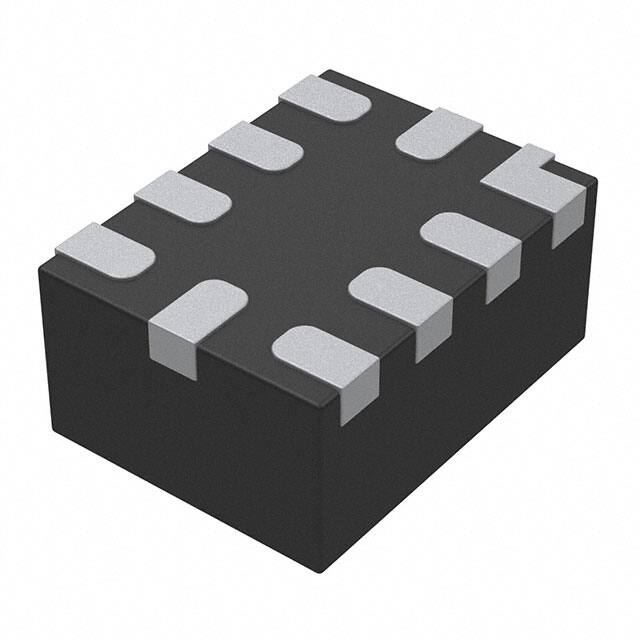
Available in a QFN-10 (1.5mmx2mm)
Package
APPLICATIONS
Full protection features include hiccup current
limiting, input over-voltage protection (OVP),
and thermal shutdown.
The MP5030C requires a minimal number of
readily
available,
standard,
external
components to complete the USB switch and
charging mode auto-detection solution. The
MP5030C is available in a QFN-10
(1.5mmx2mm) package.
USB Charging Downstream Port (CDP)
USB Dedicated Charging Ports (DCP)
All MPS parts are lead-free, halogen-free, and adhere to the RoHS
directive. For MPS green status, please visit the MPS website under
Quality Assurance. “MPS” and “The Future of Analog IC Technology” are
registered trademarks of Monolithic Power Systems, Inc.
TYPICAL APPLICATION
OUT
5V
VIN
5V
OUT
IN
C2
10μF
C5
22μF
MODE
MP5030C
DM
ADJ
DP
DP_OUT
DM_OUT
R6
1.5kΩ
ILIM
R8
1kΩ
USB
L2
Bead,2.5kΩ
100MHz
GND
To USB Host
CDP Mode Set-Up for USB2.0 Application
MP5030C Rev. 1.01
www.MonolithicPower.com
9/28/2018
MPS Proprietary Information. Patent Protected. Unauthorized Photocopy and Duplication Prohibited.
© 2018 MPS. All Rights Reserved.
1
�MP5030C – USB CHARGING PORT CONTROLLER SUPPORTING CDP, DCP, AND QC3.0
ORDERING INFORMATION
Part Number*
MP5030CGQH
Package
QFN-10 (1.5mmx2mm)
Top Marking
See Below
* For Tape & Reel, add suffix –Z (e.g. MP5030CGQH–Z)
TOP MARKING
GB: Product code of MP5030CGQH
LL: Lot number
PACKAGE REFERENCE
TOP VIEW
DP_OUT
10
DP
1
9 DM_OUT
DM
2
8
OUT
ILIM 3
7
IN
ADJ 4
6
GND
5
MODE
QFN-10 (1.5mmx2mm)
MP5030C Rev. 1.01
www.MonolithicPower.com
9/28/2018
MPS Proprietary Information. Patent Protected. Unauthorized Photocopy and Duplication Prohibited.
© 2018 MPS. All Rights Reserved.
2
�MP5030C – USB CHARGING PORT CONTROLLER SUPPORTING CDP, DCP, AND QC3.0
ABSOLUTE MAXIMUM RATINGS
(1)
Supply voltage (VIN) ..................... -0.3V to +16V
Output voltage (VIN) ..................... -0.3V to +16V
All other pins .................................. -0.3V to +6V
Junction temperature ............................... 150°C
Lead temperature .................................... 260°C
Continuous power dissipation (TA = +25°C) (2)
................................................................ 2.23W
Recommended Operating Conditions (3)
Supply voltage (VIN) ....................... Up to 14V (4)
Output voltage (VOUT) ................... follow with VIN
Output current (IOUT).............................. up to 3A
Operating junction temp. (TJ). .. -40°C to +125°C
Thermal Resistance
θJA
θJC
QFN-10 (1.5mmx2mm)
EV5030C-QH-00C ................ 56 ....... 18 ... °C/W
JESD51-7 (5) ........................ 130 ...... 25 ... °C/W
NOTES:
1) Exceeding these ratings may damage the device.
2) The maximum allowable power dissipation is a function of the
maximum junction temperature TJ (MAX), the junction-toambient thermal resistance θJA, and the ambient temperature
TA. The maximum allowable continuous power dissipation at
any ambient temperature is calculated by PD (MAX) = (TJ
(MAX)-TA)/θJA. Exceeding the maximum allowable power
dissipation produces an excessive die temperature, causing
the regulator to go into thermal shutdown. Internal thermal
shutdown circuitry protects the device from permanent
damage. Measured on EV5030C-QH-00A, 2-layer PCB,
4.4cmx2.9cm, 2Oz copper.
3) The device is not guaranteed to function outside of its
operating conditions.
4) For lower VIN applications, refer to the Operation section on
page 12.
5) Measured on JESD51-7, 4-layer PCB.
MP5030C Rev. 1.01
www.MonolithicPower.com
9/28/2018
MPS Proprietary Information. Patent Protected. Unauthorized Photocopy and Duplication Prohibited.
© 2018 MPS. All Rights Reserved.
3
�MP5030C – USB CHARGING PORT CONTROLLER SUPPORTING CDP, DCP, AND QC3.0
ELECTRICAL CHARACTERISTICS
VIN = 5V, TJ = -40°C to 125°C (6), Typical value is tested at TJ = +25°C, unless otherwise noted.
Parameter
VIN under-voltage lockout
rising threshold
UVLO hysteresis
Second VIN under-voltage
lockout rising threshold
Second UVLO hysteresis
Start-up delay
Supply current
USB Power MOSFET
On resistance
Symbol
Condition
Min
Typ
Max
Units
VIN_UVLO1
ADJ starts to work
2.7
3.0
3.3
V
VUVLOHYS1
VIN_UVLO2
880
Power MOSFET turn-on
3.7
VUVLOHYS2
TDelay
IQ
4.1
500
From UVLO rising to VOUT =
100mV
VIN = 5V, no load
4
V
mV
5
6
ms
250
320
μA
32
50
mΩ
Input discharge resistance
RDIS
Soft-start time
Current Limit Set
TSS
VIN = 5V
Turn-on during VIN OVP or H to L
voltage change period
VIN = 5V, no load, 10% to 90%
USB current limit
Output Voltage Control
ILIMIT
RILIM = 1.5kΩ, VOUT drops 10%
3.13
3.35
3.57
A
VIN_Def1
VIN_Def2
VIN_9
VIN_12
Isink
VIN_5_C
IOUT = 0A, TJ = +25°C
TJ = -40°C to +125°C
TJ = +25°C
TJ = +25°C
VFB = 800mV
IOUT = 2.4A, only 5VIN active
-1%
-2%
-2%
-2%
500
5
5
9
12
+1%
+2%
+2%
+2%
V
220
350
V
V
μA
mV
VOV_TH
VIN rising edge, VIN = 5V
VIN rising edge, VIN = 9V
110
110
115
115
120
120
%
VIN rising edge, VIN = 12V
110
115
120
Reset mode to 5V default
5.25
5.4
10
5.55
Default VIN
9VIN voltage
12VIN voltage
VADJ sink current capability
Line drop compensation
Protection
VIN OVP threshold
VIN OVP recovery
OVP deglitch time (7)
RDSON
3.9
mV
VOV_Recovery
TOVP_DE
72
Ω
290
µs
V
μs
OCP on time of hiccup
THIC_ON
2
ms
OCP off time of hiccup
Shutdown temperature (7)
Hysteresis (7)
MODE Selection
THIC_OFF
TSTD
THYS
2
160
35
s
°C
°C
MODE voltage
VMODE
MODE = high, DCP mode with
QC function
2.1
MODE = float, DCP mode without
QC function
0.9
MODE = low, CDP mode
MP5030C Rev. 1.01
www.MonolithicPower.com
9/28/2018
MPS Proprietary Information. Patent Protected. Unauthorized Photocopy and Duplication Prohibited.
© 2018 MPS. All Rights Reserved.
1.9
V
0.5
4
�MP5030C – USB CHARGING PORT CONTROLLER SUPPORTING CDP, DCP, AND QC3.0
ELECTRICAL CHARACTERISTICS (continued)
VIN = 5V, TJ = -40°C to 125°C (6), Typical value is tested at TJ = +25°C, unless otherwise noted.
Parameter
BC 1.2 DCP Mode
DP/DM short resistance
Symbol
RDP/DM_Short
Condition
Min
Typ
VDP = 0.8V, IDM = 1mA, TJ =
+25°C
Max
Units
50
Ω
1.2V/1.2V Mode
DP/DM output voltage
DP/DM output impedance
Divider Mode
VDP/DM_1.2V
RDP/DM_1.2V
DP/DM output voltage
DP/DM output impendence
Quick Charge 3.0 Mode
VDP/DM
RDP/DM
VIN = VOUT = 5V
1.1
1.2
300
1.3
V
kΩ
2.5
18
2.7
22
2.85
28
V
kΩ
Data detect voltage
VDAT_REF
0.25
0.3
0.4
V
Output voltage select ref
DP output impendence
DM output impendence
DM low glitch time
DP high glitch time
Output voltage change
glitch time
VBUS voltage step
CDP Mode
VSEL_REF
RDP_QC
RDM_QC
TGlitch_DM
TGlitch_DP
1.8
250
15
2
350
20
10
2.2
450
25
1000
1500
V
kΩ
kΩ
ms
ms
TGlitch_V_Change
20
40
60
ms
Vstep
150
200
250
mV
0.5
0.6
0.7
V
0.25
0.3
0.4
V
DM CDP output voltage
VDM_SRC
VDP = 0.6V
DP rising lower window
threshold for VDM_SRC
VDAT_RE
activation
DP rising lower window
threshold hysteresis for
VDAT_RE_HYS
VDM_SRC activation
DP rising upper window
threshold for VDM_SRC deVLGC_SRC
activation
DP rising upper window
threshold hysteresis for
VLGC_SRC_HYS
VDM_SRC de-activation
VDM_SRC on/off deglitch time VDM_SRC_Deglitch
RDP_Down, RDM_Down
RDP/DM_Down
DP/DM switch on
RON_DP/DM
resistance
DP to DP_OUT SW on cap
CDP
Same for DM switch
(7)
3dB bandwidth of analog
data SW (7)
FBW
50
1.9
mV
2
200
3.8
14.25
4.8
19.5
2.5
5.3
500
V
mV
5.8
24.8
ms
kΩ
Ω
pF
MHz
NOTES:
6) Guaranteed by over-temperature correlation, not tested in production.
7) Guaranteed by engineering sample characterization.
MP5030C Rev. 1.01
www.MonolithicPower.com
9/28/2018
MPS Proprietary Information. Patent Protected. Unauthorized Photocopy and Duplication Prohibited.
© 2018 MPS. All Rights Reserved.
5
�MP5030C – USB CHARGING PORT CONTROLLER SUPPORTING CDP, DCP, AND QC3.0
TYPICAL CHARACTERISTICS
VIN = 5V, VOUT = 5V, RILIM = 1.5kΩ, TA = 25°C, unless otherwise noted.
Quiescent Current vs. Temperature
44
42
40
38
36
34
32
30
28
26
24
400
QUIESCENT CURRENT (μA)
RDSON (mΩ)
RDS(ON) vs. Input Voltage
3
4
5
6
7
8
9 10
INPUT VOLTAGE (V)
11
350
300
250
200
150
100
50
0
-50
12
Line Drop Compensation
0
25
50
75
TEMPERATURE(°C)
100
125
Current Limit vs. RLIMIT
300
4.5
4
250
CURRENT LIMIT(A)
LINE DROP
COMPENSATION (mV)
-25
200
150
100
50
3.5
3
2.5
2
1.5
1
0.5
MODE=high/low/float
0
0
0
0.5
1
1.5
2
2.5
OUTPUT CURRENT (A)
3
1 1.5 2 2.5 3 3.5 4 4.5 5 5.5 6
RLIMIT (kΩ)
MP5030C Rev. 1.01
www.MonolithicPower.com
9/28/2018
MPS Proprietary Information. Patent Protected. Unauthorized Photocopy and Duplication Prohibited.
© 2018 MPS. All Rights Reserved.
6
�MP5030C – USB CHARGING PORT CONTROLLER SUPPORTING CDP, DCP, AND QC3.0
TYPICAL PERFORMANCE CHARACTERISTICS (continued)
VIN = 5V, VOUT = 5V, RILIM = 1.5kΩ, TA = 25°C, unless otherwise noted. Connect the MP5030C input
to the MP2499A output. System_VIN is the MP2499A input voltage.
Start-Up through Input Voltage
Shutdown through Input Voltage
IOUT = 0A
IOUT = 0A
CH1: VOUT
2V/div.
CH1: VOUT
2V/div.
CH2:
VIN/MP5030C
5V/div.
CH2:
VIN/MP5030C
5V/div.
CH3:
System_VIN
CH3:
System_VIN
10V/div.
CH4: IOUT
1A/div.
10V/div.
CH4: IOUT
2A/div.
5ms/div.
20ms/div.
Mode Transition from 5V to 9V
Mode Transition from 5V to 9V
IOUT = 0A, from QC 2.0_5V to 9V
Zoom in 5V to 9V slew rate
CH1: VOUT
5V/div.
CH1: VOUT
5V/div.
CH2: DP
2V/div.
CH2: DP
2V/div.
CH3: DM
2V/div.
CH4: IOUT
500mA/div.
CH3: DM
2V/div.
CH4: IOUT
500mA/div.
10ms/div.
500µs/div.
Mode Transition from 9V to 12V
Mode Transition from 9V to 12V
IOUT = 0A, from QC 2.0_9V to 12V
Zoom in 9V to 12V slew rate
CH1: VOUT
5V/div.
CH2: DP
2V/div.
CH1: VOUT
5V/div.
CH2: DP
2V/div.
CH3: DM
2V/div.
CH4: IOUT
500mA/div.
CH3: DM
2V/div.
CH4: IOUT
500mA/div.
10ms/div.
500µs/div.
MP5030C Rev. 1.01
www.MonolithicPower.com
9/28/2018
MPS Proprietary Information. Patent Protected. Unauthorized Photocopy and Duplication Prohibited.
© 2018 MPS. All Rights Reserved.
7
�MP5030C – USB CHARGING PORT CONTROLLER SUPPORTING CDP, DCP, AND QC3.0
TYPICAL PERFORMANCE CHARACTERISTICS (continued)
VIN = 5V, VOUT = 5V, RILIM = 1.5kΩ, TA = 25°C, unless otherwise noted. Connect the MP5030C input
to the MP2499A output. System_VIN is the MP2499A input voltage.
Mode Transition from 12V to 9V
Mode Transition from 9V to 5V
IOUT = 0A, from QC 2.0_12V to 9V
IOUT = 0A, from QC 2.0_9V to 5V
CH1: VOUT
5V/div.
CH1: VOUT
5V/div.
CH2: DP
2V/div.
CH2: DP
2V/div.
CH3: DM
2V/div.
CH4: IOUT
500mA/div.
CH3: DM
2V/div.
CH4: IOUT
500mA/div.
10ms/div.
10ms/div.
Input Over-Voltage Protection
Input Over-Voltage Protection
QC 5V Mode, IOUT = 0A
QC 9V Mode, IOUT = 0A
CH1: VOUT
2V/div.
CH2:
VIN/MP5030C
2V/div.
CH1: VOUT
5V/div.
CH2:
VIN/MP5030C
5V/div.
CH4: IOUT
2A/div.
CH4: IOUT
2A/div.
1s/div.
2s/div.
Short-Circuit Protection Entry
and Recovery
Short-Circuit Protection Entry
and Recovery
VIN = 5V, IOUT = 0A
VIN = 9V, IOUT = 0A
CH1: VOUT
2V/div.
CH2:
VIN/MP5030C
2V/div.
CH1: VOUT
5V/div.
CH2:
VIN/MP5030C
5V/div.
CH4: IOUT
2A/div.
CH4: IOUT
2A/div.
2s/div.
2s/div.
MP5030C Rev. 1.01
www.MonolithicPower.com
9/28/2018
MPS Proprietary Information. Patent Protected. Unauthorized Photocopy and Duplication Prohibited.
© 2018 MPS. All Rights Reserved.
8
�MP5030C – USB CHARGING PORT CONTROLLER SUPPORTING CDP, DCP, AND QC3.0
TYPICAL PERFORMANCE CHARACTERISTICS (continued)
VIN = 5V, VOUT = 5V, RILIM = 1.5kΩ, TA = 25°C, unless otherwise noted. Connect the MP5030C input
to the MP2499A output. System_VIN is the MP2499A input voltage.
QC 3.0 Device Charging Test
CDP Mode Detection
Mobile phone plug-in
CH1: VOUT
5V/div.
CH1: VOUT
5V/div.
CH2: DP
2V/div.
CH2: DM
1V/div.
CH3: DM
2V/div.
CH4: ICHARGE
1A/div.
CH3: DP
1V/div.
CH4:
ICHARGE
1A/div.
2s/div.
200ms/div.
Eye Pattern Test
Recommended CDP mode set-up
MP5030C Rev. 1.01
www.MonolithicPower.com
9/28/2018
MPS Proprietary Information. Patent Protected. Unauthorized Photocopy and Duplication Prohibited.
© 2018 MPS. All Rights Reserved.
9
�MP5030C – USB CHARGING PORT CONTROLLER SUPPORTING CDP, DCP, AND QC3.0
PIN FUNCTIONS
Package
Pin #
Name
1
DP
2
DM
3
ILIM
4
ADJ
5
MODE
6
7
8
9
GND
IN
OUT
DM_OUT
D+ data line to USB connector. DP is the input/output used for handshaking with
portable devices.
D- data line to USB connector. DM is the input/output used for handshaking with
portable devices.
Set the current limit level. Place a resistor between ILIM and GND to achieve a
high-accuracy current limit.
Output voltage adjustment. ADJ sinks a current from the upstream DC/DC
converter's FB pin to ground to regulate the DC/DC converter's output voltage. ADJ
also supports line drop compensation.
USB mode control. Float MODE to operate the USB in DCP mode without the QC
function. Pull MODE high to operate the USB in DCP mode with the QC function.
Pull MODE low to operate the USB in CDP mode. MODE has a 1MΩ pull-up resistor
to an internal +1.2V source.
Ground.
Supply voltage.
Output of the USB current limit switch.
D- data line to the USB host controller.
10
DP_OUT
D+ data line to the USB host controller.
Description
MP5030C Rev. 1.01
www.MonolithicPower.com
9/28/2018
MPS Proprietary Information. Patent Protected. Unauthorized Photocopy and Duplication Prohibited.
© 2018 MPS. All Rights Reserved.
10
�MP5030C – USB CHARGING PORT CONTROLLER SUPPORTING CDP, DCP, AND QC3.0
BLOCK DIAGRAM
IN
OUT
Current
Sense
Driver
Charge Pump
IN
Vin
sense
VDD Regulator
R1
Line Drop
Compensation
(5V only)
Current Limit
Protection
ILIM
DP
Auto Charging
Mode
Detection
R2
DM
Vo Reference and
Slew Rate
Σ
+1.2V
1MΩ
MODE
IN
IN
ADJ
Over Voltage
Protection
CDP
MODE
Control
Compensation
Discharge
GND
DM_OUT
DP_OUT
Figure 1: Functional Block Diagram
MP5030C Rev. 1.01
www.MonolithicPower.com
9/28/2018
MPS Proprietary Information. Patent Protected. Unauthorized Photocopy and Duplication Prohibited.
© 2018 MPS. All Rights Reserved.
11
�MP5030C – USB CHARGING PORT CONTROLLER SUPPORTING CDP, DCP, AND QC3.0
OPERATION
The MP5030C integrates a USB current-limit
switch and charging port identification circuit.
The MP5030C achieves 3A of continuous
output current over a wide input supply range.
The output of the USB switch is current-limited
with an adjustable current-limit threshold. The
MP5030C
supports
the
quick-charge
specification (QC 3.0) and is backwardscompatible with QC 2.0. The MP5030C also
supports DCP/CDP schemes for battery
charging specification (BC1.2), divider mode,
and 1.2V/1.2V mode without the need for
external user interaction.
The MP5030C provides line drop compensation
for a 5V output. Fault condition protection
includes hiccup current limiting, input overvoltage protection (OVP), and thermal
shutdown.
Operation Supply Voltage
The MP5030C has a two-stage input voltage
threshold. The first threshold is around 3V, and
the second threshold is the under-voltage
lockout (UVLO) of the power MOSFET. When
VIN is higher than the first threshold, the
MP5030C's ADJ block starts working and sinks
a current to adjust the upstream regulator's
output to an accurate 5V. Afterward, the
MP5030C enters a fully working state.
Under-Voltage Lockout (UVLO)
UVLO protects the chip from operating at an
insufficient supply voltage. The MP5030C's
second UVLO comparator monitors the input
voltage. Once the input voltage is higher than
the second UVLO threshold, the power
MOSFET starts to turn on with a controlled slew
rate after a fixed delay.
Internal Soft Start (SS)
The internal soft-start prevents the output
voltage from inrush current and overshooting
during start-up.
MODE Selection
The MP5030C supports DCP and CDP modes
through MODE control. Pull MODE high to
operate the USB in DCP mode with the QC
function. Float MODE to operate the USB in
DCP mode without the QC function. Pull MODE
low to operate the USB in CDP mode.
In DCP mode, the MP5030C can provide power
for USB devices with protocol auto-detection. It
supports the following charging schemes:
USB
battery
charging
specification
BC1.2/Chinese
Telecommunications
Industry
Standard YD/T 1591-2009
Divider mode
1.2V/1.2V mode
Quick-charge mode 2.0
Quick-charge mode 3.0 (3.6 - 12V)
For better data transmission performance in
CDP mode, use the MP5030C in USB CDP
mode for handshaking. Bypass DP to DP_OUT.
DM to DM_OUT switches internally (see Figure
2).
DM
DP
MP5030C
DM_OUT
R8, 1kΩ
L2,Bead,
2.5kΩ
@100MHz
TypeA
To HOST
Controller
DP_OUT
Figure 2: CDP Mode Set-Up
In CDP mode, the bus voltage (VBUS) is always
around 5V with current limit and line drop
compensation (see Table 1).
Table 1: MODE Selection
MODE Status
Logic high
Float
Logic low
Supported Charge Mode
DCP mode, divider mode,
QC2.0, QC3.0 mode, 1.2V/1.2V
mode
DCP mode without QC function,
divider mode, 1.2V/1.2V mode
CDP mode, 5VOUT with line drop
compensation
Connect DP and DM with a 150Ω resistor for
DCP without QC mode.
Line Drop Compensation
The MP5030C can compensate for an output
voltage drop, such as high impedance caused
by a long trace, to maintain a fairly constant 5V
load-side voltage. Line drop compensation is
achieved through ADJ. The MP5030C
increases the input voltage by 220mV at a 2.4A
output current (see Figure 3).
MP5030C Rev. 1.01
www.MonolithicPower.com
9/28/2018
MPS Proprietary Information. Patent Protected. Unauthorized Photocopy and Duplication Prohibited.
© 2018 MPS. All Rights Reserved.
12
�MP5030C – USB CHARGING PORT CONTROLLER SUPPORTING CDP, DCP, AND QC3.0
V
ΔVIN
VIN
220mV
VFB=108%*Vref
20ms
Discharge
Enable
0
2.4A
IOUT
t
Figure 3: Line Drop Compensation
VADJ sinks a controlled current slowly. The line
drop compensation amplitude increases linearly
as the load current increases.
In no-load condition, if the input voltage is lower
than 5V (typical), ADJ sinks a current to
regulate the upstream regulator's output voltage
to 5V. If the input voltage is higher than 5V
(typical), the MP5030C no longer regulates the
input voltage.
Input Over-Voltage and Discharge
To protect the downstream device from an
over-voltage condition, the MP5030C provides
an input over-voltage protection (OVP)
shutdown function. Since the MP5030C
supports the QC 3.0 protocol, it has a dynamic
OVP threshold.
An accurate and fast comparator monitors the
over-voltage condition of the input. If the input
voltage rises above the threshold, the gate of
the internal MOSFET is pulled low quickly, and
the
power
MOSFET
is
shut
down.
Simultaneously, the input-to-ground discharge
path is active. When the input voltage falls
below 5.4V (typical), the MP5030C exits OVP
mode.
The OVP shutdown function is blanked during
the high-to-low voltage mode change period.
The input-to-ground discharge resistance is
always active during the high-to-low voltage
mode change period. The discharge path is
turn-off when FB is lower than 108% times the
reference voltage (VREF) with 20ms of additional
delay (see Figure 4).
Figure 4: Input Discharge during High Voltage to
Low Voltage Transition
QC mode is reset during the OVP rising edge.
Over-Current Protection (OCP)
The MP5030C provides a constant current limit.
The current limit threshold is adjustable by an
external resistor.
Once the device reaches its current limit
threshold, the internal circuit regulates the gate
voltage to hold the current in the power
MOSFET constant.
The external resistor (RLimit) can set the current
limit threshold. If an over-current (OC) condition
occurs but VOUT is higher than 3.5V, the
MP5030C works at a constant current (CC) limit
mode without hiccup mode. If the OC is
triggered and VOUT is lower than 3.5V for 2ms,
the MP5030C enters hiccup mode. In hiccup
mode, the MP5030C turns off the power
MOSFET (see Figure 5).
THIC_ON
VOUT
THIC_OFF