0
登录后你可以
  • 下载海量资料
  • 学习在线课程
  • 观看技术视频
  • 写文章/发帖/加入社区
会员中心
创作中心
发布
  • 发文章

  • 发资料

  • 发帖

  • 提问

  • 发视频

创作活动
MP5461GC-Z

MP5461GC-Z

  • 厂商:

    MPS(美国芯源)

  • 封装:

    WLCSP12

  • 描述:

    DUAL INPUT, 4-SWITCH INTEGRATED

  • 详情介绍
  • 数据手册
  • 价格&库存
MP5461GC-Z 数据手册
MP5461 Dual Input, 4-Switch Integrated Buck-Boost Converter with Input ORing and Selection DESCRIPTION FEATURES The MP5461 is a dual input, 4-switch, integrated buck-boost converter. It is capable of regulating the output voltage from 4.2V to 5.5V VIN1 and 2.5V to 5.5V VIN2. The VIN1 can support up to 22V input voltage but is not functional after >5.75V.  The MP5461 has two auto-ORing switches from VIN1 and VIN2 to achieve a stable input for the buck-boost converter. The two sets of ORing MOSFETs are integrated. If one channel power source falls, the fast turn-off protection minimizes the reverse current. The buck-boost converter can operate from an input voltage above, equal to, or below the output voltage. It uses current-mode control with 1.8MHz fixed PWM frequency to optimize stability and transient response. In a light-load condition, it enters PFM mode to get high lightload efficiency. Integrated MOSFETs minimize the solution size while maintaining high efficiency. Fault protection includes VIN1 OVP shutdown, output hiccup current limiting, and thermal shutdown. The MP5461 is available in a tiny CSP-12 (1.4mmx1.8mm) package.        Dual Input ORing Switches: o 4.2V to 5.5V Input Voltage Range for VIN1 o Supports 22V Voltage Stress for VIN1 o 5.75V OVP Shutdown for VIN1 o 2.5V to 5.5V Input Voltage Range for VIN2 o Fast Reverse Block within 2μs o 1A Current Capability for Each Channel o Soft-Start Control o Fast SCP (Short-Circuit Protection) on OR_OUT o Power-Path Selection Input o Power-Path Status Indication Buck-Boost Converter o 1.8MHz Switching Frequency for CCM o 3.3V Fixed Output Voltage o 500mA Continuous Output Current o 1ms Soft-Start Time o Auto PFM/PWM Mode o Output Over-Voltage Protection o Hiccup Over-Current Protection 1µA Shutdown Current 200µA Quiescent Current Active Low System EN Pin EN to OR_OUT Start-Up Delay 300μs Over-Temperature Shutdown Available in a Wafer Level Chip Scale Packaging: CSP-12(1.4mmx1.8mm) APPLICATIONS   USB-C Cable VCONN Powered USB Device All MPS parts are lead-free, halogen free, and adhere to the RoHS directive. For MPS green status, please visit MPS website under Quality Assurance. “MPS” and “The Future of Analog IC Technology” are Registered Trademarks of Monolithic Power Systems, Inc. MP5461 Rev. 1.0 2/19/2019 www.MonolithicPower.com MPS Proprietary Information. Patent Protected. Unauthorized Photocopy and Duplication Prohibited. © 2019 MPS. All Rights Reserved. 1 MP5461 – DUAL INPUT, INTEGRATED BUCK-BOOST TYPICAL APPLICATION Efficiency vs. Load Current L1 1µH VIN1 4.2V-5.5V SW1 VIN2 2.5V-5.5V SW2 IN1 95 OUT C2A 22µF MP5461 C1B 1µF IN2 OR_OUT C4 10µF VCC R1 10k SEL STATUS MP5461 Rev. 1.0 2/19/2019 100 VCC EN AGND GND C2B 22µF 90 EFFICIENCY (%) C1A 1µF VOUT 3.3V/0.5A 85 80 75 VIN2=5V VIN2=3.3V VIN2=2.7V 70 65 C3 1µF 60 0.001 0.01 0.1 LOAD CURRENT (A) www.MonolithicPower.com MPS Proprietary Information. Patent Protected. Unauthorized Photocopy and Duplication Prohibited. © 2019 MPS. All Rights Reserved. 1 2 MP5461 – DUAL INPUT, INTEGRATED BUCK-BOOST ORDERING INFORMATION Part Number* Package Top Marking MP5461GC CSP-12 (1.4mmx1.8mm) See Below * For Tape & Reel, add suffix –Z (e.g. MP5461GC–Z). TOP MARKING JG: Product code of MP5461GC Y: Year code LLL: Lot number PACKAGE REFERENCE TOP VIEW 1 2 3 A IN1 OR_ OUT SW 1 B IN2 AG ND GN D C VC C EN SW 2 D SE L STAT US OU T CSP-12 (1.4mmx1.8mm) MP5461 Rev. 1.0 2/19/2019 www.MonolithicPower.com MPS Proprietary Information. Patent Protected. Unauthorized Photocopy and Duplication Prohibited. © 2019 MPS. All Rights Reserved. 3 MP5461 – DUAL INPUT, INTEGRATED BUCK-BOOST PIN FUNCTIONS CSP-12 Pin # Name A1 IN1 A2 OR_OUT A3 SW1 B1 IN2 B2 AGND B3 GND C1 VCC C2 EN C3 SW2 D1 SEL D2 STATUS D3 OUT MP5461 Rev. 1.0 2/19/2019 Description VIN1 supply voltage. The MP5461 operates from a 4.2V to 5.5V VIN1 voltage and supports a 22V input voltage, but it is not functional >5.75V. CIN1 prevents large voltage spikes at the input. Place CIN1 as close to the IC as possible. IN1, IN2 ORing output. Also functions as the buck-boost input pin. Use a 10μF or larger capacitor for decoupling. Switch1. The first half-bridge switch node is connected to SW1. Connect an inductor between SW1 and SW2. VIN2 supply voltage. The MP5461 operates from a 2.5V to 5.5V VIN2 voltage. CIN2 prevents large voltage spikes at the input. Place CIN2 as close to the IC as possible. Analog ground. Connect AGND to VCC capacitor's GND node by a Kelvin sense trace. Power ground. Reference ground of the regulated output voltage. GND requires extra care during PCB layout. Connect to GND with copper traces and vias. Internal 5V LDO regulator output. Decouple with a 1µF capacitor. On/off control for entire chip. EN is active low. Drive EN high to turn off the chip. Drive EN low or float to turn on the device. It has an internal 600kΩ pulldown resistor to ground. Switch2. The internal second half-bridge switch node is connected to SW2. Connect an inductor between SW1 and SW2. Power path select input. If SEL=Low or is floated, VIN1 is selected; If SEL=High, VIN2 is selected. The MP5461 will auto select the available power path if only one supply is available. It has an internal 600kΩ pull-down resistor to ground. Status indication. Open drain output. Indicates if the VIN1 or VIN2 channel is selected. Refer to the truth table. Output pin. www.MonolithicPower.com MPS Proprietary Information. Patent Protected. Unauthorized Photocopy and Duplication Prohibited. © 2019 MPS. All Rights Reserved. 4 MP5461 – DUAL INPUT, INTEGRATED BUCK-BOOST ABSOLUTE MAXIMUM RATINGS (1) Supply Voltage (VIN1) ....................-0.3V to +24V VSW1..................................................................... –0.3V (-5V for
MP5461GC-Z
物料型号:MP5461 器件简介:MP5461是一款双输入、4开关集成的升降压转换器,能够调节4.2V至5.5V的VIN1和2.5V至5.5V的VIN2的输出电压。它具备输入或逻辑和选择功能。 
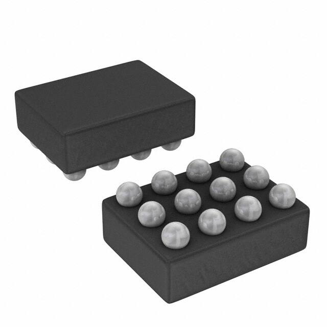
引脚分配:MP5461有12个引脚,包括输入电压引脚IN1和IN2、开关节点SW1和SW2、控制和状态引脚等。 参数特性:具有1A的电流能力、软启动控制、快速短路保护、功率路径选择输入和状态指示等功能。 功能详解:MP5461可以在输入电压高于、等于或低于输出电压的情况下工作,使用1.8MHz的固定PWM频率优化稳定性和瞬态响应。 应用信息:适用于USB-C Cable VCONN供电的USB设备等。 封装信息:提供CSP-12(1.4mmx1.8mm)封装。

特点包括: - 双输入或逻辑开关:支持22V的电压应力,具有5.75V的过压保护。 - 1µA的关闭电流和200µA的静态电流。 - 系统使能引脚EN,具有EN到OR_OUT的300μs启动延迟。 - 超温保护。 - 采用晶圆级芯片尺寸封装:CSP-12(1.4mmx1.8mm)。

应用领域包括但不限于USB-C Cable VCONN供电的USB设备。MPS公司的所有部件均为无铅、无卤素,并符合RoHS指令。有关MPS绿色状态的更多信息,请访问MPS网站下的质量保证部分。

电气特性包括但不限于: - 关闭时的供电电流为1-5μA。 - 静态工作电流为210-260μA。 - EN逻辑高输入电压为1.2V。 - 热关断温度为150℃。

绝对最大额定值和推荐工作条件也已列出,包括供电电压、连续功率耗散、结温、存储温度等。

此外,还提供了典型应用电路图、效率与负载电流的关系图、订购信息、引脚功能、绝对最大额定值、电气特性以及典型性能特性图。
MP5461GC-Z 价格&库存

很抱歉,暂时无法提供与“MP5461GC-Z”相匹配的价格&库存,您可以联系我们找货

免费人工找货
MP5461GC-Z
  •  国内价格 香港价格
  • 1+23.282871+2.90798
  • 10+15.0693410+1.88213
  • 25+12.9190525+1.61356
  • 100+10.49784100+1.31116
  • 250+9.31840250+1.16385
  • 500+8.59833500+1.07391
  • 1000+7.999601000+0.99913

库存:2470