MP5507E
7V, 3A, High-Efficiency, Energy
Management IC for Power Backup
DESCRIPTION
FEATURES
The MP5507E is an integrated power
management IC that provides a power backup
function for solid-state drive and hard-disk drive
applications. The MP5507E provides an
efficient and compact system solution with an
integrated, programmable, input-current limit
switch, energy storage, and a backup function.
The MP5507E applies MPS’ patented energy
storage and release management technology to
minimize the required storage components,
system solution size, and cost. The MP5507E
boosts up the input voltage to a higher storage
voltage in normal condition and releases the
energy to the system when an input outage
occurs. The internal input current limit block
with DVDT control prevents inrush current
during system start-up and provides reverse
current blocking during the backup period. The
system voltage start-up slew rate can be
programmable. The storage voltage and
release voltage are both programmable for
different system applications.
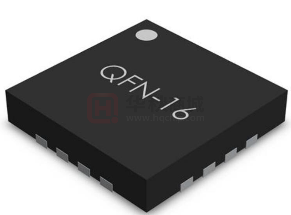
Small 2.5mmx3.2mm QFN-16 Package
Wide 2.7V to 7V Operating Input Range
Programmable Storage Voltage up to 30V
Up to 4.6A Programmable Input Current
Limit
Up to 3A Buck Release Current Capability
Reverse Current Block of Input Switch
6V Bus Clamping Voltage
Adjustable DVDT Slew Rate for VB Start-Up
Bus Power Good Indicator
1.2MHz Buck Release Mode Switching
Frequency
Internal 60mΩ Hot-Swap Switch
Internal 100mΩ and 80mΩ Power Switches
for Energy Storage and Release
Management Circuits
Thermal Protection
APPLICATIONS
The MP5507E requires a minimal number of
readily
available,
standard,
external
components and is available in a QFN-16
(2.5mmx3.2mm) package.
Solid-State Drives
Hard-Disk Drives
Power Back-Up Systems
All MPS parts are lead-free, halogen-free, and adhere to the RoHS directive.
For MPS green status, please visit the MPS website under Quality
Assurance. “MPS” and “The Future of Analog IC Technology” are registered
trademarks of Monolithic Power Systems, Inc.
TYPICAL APPLICATION
VB to DCDC
R1
10.7k
C2
22μF
R2
4.02k
C1
0.1μF
D1
TVS
optional
for spike
VB
C4
100nF
BST
FBB
SW
VBO
VIN
STRG
ENCH
DISC
MP5507E
FBS
ILIM
R5
1.2k
DVDT
PGB
PGND
CST
L1
1μH
R3
200k
R4
14k
C3
AGND
MP5507E Rev. 1.0
www.MonolithicPower.com
6/29/2016
MPS Proprietary Information. Patent Protected. Unauthorized Photocopy and Duplication Prohibited.
© 2016 MPS. All Rights Reserved.
1
�MP5507E – 7V, 3A, ENERGY STORAGE AND MANAGEMENT UNIT
ORDERING INFORMATION
Part Number*
MP5507EGRG
Package
QFN-16 (2.5mmx3.2mm)
Top Marking
See Below
* For Tape & Reel, add suffix –Z (e.g. MP5507EGRG–Z)
TOP MARKING
AVU: Product code of MP5507E
Y: Year code
WW: Week code
LLL: Lot number
PACKAGE REFERENCE
TOP VIEW
VIN
16
VB
VBO
15
14
DVDT
1
13
FBS
ILIM
2
12
FBB
PGB
3
11
AGND
DISC
4
10
CST
ENCH
5
9
BST
6
7
8
PGND
SW
STRG
QFN-16 (2.5mmx3.2mm)
MP5507E Rev. 1.0
www.MonolithicPower.com
6/29/2016
MPS Proprietary Information. Patent Protected. Unauthorized Photocopy and Duplication Prohibited.
© 2016 MPS. All Rights Reserved.
2
�MP5507E – 7V, 3A, ENERGY STORAGE AND MANAGEMENT UNIT
ABSOLUTE MAXIMUM RATINGS (1)
Thermal Resistance
Supply voltage (VIN) ....................................8.0V
VSTRG .............................................. -0.3V to 35V
VSW ................................... -0.3V to VSTRG + 0.3V
VBST .................................. -0.3V to VSTRG + 6.5V
VCST ............................................... -0.3V to 40V
All other pins ................................. -0.3V to 6.5V
(2)
Continuous power dissipation (TA = +25°C)
................................................................ 2.08W
Junction temperature ............................... 150°C
Lead temperature .................................... 260°C
Operating temperature ............... -40°C to +85°C
QFN-16 (2.5mmx3.2mm) ....... 60 ...... 14 ... °C/W
Recommended Operating Conditions
(3)
(4)
θJA
θJC
NOTES:
1) Exceeding these ratings may damage the device.
2) The maximum power dissipation is a function of the maximum
junction temperature TJ (MAX), the junction-to-ambient
thermal resistance θJA, and the ambient temperature TA. The
maximum continuous power dissipation at any ambient
temperature is calculated by PD (MAX) = (TJ (MAX)-TA)/θJA.
Exceeding the maximum allowable power dissipation
produces an excessive die temperature, causing the regulator
to go into thermal shutdown. Internal thermal shutdown
circuitry protects the device from permanent damage.
3) The device is not guaranteed to function outside of its
operating conditions.
4) Measured on JESD51-7, 4-layer PCB.
Supply voltage (VIN) .......................... 2.7V to 7V
Bus voltage (VB)................................ 2.7V to 6V
Storage voltage (VSTRG)...................... VIN to 30V
Max. input current .......................................4.6A
Max. buck release current .............................3A
Operating junction temp. (TJ). .. -40°C to +125°C
MP5507E Rev. 1.0
www.MonolithicPower.com
6/29/2016
MPS Proprietary Information. Patent Protected. Unauthorized Photocopy and Duplication Prohibited.
© 2016 MPS. All Rights Reserved.
3
�MP5507E – 7V, 3A, ENERGY STORAGE AND MANAGEMENT UNIT
ELECTRICAL CHARACTERISTICS
VIN = 5.0V, TA = 25°C, unless otherwise noted.
Parameter
Input supply voltage range
Supply current (quiescent)
VIN under-voltage lockout
threshold rising
VIN under-voltage lockout
threshold hysteresis
ENCH high threshold rising
ENCH low threshold falling
DISC high threshold rising
DISC low threshold
falling
VIN to VB current limit FET on
resistance
Symbol
VIN
IQ
0.3
0.4
DISCF
0.4
RDS(ON)
7
2
V
mA
2.5
2.7
V
0.4
0.5
V
1.2
V
1.2
V
V
VCLAMP
V
mΩ
60
RILIM = 1.4kΩ
VIN = 6V, VB = 0V or
VB = 6V, VIN = 0V
VIN = 7V
DVDT floating
Rise time (DVDT)
τR
Connect a capacitor to DVDT,
test DVDT charge current
Internal reset delay time
τD
Power on to VB rise delay
PGB low threshold
PGB delay
PGB sink current capability
PGB leakage current
Buck-mode dumping peak
current limit
Release-buck switching
frequency
Units
VENCH = 2V, VFBB/FBS = 1V
ENCHF
DISCR
ILEAK
Boost disconnect switch Ron
Energy management HS Ron
Energy management LS Ron
Feedback voltage
Feedback current
PGB high threshold
Max
ENCHR
Off-state leakage current
Charge peak current in boost
mode
Typ
2.7
INUVHYS
ILIM
Pre-charge current
Min
INUVR
Continuous current limit
VB clamping voltage
Condition
3.24
5.5
3.6
6
0.8
3.96
A
2
μA
6.5
V
ms
2
μA
1.1
ms
ICH-PRE
130
mA
ICH
500
mA
25
100
80
0.79
mΩ
mΩ
mΩ
V
nA
VFBB
Rdison
RHon
RLon
VFBB, VFBS
IFBB
VFBB = VFBS = 0.79V
PGH_B
PGL_B
PGD_B
Falling
Sink 4mA
VPGB = 3.3V
0.782
0.81
50
1.03
1
0.5
0.3
120
VFBB
μs
V
nA
IDUMP
5
A
fs_RLS
1.2
MHz
MP5507E Rev. 1.0
www.MonolithicPower.com
6/29/2016
MPS Proprietary Information. Patent Protected. Unauthorized Photocopy and Duplication Prohibited.
© 2016 MPS. All Rights Reserved.
4
�MP5507E – 7V, 3A, ENERGY STORAGE AND MANAGEMENT UNIT
ELECTRICAL CHARACTERISTICS (continued)
VIN = 5.0V, TA = 25°C, unless otherwise noted.
Parameter
VB under-voltage lockout
(5)
threshold rising
VB under-voltage lockout
(5)
threshold hysteresis
(6)
Thermal shutdown
(6)
Thermal shutdown hysteresis
Symbol
Condition
Min
Typ
Max
Units
INUVBR
1.8
2.2
2.5
V
INUVBHYS
0.15
0.25
0.35
V
TSD
THYS
150
30
°C
°C
NOTES:
5) VB UVLO is applied to energy storage and release circuitry.
6) Guaranteed by characterization, not tested in production.
MP5507E Rev. 1.0
www.MonolithicPower.com
6/29/2016
MPS Proprietary Information. Patent Protected. Unauthorized Photocopy and Duplication Prohibited.
© 2016 MPS. All Rights Reserved.
5
�MP5507E – 7V, 3A, ENERGY STORAGE AND MANAGEMENT UNIT
TYPICAL PERFORMANCE CHARACTERISTICS
VIN = 3.3V, VSTRG = 12V, VRLS = 2.9V, L = 1µH, TA = 25°C, unless otherwise noted.
MP5507E Rev. 1.0
www.MonolithicPower.com
6/29/2016
MPS Proprietary Information. Patent Protected. Unauthorized Photocopy and Duplication Prohibited.
© 2016 MPS. All Rights Reserved.
6
�MP5507E – 7V, 3A, ENERGY STORAGE AND MANAGEMENT UNIT
TYPICAL PERFORMANCE CHARACTERISTICS (continued)
Performance waveforms are tested on the evaluation board of the Design Example section.
VIN = 3.3V, VSTRG = 12V, VRLS = 2.9V, L = 1µH, TA = 25°C, unless otherwise noted.
MP5507E Rev. 1.0
www.MonolithicPower.com
6/29/2016
MPS Proprietary Information. Patent Protected. Unauthorized Photocopy and Duplication Prohibited.
© 2016 MPS. All Rights Reserved.
7
�MP5507E – 7V, 3A, ENERGY STORAGE AND MANAGEMENT UNIT
TYPICAL PERFORMANCE CHARACTERISTICS (continued)
Performance waveforms are tested on the evaluation board of the Design Example section.
VIN = 3.3V, VSTRG = 12V, VRLS = 2.9V, L = 1µH, TA = 25°C, unless otherwise noted.
MP5507E Rev. 1.0
www.MonolithicPower.com
6/29/2016
MPS Proprietary Information. Patent Protected. Unauthorized Photocopy and Duplication Prohibited.
© 2016 MPS. All Rights Reserved.
8
�MP5507E – 7V, 3A, ENERGY STORAGE AND MANAGEMENT UNIT
PIN FUNCTIONS
QFN-16 Pin #
Name
1
DVDT
2
ILIM
3
PGB
4
DISC
5
ENCH
6
PGND
7
SW
8
STRG
9
BST
10
CST
11
12
13
AGND
FBB
FBS
14
VBO
15
VB
16
VIN
Description
VB voltage slew-rate control. Connect a capacitor from DVDT to AGND to
program the VB charge-up slew rate. Leave DVDT floating for the default soft-start
time (around 0.8ms from 0V to 5V).
Input current limit setting. Connect a resistor between ILIM and AGND to adjust
the DC limit from VIN to VB. ILIM cannot be left floating. Pull ILIM higher than 1V to
turn off the VIN-to-VB MOSFET. Do not pull ILIM up to a voltage source higher than
the maximum of VIN and VB.
VB power good indicator. PGB is an open-drain output. PGB goes high if the FBB
voltage exceeds 1.03xVFBB (typically 0.813V). PGB goes low if the FBB voltage
drops below 1.0xVFBB (0.79V).
On/off control for the VIN-to-VB isolation FET. When DISC is pulled down, the
VIN-to-VB isolation FET is turned off. When DISC is pulled high, the VIN-to-VB
isolation FET is turned on. It is recommended to pull DISC up to VIN through a 100k
resistor for automatic start-up.
On/off control for the charge/release circuitry. When ENCH is pulled down, the
charge/release circuitry is disabled. ENCH must be kept high to achieve energy
release.
Power ground.
Switch output for the charge/release circuitry. Connect a small inductor between
SW and VBO.
Storage voltage. Connect the appropriate storage capacitors for energy storage
and release operation.
Bootstrap for the charge/release circuitry. The internal bidirectional switcher
requires a bootstrap capacitor (typically 100nF) from BST to SW to supply high-side
switch-driver voltage during release.
High-side switch driving voltage storage. CST is charged by the storage power
when the storage voltage is high and supports driver voltage when the storage
voltage drops close to the VB regulated voltage.
IC signal ground.
Bus voltage feedback sense. FBB sets the bus release voltage.
Storage voltage feedback sense. FBS sets the storage voltage.
Source of internal isolation FET. Connect the inductor between SW and VBO for
boost and buck operation.
Bus voltage. A 22μF to 47μF ceramic capacitor is required as close to VB as
possible.
Input supply voltage. The MP5507E operates from an unregulated 2.7V to 7V
input. Place a ceramic capacitor 0.1µF or larger as close to VIN as possible. A TVS
diode at the input is necessary if the VIN voltage spike is high. Refer to the
Selecting the Input Capacitor and TVS section on page 14 for additional details.
MP5507E Rev. 1.0
www.MonolithicPower.com
6/29/2016
MPS Proprietary Information. Patent Protected. Unauthorized Photocopy and Duplication Prohibited.
© 2016 MPS. All Rights Reserved.
9
�MP5507E – 7V, 3A, ENERGY STORAGE AND MANAGEMENT UNIT
BLOCK DIAGRAM
To DC/DC Converter
FBB
VB
VBO
SW
BST
CST
STRG
VIN
HS Driver
FBS
Charge Pump
Current Limit and Energy
Backup Management Circuit
LS Driver
PGND
DVDT DISC ILIM ENCH PGB AGND
Figure 1: Functional Block Diagram
MP5507E Rev. 1.0
www.MonolithicPower.com
6/29/2016
MPS Proprietary Information. Patent Protected. Unauthorized Photocopy and Duplication Prohibited.
© 2016 MPS. All Rights Reserved.
10
�MP5507E – 7V, 3A, ENERGY STORAGE AND MANAGEMENT UNIT
OPERATION
The MP5507E is an energy storage and
management unit in a QFN-16 (2.5mmx3.2mm)
package. The MP5507E provides a very
compact and efficient power backup solution for
typical solid-state drive applications. MPS’
patented lossless energy storage and release
management circuits use a bidirectional
buck/boost converter to achieve optimal energy
transfer and provide a cost-effective energy
storage solution.
The MP5507E’s built-in boost converter
charges the bulk storage capacitors to a
programmed voltage when the system is
powered up. If an input power outage occurs,
the MP5507E indicates a VB bus power failure,
disconnects the input switch, and transfers the
energy from the storage capacitor to VB
through the built-in buck converter, holding the
bus voltage to a regulated voltage when the
system consumes energy for data backup. The
buck converter can work in 100% duty cycle
operation to deplete the stored energy
completely. Depending on different power
backup times and storage components from
different applications, the MP5507E can provide
a compact solution with a programmable
storage voltage setting.
Start-Up
When VIN starts up, the VB bus voltage is
charged from 0 to VIN. The VB rising slew rate
is controlled by the DVDT capacitance. This
function prevents input inrush current and
provides protection to the downstream system.
EHCH is used to enable and disable the
storage charge and release circuitry. The
storage charge circuitry operate in two modes:
pre-charge mode (the STRG voltage is charged
to the VB voltage from 0V using a current
source) and boost mode (the STRG voltage is
charged to set the voltage). The pre-charge
mode charges the STRG voltage up to the VB
voltage using a near-constant current source
(around 130mA). When the STRG voltage is
close to VB, and the VB voltage is higher than a
certain threshold (where PGB rises high), boost
mode is initiated.
If ENCH is already high before VIN rises to the
UVLO threshold, the storage charge circuitry
starts a linear charge automatically when VIN is
higher than the UVLO threshold (typically 2.5V),
switches to boost switching mode when the
storage voltage is charged close to VB, and
PGB rises high. If ENCH rises high after VB,
DVDT elapses and PGB has raised high, precharge begins, followed by boost switching.
Boost mode charges the STRG voltage to the
target voltage. The charging build-up process
when ENCH is high before VB starts up is
shown in Figure 2.
It is strongly recommended to enable ENCH
after VB has settled (see Figure 3). Because
the release mode is triggered when the FBB
voltage is lower than 0.79V (although there is a
23mV hysteresis between boost mode and
release mode), the VB voltage may be pulled
back low and accidently enter release mode. To
prevent this, enable ENCH after VB settles if
the system I/O can be used to control ENCH.
The charging build-up process when ENCH is
enabled after VB settles is shown in Figure 3.
VIN
UVLO
ENCH
VB DVDT
Charge Up
FBB=0.813V
VB
STRG Boost Mode
VSTRG
STRG Pre-charge Mode
Power-on Delay Time
Figure 2: Charging Process
VIN
UVLO
ENCH
VB
VB DVDT
Charge Up
STRG Boost Mode
VSTRG
STRG Pre-charge Mode
Power-on Delay Time
Figure 3: Charging Process when ENCH is
Enabled after VB Settles
MP5507E Rev. 1.0
www.MonolithicPower.com
6/29/2016
MPS Proprietary Information. Patent Protected. Unauthorized Photocopy and Duplication Prohibited.
© 2016 MPS. All Rights Reserved.
11
�MP5507E – 7V, 3A, ENERGY STORAGE AND MANAGEMENT UNIT
Storage Voltage
After the storage voltage charges up, the internal
boost converter regulates it to the regulated
voltage automatically. The MP5507E uses burst
mode to minimize the converter’s power loss.
When the storage voltage drops below the set
voltage, burst mode is initiated and charges the
storage capacitor. During the burst period, the
current limit and the low-side MOSFET (LS-FET)
control the switching. When the LS-FET turns on,
then the inductor current increases until it
reaches the current limit (about 500mA). After
reaching the current limit, the LS-FET turns off
for the set minimum off time. At the end of this
minimum off time, if the feedback voltage
remains below the 0.79V internal reference, the
LS-FET turns on again. Otherwise, the
MP5507E waits until the voltage drops below the
threshold before turning on the LS-FET. During
boost mode, the HS-FET is turned off, and the
body diode of the HS-FET conducts the current.
Release
The MP5507E monitors the input voltage and
bus voltage continuously. Once the bus voltage
drops below the release voltage (mostly due to
the input voltage outage), the internal boost
converter stops charging and works in buckrelease mode. In buck mode, the part transfers
energy from the high-voltage storage capacitor
to the low-voltage bus capacitor. Determine the
release voltage by selecting resistor values for
the bus resistor divider.
VSTRG
VB
VB Release
Regulated Voltage
PGB
Figure 4: Release Times
The released buck applies the fixed-frequency
constant-on-time (COT) control and enables a
fast transition between the charge and release
modes. The buck converter works at 100% duty
cycle until the storage capacitor voltage
approaches the bus voltage. Then the storage
and VB voltages drop until they reach the
DC/DC converter’s UVLO threshold (see Figure
4).
Input Current Limit Switch
The input current limit switch controls the input
inrush current of the internal hot-swap MOSFET
to prevent an inrush current from the input to
the VB capacitor. A capacitor connected to
DVDT sets the VB rising soft-start time. Despite
the soft-start process, ILIM can limit the steadystate current. Connect a resistor between ILIM
and GND to set the current limit.
Reverse-Current Protection
The hot-swap circuit uses reverse-current
protection to prevent the storage energy from
transferring back to the input when energy is
released from the storage capacitors to the bus.
The hot-swap MOSFET turns on when the input
voltage exceeds the VIN UVLO threshold
during start-up or when the input voltage is
about 0.2V higher than the VB voltage during
VIN power recovery. The hot-swap MOSFET
turns off when the input voltage falls below the
VB voltage during release or when PGB drops.
DVDT
Connect a capacitor across DVDT to program
the soft-start time. Depending on the system
inrush current requirement, different DVDT
capacitors can be selected to program the
inrush current during system start-up.
VIN-to-VB Switch Off Control (DISC)
When DISC is pulled low, the VIN-to-VB
MOSFET switches off directly. If ENCH is high,
the MP5507E enters buck mode once VB drops
to the VB regulation threshold (see Figure 5).
The VIN-to-VB switch cannot turn on until DISC
is high. Pull DISC up to VIN through a 100k
resistor for automatic start-up.
MP5507E Rev. 1.0
www.MonolithicPower.com
6/29/2016
MPS Proprietary Information. Patent Protected. Unauthorized Photocopy and Duplication Prohibited.
© 2016 MPS. All Rights Reserved.
12
�MP5507E – 7V, 3A, ENERGY STORAGE AND MANAGEMENT UNIT
VSTRG
VB
VB Release
Regulated Voltage
PGB
DISC
Thermal Shutdown
Thermal shutdown is implemented to prevent the
chip from thermal damage. When the silicon die
temperature is higher than its upper threshold,
the entire chip shuts down. When the
temperature is below its lower threshold, the
chip turns on again if VIN power is available.
However, if thermal shutdown occurs in buck
mode without VIN power, the chip will not turn
on again, even if STRG has a power supply.
Figure 5: DISC Off
Bus Power-Good Indicator (PGB)
When the voltage on FBB (bus feedback) falls
below 1.0xVFBB, the MP5507E pulls PGB low to
indicate the release status. When the FBB
voltage rises above 1.03xVFBB, the MP5507E
pulls PGB high to indicate the input power good
status.
MP5507E Rev. 1.0
www.MonolithicPower.com
6/29/2016
MPS Proprietary Information. Patent Protected. Unauthorized Photocopy and Duplication Prohibited.
© 2016 MPS. All Rights Reserved.
13
�MP5507E – 7V, 3A, ENERGY STORAGE AND MANAGEMENT UNIT
APPLICATION INFORMATION
Selecting the Input Capacitor and TVS
Capacitors at VIN are recommended to absorb
possible voltage spikes during input power turnon, input switch hard-off (during power-off), or
other special conditions. The application
determines the capacitor. For example, if the
input power trace is too long (with a higher
parasitic inductance) during the input switch
hard-off period, more energy is pumped into the
input. This means that more input capacitors are
needed to ensure that the input voltage spike
remains in a safe range. Use a capacitor 0.1µF
or larger based on the spike condition.
Consider inrush current requirements when
selecting an input capacitor. Typically, more
input capacitors result in a higher input inrush
current during hot-plugging. A smaller input
capacitor is needed for a smaller inrush current.
The MP5507E works normally with a very small
input capacitor. However, this leads to a possible
high-voltage spike. An efficient solution is to add
a TVS diode at the input to absorb the possible
input-voltage spike. Simultaneously, keep the
inrush current small during hot-plugging. A TVS
diode such as the SMA6J5.0A is recommended.
R3 and R4 are not critical for normal operation.
Select R3 and R4 to be higher than 10kΩ to
account for the bleed current. For example, if R4
is 14kΩ, then R3 can be calculated with
Equation (2):
R3
14k ( VSTORAGE VFBS )
VFBS
(2)
For a 12V storage voltage, R3 is 200kΩ.
Table 1 lists the recommended resistors for
different storage voltages.
Table 1: Resistor Pairs for VSTORAGE
VSTORAGE (V)
8
12
20
R3 (kΩ)
127
200
340
R4 (kΩ)
14
14
14
Selecting the Release Voltage and VBUS
Capacitors
Select the release voltage by choosing the
external feedback resistors R1 and R2 (see
Figure 7).
Setting the Storage Voltage
Set the storage voltage by choosing the external
feedback resistors R3 and R4 (see Figure 6).
Figure 7: Release Feedback Circuit
The release voltage (VRELEASE) can be calculated
with Equation (3):
R3
FBS
Cstorage
VRELEASE (1
R4
Figure 6: Storage Feedback Circuit
The storage voltage can be determined with
Equation (1):
VSTORAGE (1
R3
) VFBS
R4
Where VFBS is 0.79V, typically.
(1)
R1
) VFBB
R2
(3)
VFBB is 0.79V, typically. However, R1 and R2 not
only determine the release voltage, but also
affect loop stability. Choose R2 a with 2k to 10k
resistor (4.02k is typically recommended) for the
low-side divider resistor for stable performance
with CB = 22μF. Table 2 lists the recommended
resistor values for different release voltages.
Table 2: Resistor Pairs for VRELEASE
VRELEASE (V)
4.2
2.9
R1 (kΩ)
17.4
10.7
MP5507E Rev. 1.0
www.MonolithicPower.com
6/29/2016
MPS Proprietary Information. Patent Protected. Unauthorized Photocopy and Duplication Prohibited.
© 2016 MPS. All Rights Reserved.
R2 (kΩ)
4.02
4.02
14
�MP5507E – 7V, 3A, ENERGY STORAGE AND MANAGEMENT UNIT
Selecting the Storage Capacitor
The storage capacitor stores energy during
normal operation and releases it to VB when VIN
loses input power. Use a general-purpose
electrolytic capacitor or low-profile POS
capacitor for most applications. One 4.7µF
ceramic capacitor in parallel with the storage
capacitor is recommended if the electrolytic
capacitor ESR is high.
Select a storage capacitor with a voltage rating
that exceeds the targeted storage voltage.
Consider the capacitance reduction with the DC
voltage offset when choosing the capacitor.
Different capacitors have a different capacitance
de-rating performance. Choose a capacitor with
enough of a voltage rating to guarantee
sufficient capacitance.
The required capacitance depends on the time
of the dying gasp for a typical application.
Assume the release current is IRELEASE when the
VB voltage is regulated at VRELEASE for the
DC/DC converter, the storage is VSTORAGE, and
the required dying gasp time is τDASP. The
required storage capacitance can then be
calculated with Equation (4):
CS
2 VRELEASE IRELEASE DASP
2
2
VSTORAGE
VRELEASE
(4)
Consider the power loss during release. The
buck converter efficiency is about 85% in most
applications. Select storage capacitance at
1.18xCS to ensure enough releasing time. If
IRELEASE = 1A, τDASP = 20ms, VSTORAGE = 12V, and
VRELEASE = 4.2V, then the required storage
capacitance is 1570μF.
For typical applications using a 5V input supply,
set the storage voltage above 10V to fully utilize
the high-voltage energy and minimize the
storage capacitance requirements. Generally,
16V POS capacitors or 25V electrolytic
capacitors are recommended.
Selecting the External Diode
An external diode parallel with the high-side
power MOSFET (HS-FET) is optional for normal
charge-mode operation. This diode improves the
boost efficiency slightly. The diode voltage rating
should be higher than the storage voltage, and
the current rating should be higher than the
boost charge current.
Setting the Input Hot-Swap Current Limit
Connect a resistor from ILIM to GND to set the
current-limit value. For example, a 1.2kΩ resistor
sets the current limit to about 4.1A. Table 3 lists
the recommended resistors for different current
limit values.
Table 3: ILIM vs. RLIM
ILIM (A)
4.6
4.1
3.6
1.6
RLIM (kΩ)
1.07
1.2
1.4
3.2
Selecting the Inductor
The inductor is necessary to supply constant
current to the load. Since boost mode and buck
mode share the same inductor, and generally
the buck mode current is higher, an inductor that
at least supports the buck mode releasing
current is recommended.
Select the inductor based on the buck-release
mode. If the storage voltage is VS, then the
release voltage is VR, and the buck running is
fixed at a 1.2MHz frequency. The inductance
value can be calculated with Equation (5):
L
VR
V
(1 R )
IL FSW
VS
(5)
Where ∆IL is the peak-to-peak inductor ripple
current.
The inductor should not saturate under the
maximum inductor peak current.
Setting the Bus Voltage Rise Time
Connect a capacitor to DVDT to set the bus
voltage start-up slew rate and soft-start time.
Leave DVDT floating for the default soft-start
time (around 0.8ms from 0V to 5V). Table 4 lists
the recommended capacitors for different softstart times at a 5V input condition.
Table 4: Soft-Start vs. Capacitor Value
τR (ms)
5.3
53
Cdv/dt (nF)
10
100
MP5507E Rev. 1.0
www.MonolithicPower.com
6/29/2016
MPS Proprietary Information. Patent Protected. Unauthorized Photocopy and Duplication Prohibited.
© 2016 MPS. All Rights Reserved.
15
�MP5507E – 7V, 3A, ENERGY STORAGE AND MANAGEMENT UNIT
PCB Layout Guidelines
Efficient PCB layout is critical for stable
operation. A 4-layer layout is recommended to
achieve better thermal performance and simplify
layout. For best results, refer to Figure 8 and
Figure 9 and follow the guidelines below.
1) Use short, wide, and direct traces in the highcurrent paths (VIN, VB, VBO, SW, STRG, and
PGND).
2) Place the decoupling capacitor as close to VB
and PGND as possible.
3) Place the decoupling capacitor as close to
STRG and PGND as possible.
4) Keep the switching node SW short and away
from the feedback network.
5) Place the external feedback resistors as close
to FB as possible.
6) Keep the BST voltage path (BST, C4, and
SW) as short as possible.
Inner 1 Layer
VB to DCDC
R1
C2
R2
SW
VBO
VIN
C1
D1
C4
BST
VB
FBB
TVS
optional
for spike
L1
STRG
ENCH
DISC
DVDT
R5
MP5507E
R3
FBS
ILIM
R4
C3A
C3B
PGB
PGND
AGND
CST
Inner 2 Layer
Figure 8: Schematic for Layout
PGND
PGND
1
2
C3B
STRG
SW
PGND
1
2
SW
VBO
C3A
C4
2
U1
SW
STRG
PGND
BST
DISC
1
ILIM
FBS
DVDT
VIN
VB
2
VB
FBB
VBO
R1
PGB
PGND
2
R5
AGND
C1
R4
1
2
R3
2
1
1
R5
1
2
1
VB
1
1
C2
2
2
PGND
Top Layer
PGND
D1
PGND
R2
PGND
ENCH
CST
AGND
VB
AGND
2
VIN
1
Bottom Layer
Figure 9: Recommended Layout
MP5507E Rev. 1.0
www.MonolithicPower.com
6/29/2016
MPS Proprietary Information. Patent Protected. Unauthorized Photocopy and Duplication Prohibited.
© 2016 MPS. All Rights Reserved.
16
�MP5507E – 7V, 3A, ENERGY STORAGE AND MANAGEMENT UNIT
Design Example
Table 5 is a design example following the
application guidelines for the specifications below.
The detailed application schematic is shown in
Figure 10. The typical performance and circuit
waveforms are shown in the Typical Performance
Characteristics section. For more device
applications, please refer to the related
evaluation board datasheet.
Table 5: Design Example
Parameter
Input voltage
Storage voltage
Bus backup
voltage
Bus backup
max load
Symbol
VIN
VSTRG
Value
3.3
12
Units
V
V
VRLS
2.9
V
IRELEASE
3
A
VB
C2A
R1
AGND
R2
C2B
R8
22µF
10K
VB
10.7K
1µF
FBB
PGB
VIN
CST
PGND
4.02K
VIN
AGND
C1
D1
PGND
1µF
0.1µF
PGND
SMA6J5.0A
C6
R7
R6
PGND
100K
100K
MP5507E
ENCH
BST
C4
100nF
SW
L1
DISC
VBO
ILIM
C5
10nF
AGND
R3
AGND
AGND
STRG
STRG
PGND
R5
1.2k
1µH
DVDT
200K
FBS
R4
C3A
4.7µF
PGND
C3B
100µF
PGND
C3C
100µF
PGND
14K
PGND
AGND
AGND
Figure 10: Detailed Application Schematic
MP5507E Rev. 1.0
www.MonolithicPower.com
6/29/2016
MPS Proprietary Information. Patent Protected. Unauthorized Photocopy and Duplication Prohibited.
© 2016 MPS. All Rights Reserved.
17
�MP5507E – 7V, 3A, ENERGY STORAGE AND MANAGEMENT UNIT
PACKAGE INFORMATION
QFN-16 (2.5mmx3.2mm)
PIN 1 ID
PIN 1 ID
MARKING
PIN 1 ID
INDEX AREA
TOP VIEW
BOTTOM VIEW
SIDE VIEW
0.10x45°
NOTE:
1) ALL DIMENSIONS ARE IN MILLIMETERS.
2) LEAD COPLANARITY SHALL BE 0.10
MILLIMETERS MAX.
3) JEDEC REFERENCE IS MO-220.
4) DRAWING IS NOT TO SCALE.
RECOMMENDED LAND PATTERN
NOTICE: The information in this document is subject to change without notice. Please contact MPS for current specifications.
Users should warrant and guarantee that third party Intellectual Property rights are not infringed upon when integrating MPS
products into any application. MPS will not assume any legal responsibility for any said applications.
MP5507E Rev. 1.0
www.MonolithicPower.com
6/29/2016
MPS Proprietary Information. Patent Protected. Unauthorized Photocopy and Duplication Prohibited.
© 2016 MPS. All Rights Reserved.
18
�Mouser Electronics
Authorized Distributor
Click to View Pricing, Inventory, Delivery & Lifecycle Information:
Monolithic Power Systems (MPS):
MP5507EGRG-Z MP5507EGRG-P
�