MP62550/MP62551
Precision 60mA-1.7A Programmable
Current-Limited Power Distribution Switch
The Future of Analog IC Technology
DESCRIPTION
FEATURES
MP62550/MP62551 Power Distribution Switch
is designed for precision current limiting and
provides up to 1.5A continuous output current.
It offers programmable current limit between
60mA and 1.7A (typ) with ±10% accuracy by an
external resistor. The switch includes an 88mΩ
N-channel Power MOSFET and operates from
2.5V to 5.5V input voltage.
The device has built-in protection for both over
current and increased thermal stress. For over
current, the device will limit the current by
changing to a constant current mode. It will
shutdown when its internal temperature
reaches unsafe levels and recover once the
device temperature reduces approx 10C.
It provides built-in soft-start which controls the
rise and fall times of the output voltage to limit
the initial inrush current and voltage surges.
The reverse-voltage protection feature turns off
the MOSFET to protect the device.
Up to 1.5A Continuous Output Current
±10% Current-Limit Accuracy
Adjustable Current-Limit, 60mA -1700mA (typ)
Fast Over-current Response 2μs (typ)
2.5V to 5.5V Supply Range
88mΩ MOSFET (TQFN Package)
1.5μA Maximum Standby Supply Current
Reverse Input-Output Voltage Protection
Built-in Soft-Start
Thermal-Shutdown Protection
Automatic-on after Fault Removed
Under-Voltage Lockout
Deglitched Fault Report
FLAG won't Change State at Input UVLO
Transition
Bidirectional Fault Deglitch Time
Active Low & Active High Options
________
APPLICATIONS
________
The FLAG output will report a fail mode (low
level) when over current or over temperature is
________
encountered. The FLAG will not change state
when the input UVLO is triggered.
The MP62550/MP62551 is available in space
saving 6-pin TQFN 2x2mm package and
TSOT23-6 package.
Smart Phone and PDA
Portable GPS Device
Notebook PC
Set-top-box
Telecom and Network Systems
PC Card Hot Swap
USB Power Distribution
All MPS parts are lead-free, halogen free, and adhere to the RoHS directive.
For MPS green status, please visit MPS website under Quality
Assurance. “MPS” and “The Future of Analog IC Technology” are Registered
Trademarks of Monolithic Power Systems, Inc.
TYPICAL APPLICATION
GND
VIN
FLAG
R FLAG
10k
OUT
IN
FLAG
ILIM
EN *
GND
+
VOUT
R ILIM
EN*
GND
PAD
MP62551
(*EN active low for MP62550)
MP62550/MP62551 Rev. 1.3
www.MonolithicPower.com
4/1/2019
MPS Proprietary Information. Patent Protected. Unauthorized Photocopy and Duplication Prohibited.
© 2019 MPS. All Rights Reserved.
1
�MP62550/MP62551 –60mA-1.7A PROGRAMMABLE CURRENT-LIMITED POWER DISTRIBUTION SWITCHES
ORDERING INFORMATION
Part Number*
Enable
MP62550DGT
Active Low
MP62551DGT Active High
MP62550DJ
Active Low
MP62551DJ
Active High
Maximum
Switch Continuous Load
Current
Single
1.5A
Single
1.5A
Package
Top Marking
Free Air
Temperature (TA)
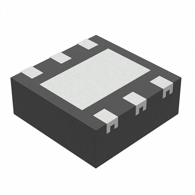
TQFN6 (2x2mm)
TQFN6 (2x2mm)
5Y
AJ
-40C to +85C
TSOT23-6
5Y
TSOT23-6
AAN
-40C to +85C
* For Tape & Reel, add suffix –Z (e.g. MP62551DGT–Z).
For RoHS compliant packaging, add suffix –LF (e.g. MP62551DGT–LF–Z)
PACKAGE REFERENCE
TOP VIEW
TOP VIEW
OUT
1
6
IN
ILIM
2
5
GND
FLAG
3
4
EN
EXPOSED
PAD ON
BACKSIDE
IN
1
6
OUT
GND
2
5
ILIM
EN
3
4
FLAG
TSOT23-6
TQFN6 (2x2mm)
MP62550/MP62551
Single-Channel
(EN active low for MP62550)
ABSOLUTE MAXIMUM RATINGS (1)
IN to GND..................................... -0.3V to +6.5V
________
ILIM, EN, FLAG, OUT to GND..... -0.3V to +6.5V
RILIM Range (1%) ...................... 12.4kΩ to 210kΩ
Continuous Power Dissipation (TA = +25°C) (2)
TQFN(2x2)-6 ............................................. 1.56W
TSOT23-6 ................................................. 0.57W
Lead Temperature .................................... 260°C
Storage Temperature ................-65°C to +150°C
Maximum Junction Temp. (TJ) .............. +125°C
Thermal Resistance (3)
θJA
θJC
TQFN6 (2x2mm)…. ................. 80 ...... 16... C/W
TSOT23-6…. .......................... 220 .... 110.. C/W
Notes:
1) Exceeding these ratings may damage the device.
2) The maximum allowable power dissipation is a function
of the
maximum junction temperature TJ(MAX), the junctiontoambient thermal resistance θJA, and the ambient
temperature TA. The maximum allowable continuous power
dissipation at any ambient temperature is calculated by
PD(MAX)=(TJ(MAX)-TA)/θJA.
Exceeding
the
maximum
allowable power dissipation will cause excessive die
temperature, and the regulator will go into thermal shutdown.
Internal thermal shutdown circuitry protects the device from
permanent damage.
3) Measured on JESD51-7, 4-layer PCB.
MP62550/MP62551 Rev. 1.3
www.MonolithicPower.com
4/1/2019
MPS Proprietary Information. Patent Protected. Unauthorized Photocopy and Duplication Prohibited.
© 2019 MPS. All Rights Reserved.
2
�MP62550/MP62551 –60mA-1.7A PROGRAMMABLE CURRENT-LIMITED POWER DISTRIBUTION SWITCHES
ELECTRICAL CHARACTERISTICS
TA=+25°C, 2.5V≤VIN≤5.5V, 12.4kΩ≤RILIM≤210kΩ, RFLAG=10kΩ, unless otherwise noted.
Parameters
IN Voltage Range
Symbol
VIN
Test Conditions
Min
2.5
Typ
Max
5.5
TQFN2x2-6
88
135
TSOT23-6
100
135
125
145
μA
1.5
μA
0.01
1
μA
1530
1700
1870
960
1190
1360
450
510
570
105
135
166
45
60
85
FET On_Resistance
RDS(on)
VIN=5V,
IOUT=100mA
-40°C≤TA≤+85°C
Supply Current
IIN_ON
Device Enabled, VOUT=float, VIN=5.5V
Shutdown Current
IIN_OFF
Device Disabled, VOUT=float, VIN=5.5V
Reverse
Current
Leakage
IREV
VIN=0V, VOUT=5.5V
RILIM=13kΩ
RILIM=20kΩ
Current Limit
(See Figure 2)
IOS
RILIM=49.9kΩ
RILIM=210kΩ
-40°C≤TA≤85°C,
OUT connected
to GND
ILIM Shorted to IN
Short Current Response
Time
TIOS
Under-voltage Lockout
INUVVTH
Under-voltage Hysteresis
INUVHYS
EN Input Logic High
Voltage
EN Input Logic Low
Voltage
EN
Input
Leakage
Current
VIN=5V (See Figure 2)
2
VIN Rising Edge
2.25
mΩ
mA
μs
2.45
130
V
mV
1.1
VIHEN
Units
V
V
VILEN
-0.5
0.66
V
0.5
μA
IEN
VEN=0-5.5V
VOL
IFLAG=1mA
180
mV
IFLAG_OFF
VFLAG=5.5V
1
μA
TFLAG_DEG
Delay time for assertion or deassertion
due
to
over-current
condition
10
ms
________
FLAG Output Logic Low
Voltage
________
FLAG
Output
Leakage Current
High
________
FLAG Deglitch Time
Reverse-Voltage
Comparator Trip Point
(VOUT – VIN)
Time
from
ReverseVoltage to MOSFET Turn
Off
VR_TRIP
TR_RES
VIN=5V
3.5
7.5
135
mV
5
ms
MP62550/MP62551 Rev. 1.3
www.MonolithicPower.com
4/1/2019
MPS Proprietary Information. Patent Protected. Unauthorized Photocopy and Duplication Prohibited.
© 2019 MPS. All Rights Reserved.
3
�MP62550/MP62551 –60mA-1.7A PROGRAMMABLE CURRENT-LIMITED POWER DISTRIBUTION SWITCHES
ELECTRICAL CHARACTERISTICS (4) (continued)
TA=+25°C, 2.5V≤VIN≤5.5V, 12.4kΩ≤RILIM≤210kΩ, RFLAG=10kΩ, unless otherwise noted.
Parameters
Thermal
Shutdown
Threshold
Thermal
Shutdown
Threshold in CurrentLimit Condition
Thermal
Shutdown
Hysteresis
Symbol
Test Conditions
Min
Typ
Max
Units
TJ
155
°C
TJ_CL
135
°C
TJ_HYS
10
VOUT Rising Time
Tr(5)
RLOAD=100Ω,
CLOAD=1μF
VIN=5.5V
VIN=2.5V
VOUT Falling Time
Tf (6)
RLOAD=100Ω,
CLOAD=1μF
VIN=5.5V
0.1
0.4
VIN=2.5V
0.1
0.4
Turn On Time
Ton (7)
Turn Off Time
Toff
(8)
0.5
0.75
°C
RLOAD=100Ω, CLOAD=100μF
1.5
3
30
ms
ms
Notes:
4) Production test at +25°C. Specifications over the temperature range are guaranteed by design and characterization.
5) Measured from 10% to 90% output signal.
6) Measured from 90% to 10% output signal.
7) Measured from 50% EN signal to 90% output signal.
8) Measured from 50% EN signal to 10% output signal.
MP62550/MP62551 Rev. 1.3
www.MonolithicPower.com
4/1/2019
MPS Proprietary Information. Patent Protected. Unauthorized Photocopy and Duplication Prohibited.
© 2019 MPS. All Rights Reserved.
4
�MP62550/MP62551 –60mA-1.7A PROGRAMMABLE CURRENT-LIMITED POWER DISTRIBUTION SWITCHES
PIN FUNCTIONS
TQFN6 (9) TSOT23
Name
Pin #
Pin #
I/O Description
1
6
OUT
O
Switch output. The VOUT of the internal power FET and output terminal of the
IC.
2
5
ILIM
O
External resistor used to set current-limit, recommended 12.4kΩ ≤ RILIM ≤
210kΩ.
3
4
FLAG
—————
O
Fault status. Logic Low when over-current, over-temperature. Open Drain.
4
3
EN
I
Enable input. Active Low: (MP62550), Active High: (MP62551).
5
2
GND
6
1
IN
PAD
Ground. Externally connected to PAD.
I
Input Voltage. Accepts 2.5V to 5.5V input.
Internally connected to GND. Used to heat-sink the part to the circuit board
traces. Connect PAD to GND pin externally.
PAD
Notes:
9) The part has thermal pad on the backside and the pad is GND.
PARAMETER MEASUREMENT INFORMATION
OUT
Tf
Tr
CL
RL
VO(OUT)
90%
10%
90%
10%
TEST CIRCUIT
50%
50%
VI(EN)
VI(EN)
Ton
VO(OUT)
Toff
50%
Toff
Ton
VO(OUT)
90%
50%
10%
90%
10%
VOLTAGE WAVEFORMS
Figure 1: Definition of Tr, Tf, Ton, and Toff
Figure 2: Short Circuit Response Time
MP62550/MP62551 Rev. 1.3
www.MonolithicPower.com
4/1/2019
MPS Proprietary Information. Patent Protected. Unauthorized Photocopy and Duplication Prohibited.
© 2019 MPS. All Rights Reserved.
5
�MP62550/MP62551 –60mA-1.7A PROGRAMMABLE CURRENT-LIMITED POWER DISTRIBUTION SWITCHES
BLOCK DIAGRAM
Reverse
Voltage
UVLO
COMP
IN
OUT
Current
Sense
Charge
Pump
Current
Limit
Logic
AMP
Vref
FLAG
EN*
8ms
Deglitch
Thermal
Sense
ILIM
GND
* EN is active low for MP62550
Figure 3: Function Block Diagram
MP62550/MP62551 Rev. 1.3
www.MonolithicPower.com
4/1/2019
MPS Proprietary Information. Patent Protected. Unauthorized Photocopy and Duplication Prohibited.
© 2019 MPS. All Rights Reserved.
6
�MP62550/MP62551 –60mA-1.7A PROGRAMMABLE CURRENT-LIMITED POWER DISTRIBUTION SWITCHES
TYPICAL PERFORMANCE CHARACTERISTICS
VIN=5V, RILIM=20kΩ, RFLAG=10kΩ, COUT=100μF, TA=+25°C, unless otherwise noted.
Supply Current, Output
Supply Current, Output
Static Drain-Source On-State
Enabled vs. Input Voltage
Disabled vs. Input Voltage
Resistance vs. Input Voltage
VEN=3.3V
0.2
SUPPLY CURRENT (uA)
120
110
100
80
2 2.5 3 3.5 4 4.5
5 5.5 6
Input to Output Voltage vs.
Load Current
INPUT TO OUTPUT VOLTAGE (mV)
180
0.1
160
140
0
120
100
VIN=2.5V
160
VIN=3.3V
140
120
VIN=4.5V
80
VIN=5V
60
40
VIN=5.5V
20
0
0.2
-0.2
2 2.5
3 3.5
4 4.5
5 5.5
60
2 2.5
6
0.4
0.6
0.8
1
1.2
OUTPUT CURRENT (A)
3 3.5
4 4.5
5 5.5 6
INPUT VOLTAGE (V)
Static Drain-Source On-State
Resistance Variation vs.
Ambient Temperature
VIN=5V, IOUT=0.1A
VEN=3.3V
200
100
80
INPUT VOLTAGE (V)
INPUT VOLTAGE (V)
180
VEN=3.3V, IOUT=1A, TSOT Package
200
-0.1
90
0
VEN=0
30
25
20
15
10
5
0
-5
-10
-15
-20
-25
-30
-45 -30 -15 0
3
SHORT CURRENT (A)
SUPPLY CURRENT (uA)
130
2.5
2
1.5
1
0.5
0
15 30 45 60 75 90
2 2.5
3 3.5
4 4.5
5
5.5 6
INPUT VOLTAGE (V)
Short Circuit Response
Time vs. Peak Current
3
VEN=3.3V
2.5
2
1.5
1
0.5
0
2
3
4
5
6
7
8
9 10
PEAK C U R R EN T (A)
MP62550/MP62551 Rev. 1.3
www.MonolithicPower.com
4/1/2019
MPS Proprietary Information. Patent Protected. Unauthorized Photocopy and Duplication Prohibited.
© 2019 MPS. All Rights Reserved.
7
�MP62550/MP62551 –60mA-1.7A PROGRAMMABLE CURRENT-LIMITED POWER DISTRIBUTION SWITCHES
TYPICAL PERFORMANCE CHARACTERISTICS (continued)
VIN=5V, RILIM=20kΩ, RFLAG=10kΩ, COUT=100μF, TA=+25°C, unless otherwise noted.
VOUT
2V/div.
VOUT
2V/div.
Device Enabled
VEN
5V/div.
VEN
5V/div.
Device Enabled
Device Disabled
VEN
2V/div.
Current Limit
Inrush Current Limit
IIN
500mA/div.
IIN
500mA/div.
IIN
500mA/div.
Output Short Circuit Applied
VOUT
2V/div.
VFLAG
5V/div.
IOUT
1.00A/div.
VOUT
2V/div.
No Load
FAULT Asserted After
Deglitch Period
Current Limit
Short Inrush Current
VFLAG
5V/div.
IIN
1.00A/div.
FAULT Asserted After
Deglitch Period
Device Begins Thermal Cycling
Device Turns Off and
Re-enables into Current-Limit
Output Short Circuit Applied
VOUT
2V/div.
VOUT
2V/div.
VFLAG
5V/div.
IIN
1.00A/div.
No Load
FAULT Asserted After
Deglitch Period
Device Begins Thermal Cycling
Device Enters Current-Limit
VFLAG
5V/div.
IIN
1.00A/div.
Output Short Circuit Removed
Output Short Circuit Removed
VOUT
2V/div.
VFLAG
5V/div.
IIN
1.00A/div.
VOUT
2V/div.
VIN
2V/div.
FAULT De-asserted After
Deglitch Period
IIN
1.00A/div.
Device Thermal Cycling when
Short-Circuit Presents
FAULT De-asserted After
Deglitch Period
Device Thermal Cycling when
Short-Circuit Presents
VIN=5V
5.5V Applied to Vout
VOUT
VIN
Device Shutdown Due to
Reverse Voltage
Reverse Current Until Device Turns off
MP62550/MP62551 Rev. 1.3
www.MonolithicPower.com
4/1/2019
MPS Proprietary Information. Patent Protected. Unauthorized Photocopy and Duplication Prohibited.
© 2019 MPS. All Rights Reserved.
8
�MP62550/MP62551 –60mA-1.7A PROGRAMMABLE CURRENT-LIMITED POWER DISTRIBUTION SWITCHES
TYPICAL PERFORMANCE CHARACTERISTICS (continued)
VIN=5V, RILIM=20kΩ, RFLAG=10kΩ, COUT=100μF, TA=+25°C, unless otherwise noted.
VOUT
2V/div.
VIN
2V/div.
VOUT=5.5V
5.5V Removed from Vout
No Load
VIN=5V
Reverse-Voltage Recovery,
Power Switch Re-enables
VOUT
2V/div.
VFLAG
5V/div.
IIN
1.00A/div.
Device Shutdown Due to
Reverse Voltage
Ramp load
Applied
Ramp load
Removed
FAULT De-asserted After
Deglitch Period
FAULT Asserted After
Deglitch Period
VOUT
2V/div.
Device Enabled
VEN
2V/div.
Ramp load
IOUT
1.00A/div.
Current Limit
IOUT
500mA/div.
Inrush Current Limit
MP62550/MP62551 Rev. 1.3
www.MonolithicPower.com
4/1/2019
MPS Proprietary Information. Patent Protected. Unauthorized Photocopy and Duplication Prohibited.
© 2019 MPS. All Rights Reserved.
9
�MP62550/MP62551 –60mA-1.7A PROGRAMMABLE CURRENT-LIMITED POWER DISTRIBUTION SWITCHES
DETAILED DESCRIPTION
The MP62550/MP62551 is a precision currentlimit power distribution switch which can provide
up to 1.5A continuous output current. It allows
the user to program the current-limit between
60mA and 1.7A (typ) with ±10% accuracy via an
external resistor connected between ILIM and
GND pins.
The switch includes an N-channel power
MOSFET and an internal charge pump to
generate the gate driver voltage which is higher
than input. The charge pump can work from input
as low as 2.5V.
The device has built-in protection for both over
current and increased thermal stress. For over
current, the device will limit the current by
changing to a constant current mode. It will
shutdown when its internal temperature reaches
unsafe levels and recover once the device
temperature reduces approx 10C.
It provides built-in soft-start which controls the
rise and fall times of the output voltage to limit
the initial inrush current and voltage surges.
The reverse-voltage protection feature turns off
the MOSFET to protect the device.
________
The FLAG output will report a fail mode (low level)
when over current or over temperature is
________
encountered. The FLAG will not change state
when the input UVLO is triggered.
Over Current
MP62550/MP62551 switches into to a constantcurrent mode when responding to over-current
conditions. It ramps the output current to current
limit value IOS and reduces the output voltage
accordingly. MP62550/MP62551 will be thermal
cycles only if the over current condition stays
long enough to trigger thermal protection.
Trigger over current protection for different
overload conditions occurring in applications:
1) The output has been shorted or overloaded
before the device is enabled or input applied.
MP62550/MP62551 detects the short or
overload and switches into constant-current
mode immediately.
current condition within time TIOS. The currentsense amplifier is overdriven, so high current
may flow during this period of time and the
internal current-limit MOSFET is disabled
momentarily before the current-limit circuit can
react. Then the current-sense amplifier recovers
switches into constant-current mode. Similar to
the previous case, the MP62550/MP62551 will
limit the current to IOS until the overload condition
is removed or the device entering thermal cycle.
3)Output current has been gradually increased
beyond the recommended operating current.
The load current rises until the current-limit
threshold is reached or until the thermal limit
of
the
device
is
exceeded.
The
MP62550/MP62551 is capable of delivering
current up to the current-limit without
damaging the device.
Reverse-Voltage Protection
To prevent damage the device on the input side
of MP62550/MP62551, the N-channel MOSFET
will be turned off immediately whenever the
output voltage exceeds the input voltage by
135mV (typ). There is an internal comparator
which compares the voltage difference betweens
drain and source of N-channel MOSFET. The
reverse voltage protection circuit only activates
when RDS(on) x IReverse>135mV, that means there
must be a temporary large reverse current from
output to input that can trigger the reversevoltage protection. After the comparator is
triggered, the internal driver circuit starts to
discharge the gate voltage via a constant current.
It needs several milliseconds to fully turn off the
N-channel MOSFET.
This protection could prevent significant current
sinking into the input side.
The MP62550/MP62551 exist the protection
mode and enter to normal state once the
reverse-voltage condition is removed. No need to
recycle the input power or enable logic.
There is no reverse current flow through the
switch at the condition of 0V input and 5.5V
output whatever the enable is high or low.
2) A short or an overload occurs after the device
is enabled. The device responds to the over-
MP62550/MP62551 Rev. 1.3
www.MonolithicPower.com
4/1/2019
MPS Proprietary Information. Patent Protected. Unauthorized Photocopy and Duplication Prohibited.
© 2019 MPS. All Rights Reserved.
10
�MP62550/MP62551 –60mA-1.7A PROGRAMMABLE CURRENT-LIMITED POWER DISTRIBUTION SWITCHES
Flag Response
________
The FLAG pin is an open drain configuration.
When over current or over temperature is
________
encountered, FLAG will report a fail mode (low
level).
For over current, 7.5ms deglitch time-out is
needed. This is used to ensure that no false fault
signal is reported. This internal deglitch circuit
eliminates the need for components.
________
For over temperature, the FLAG pin is not
deglitched.
________
The FLAG will not change state when the input
UVLO is triggered.
Under-voltage Lockout (UVLO)
This circuit is used to monitor the input voltage to
ensure that the MP62550/MP62551 is operating
correctly. This UVLO circuit also ensures that
there is no operation until the input voltage
reaches the minimum spec. Built-in 130mV
hysteresis prevents unwanted on/off power
cycling due to input voltage drop from large
current surges.
Enable
The logic pin disables the chip to reduce the
supply current. Enable high activate the
MP62551 while enable low activate the MP62550.
The device will operate once the enable signal
reaches the appropriate level. There is no
hysteresis for enable pin. The input is compatible
with both COMS and TTL.
Thermal Protection
The purpose of thermal protection is to prevent
damage in the IC by allowing exceptive current to
flow and heat the junction. The die temperature is
internally monitored by two independent thermal
sensing circuits until the thermal limit is reached.
The first thermal sensor turns off the power
switch when the die temperature exceeds 135°C
(min) and the part is in current limit. The second
thermal sensor turns off the power-switch when
the die temperature exceeds 155°C (min)
regardless of whether the switch is in current limit.
Both two thermal sensors have built-in hysteresis.
It will turn on the switch once it is cooled down
10°C
approximately.
MP62550/MP62551
continues to cycle off and on until the fault is
removed.
MP62550/MP62551 Rev. 1.3
www.MonolithicPower.com
4/1/2019
MPS Proprietary Information. Patent Protected. Unauthorized Photocopy and Duplication Prohibited.
© 2019 MPS. All Rights Reserved.
11
�MP62550/MP62551 –60mA-1.7A PROGRAMMABLE CURRENT-LIMITED POWER DISTRIBUTION SWITCHES
APPLICATION INFORMATION
Power-Supply Considerations
Over 10μF capacitor between IN and GND is
recommended. This precaution reduces powersupply transients that may cause ringing on the
input and improves the immunity of the device
to short-circuit transients.
In order to achieve smaller output load transient
ripple, placing a high-value electrolytic capacitor
on the output pin is recommended when the
load is heavy.
A 0.01μF to 0.1μF ceramic bypassing capacitor
is recommended to improve the immunity of the
device to transient conditions and noise.
GND
VIN
FLAG
For better accuracy current limit setting, Table1
and Figure5 are highly recommended. Those
curve or data are provided basing on large
amount experimental test results.
Table 1 shows the common RILIM vs. current
limit
data.
1%
accuracy
resistor
is
recommended for general applications. If a
precision current limit is needed, it’s better to
use more tightly tolerance resistors, e.g. 0.5%
or 0.1%. Resistor accuracy tolerance is not
included in Table 1.
Table 1: Common RILIM Resistor Selections (10)
1% Accuracy
Resistor (kΩ)
R FLAG
10k
OUT
IN
FLAG
ILIM
EN *
GND
+
VOUT
R ILIM
EN*
Where: 12.4k RILIM 210k .
GND
PAD
MP62551
* EN is active low for MP62550
Figure 4: Application Circuit
Programming the Current-Limit
The current-limit is programmed via an external
resistor from ILIM to GND. The recommended
1%
resistor
range
of
RILIM
is
12.4kΩ≤RILIM≤210kΩ. The ILIM pin can be
connected to IN to set the current-limit at its
minimum level of 60mA (typ).
Figure 5 can be used to calculate the current
limit value for a given ILIM resistor and also can
be used to select ILIM resistor for a certain
current limit.
In theory, the result of current limit multiplied by
RILIM is a constant. But the internal amplifier has
offset, as a result the current limit vs 1/RILIM is
not linear at small programming resistor range.
The theoretical current limit calculation formula
is given as following:
IOS (A)
18.818V
RILIM0.9248k
12.4
13
15
15.8
16.9
18.2
20
21.5
23.2
26.1
28.7
32.4
37.4
43.2
49.9
52.3
66.5
88.7
133
210
Short ILIM to IN
Current Limit (A)
IOS
1.749
1.700
1.533
1.467
1.370
1.293
1.190
1.130
1.053
0.947
0.861
0.772
0.650
0.579
0.510
0.495
0.391
0.286
0.198
0.135
0.060
Notes:
10) Above current limit vs. RILIM data is typical value only and
NOT guaranteed by production. Refer to EC table for more
accurate current limit setting.
While the maximum recommended value of
RILIM is 210kΩ, there is one additional
configuration that allows for a lower current limit.
The ILIM pin may be connected directly to IN to
provide a 60 mA (typ) current limit.
MP62550/MP62551 Rev. 1.21
www.MonolithicPower.com
4/1/2019
MPS Proprietary Information. Patent Protected. Unauthorized Photocopy and Duplication Prohibited.
© 2019 MPS. All Rights Reserved.
12
�MP62550/MP62551 –60mA-1.7A PROGRAMMABLE CURRENT-LIMITED POWER DISTRIBUTION SWITCHES
Figure 5 : Current-Limit vs RILIM
MP62550/MP62551 Rev.1.21
www.MonolithicPower.com
4/1/2019
MPS Proprietary Information. Patent Protected. Unauthorized Photocopy and Duplication Prohibited.
© 2019 MPS. All Rights Reserved.
13
�MP62550/MP62551 –60mA-1.7A PROGRAMMABLE CURRENT-LIMITED POWER DISTRIBUTION SWITCHES
Auto-Retry Function
Figure 6 shows an auto-retry circuit implanted
by an external resistor and capacitor.
Input
IN
OUT
ILIM
Output
CLOAD
RLOAD
FLAG
EN
GND
POWER PAD
Figure 6: Auto-Retry Application
VOUT
2V/div.
VEN
2V/div.
IIN
1A/div.
Figure 7: Auto-Retry Waveform
________
When over-current happens the FLAG will
report a low level, EN is pulled down
immediately and thus the part is shutdown.
________
During the moment of EN shutdown, the FLAG
changes to high impedance allowing CRETRY to
begin charging. After a time delay determined
by the RC constant, the EN voltage reaches its
turn-on threshold and re-enables the part. The
part will continue to cycle in this manner until
the fault condition is removed.
MP62550/MP62551 Rev.1.21
www.MonolithicPower.com
4/1/2019
MPS Proprietary Information. Patent Protected. Unauthorized Photocopy and Duplication Prohibited.
© 2019 MPS. All Rights Reserved.
14
�MP62550/MP62551 –60mA-1.7A PROGRAMMABLE CURRENT-LIMITED POWER DISTRIBUTION SWITCHES
PACKAGE INFORMATION
TQFN6 (2x2mm)
PIN 1 ID
MARKING
1.90
2.10
0.25
0.35
1.90
2.10
PIN 1 ID
INDEX AREA
0.90
1.10
0.20
0.30
1
6
1.50
1.70
0.65
BSC
3
4
TOP VIEW
PIN 1 ID
CHAMFER 0.30X45º
BOTTOM VIEW
0.70
0.80
0.20 REF
0.00
0.05
SIDE VIEW
NOTE:
1.90
0.60
1) ALL DIMENSIONS ARE IN MILLIMETERS.
2) EXPOSED PADDLE SIZE DOES NOT INCLUDE MOLD FLASH.
3) LEAD COPLANARITY SHALL BE 0.10 MILLIMETER MAX.
4) JEDEC REFERENCE IS MO-229, VARIATION VCCC.
5) DRAWING IS NOT TO SCALE.
1.00
0.25
1.60
0.65
RECOMMENDED LAND PATTERN
MP62550/MP62551 Rev.1.21
www.MonolithicPower.com
4/1/2019
MPS Proprietary Information. Patent Protected. Unauthorized Photocopy and Duplication Prohibited.
© 2019 MPS. All Rights Reserved.
15
�MP62550/MP62551 –60mA-1.7A PROGRAMMABLE CURRENT-LIMITED POWER DISTRIBUTION SWITCHES
TSOT23-6
NOTICE: The information in this document is subject to change without notice. Users should warrant and guarantee that third
party Intellectual Property rights are not infringed upon when integrating MPS products into any application. MPS will not
assume any legal responsibility for any said applications.
MP62550/MP62551 Rev. 1.3
www.MonolithicPower.com
4/1/2019
MPS Proprietary Information. Patent Protected. Unauthorized Photocopy and Duplication Prohibited.
© 2019 MPS. All Rights Reserved.
16
�