MP6500
35V, 2.5A, Stepper Motor Driver
DESCRIPTION
FEATURES
The MP6500 is a stepper motor driver with a
built-in translator and current regulation.
Current sensing is internal and requires no
external sense resistors. High integration and a
small package size make the MP6500 a spacesaving and cost-effective solution for bipolar
stepper motor drives.
The MP6500 operates from a supply voltage of
up to 35V and can deliver motor currents up to
2.5A (depending on PCB design and thermal
conditions). The MP6500 can operate a bipolar
stepper motor in full-, half-, quarter-, or eighthstep modes. Internal safety features include
over-current protection (OCP), input overvoltage protection (OVP), under-voltage lockout
(UVLO), and thermal shutdown.
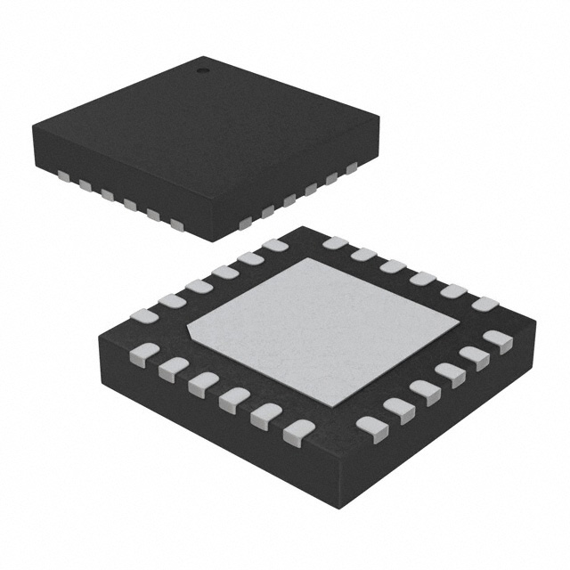
The MP6500 is available in QFN-24
(5mmx5mm) and TSSOP-28 EP packages.
Wide 4.5V to 35V Input Voltage Range
Two Internal Full-Bridge Drivers
Internal Current Sensing and Regulation
Low On Resistance (HS: 195mΩ, LS:
170mΩ)
No Control Power Supply Required
Simple Logic Interface
3.3V and 5V Compatible Logic Supply
Step Modes from Full-Step to Eighth-Step
2.5A Output Current
Automatic Current Decay
Over-Current Protection (OCP)
Input Over-Voltage Protection (OVP)
Thermal Shutdown and Under-Voltage
Lockout (UVLO) Protection
Fault Indication Output
Available in QFN-24 (5mmx5mm) and
Thermally Enhanced TSSOP-28 Packages
APPLICATIONS
Bipolar Stepper Motors
Printers
All MPS parts are lead-free, halogen-free, and adhere to the RoHS
directive. For MPS green status, please visit the MPS website under
Quality Assurance. “MPS” and “The Future of Analog IC Technology” are
registered trademarks of Monolithic Power Systems, Inc.
TYPICAL APPLICATION
MP6500
100nF
nFAULT
CPB
STEP
VCP
DIR
µC
CPA
nENBL
VIN
MS1
VG
MS2
nSLEEP
VIN
1µF
220
nF
AOUT1
AOUT2
ISET
BOUT1
ROSC
BOUT2
Step
Motor
GND
MP6500 Rev. 1.01
12/27/2017
www.MonolithicPower.com
MPS Proprietary Information. Patent Protected. Unauthorized Photocopy and Duplication Prohibited.
© 2017 MPS. All Rights Reserved.
1
�MP6500 – 35V, 2.5A, STEP MOTOR DRIVER W/ INTERNAL CURRENT SENSE
ORDERING INFORMATION
Part Number*
MP6500GF*
MP6500GU**
Package
TSSOP-28 EP
QFN-24 (5mmx5mm)
Top Marking
See Below
See Below
* For Tape & Reel, add suffix –Z (e.g. MP6500GF–Z)
** For Tape & Reel, add suffix –Z (e.g. MP6500GU–Z)
TOP MARKING
MPS: MPS prefix
YY: Year code
WW: Week code
MP6500: Part number
LLLLLLLLL: Lot number
TOP MARKING
MPS: MPS prefix
YY: Year code
WW: Week code
MP6500: Part number
LLLLLLL: Lot number
PACKAGE REFERENCE
nSLEEP
GND
VIN
22
AOUT2
AOUT1
TOP VIEW
19
23
20
24
21
GND
TOP VIEW
CP1
1
28
CP2
VG
2
27
NC
NC
3
26
NC
nENBL
4
25
VCP
nSLEEP
5
24
STEP
GND
6
23
GND
AOUT2
7
22
BOUT2
VIN
8
DIR
1
18
nENBL
nFAULT
2
17
VG
ISET
3
16
CP1
AGND
4
15
CP2
AOUT1
ROSC
5
14
VCP
GND
MS2
6
13
STEP
GND
BOUT2
VIN
GND
MS1
12
11
9
10
8
7
BOUT1
GND
QFN-24 (5mmx5mm)
MP6500 Rev. 1.01
12/27/2017
GND
GND
21
VIN
9
20
BOUT1
10
19
GND
DIR
11
18
MS1
nFAULT
12
17
NC
ISET
13
16
MS2
AGND
14
15
ROSC
TSSOP-28 EP
www.MonolithicPower.com
MPS Proprietary Information. Patent Protected. Unauthorized Photocopy and Duplication Prohibited.
© 2017 MPS. All Rights Reserved.
2
�MP6500 – 35V, 2.5A, STEP MOTOR DRIVER W/ INTERNAL CURRENT SENSE
ABSOLUTE MAXIMUM RATINGS (1)
Thermal Resistance
Supply voltage (VIN) ...................... -0.3V to 40V
xOUTx voltage (VA/BOUT1/2) .............. -0.7V to 40V
VCP, CPB .............................. VIN to VIN + 6.5V
All other pins to AGND .................. -0.3V to 6.5V
ESD rating (HBD) ........................................ 2kV
(2)
Continuous power dissipation (TA = +25°C)
QFN ...........................................................3.5W
TSSOP ......................................................3.9W
Storage temperature ................ -55°C to +150°C
Junction temperature ............................. +150°C
Lead temperature (solder) ..................... +260°C
QFN-25 (5mmx5mm) ............ 36 ........ 8 .... °C/W
TSSOP-28 EP ....................... 32 ........ 6 .... °C/W
Recommended Operating Conditions
(3)
Supply voltage (VIN) ....................... 4.5V to 35V
Output current (IA,BOUT) .............................. ±2.5A
Operating junction temp. (TJ). .. -40°C to +125°C
MP6500 Rev. 1.01
12/27/2017
(4)
θJA
θJC
NOTES:
1) Exceeding these ratings may damage the device.
2) The maximum allowable power dissipation is a function of the
maximum junction temperature TJ (MAX), the junction-toambient thermal resistance θJA, and the ambient temperature
TA. The maximum allowable continuous power dissipation at
any ambient temperature is calculated by PD (MAX) = (TJ
(MAX)-TA)/θJA. Exceeding the maximum allowable power
dissipation produces an excessive die temperature, causing
the regulator to go into thermal shutdown. Internal thermal
shutdown circuitry protects the device from permanent
damage.
3) The device is not guaranteed to function outside of its
operating conditions.
4) Measured on JESD51-7, 4-layer PCB.
www.MonolithicPower.com
MPS Proprietary Information. Patent Protected. Unauthorized Photocopy and Duplication Prohibited.
© 2017 MPS. All Rights Reserved.
3
�MP6500 – 35V, 2.5A, STEP MOTOR DRIVER W/ INTERNAL CURRENT SENSE
ELECTRICAL CHARACTERISTICS
VIN = 24V, TA = +25°C, unless otherwise noted.
Parameter
Power Supply
Input supply voltage
Quiescent current
Symbol
Condition
VIN
IQ
ISLEEP
Min
Typ
Max
Units
4.5
24
35
V
1.5
5
mA
1
µA
0.22
Ω
VIN = 24V, nENBL = 0,
nSLEEP = 1, with no load
VIN = 24V, nSLEEP = 0
Internal MOSFETs
RHS
Output on resistance
RLS
Body diode forward voltage
Control Logic
Input logic low threshold
Input logic high threshold
VF
VIN = 24V, IOUT = 1A,
TJ = 25°C
VIN = 24V, IOUT = 1A,
TJ = 85°C
VIN = 24V, IOUT = 1A,
TJ = 25°C
VIN = 24V, IOUT = 1A,
TJ = 85°C
IOUT = 1.5A
VIL
VIH
IIN(H)
VIH = 5V
Logic input current
IIN(L)
VIL = 0.8V
RPD
Internal pull-down resistance
Home nFAULT Outputs (Open-Drain Outputs)
Output low voltage
VOL
IO = 5mA
Output high leakage current
IOH
VO = 3.3V
Protection Circuit
VIN_RISE
UVLO rising threshold
Input OVP threshold
VOVP
Input OVP hysteresis
∆VOVP
IOCP1
Sinking
Over-current trip level
IOCP2
Sourcing
Over-current deglitch time
tOCP
(5)
TTSD
Thermal shutdown
Thermal shutdown hysteresis
∆TTSD
0.195
0.17
tOFF
IPEAK
VISET
AISET
tBLANK
Current trip accuracy
∆ITRIP
Rosc = 200kΩ
RISET = 71kΩ
IISET/IOUT
0.21
1.1
V
0.8
V
V
µA
µA
kΩ
2.1
20
5
500
36
3.5
3.5
3.4
37.5
1900
6
6
1
165
0.5
1
V
µA
4.5
38.5
V
V
mV
A
A
µs
°C
8.5
8.5
15
20
0.95
0.8
10
23
1.0
0.9
11.539
°C
26
1.05
1
13
2
RISET = 71kΩ, 71% - 100%
RISET = 71kΩ, 38% - 67%
RISET = 71kΩ,
end
tOFFof tOFF
IOUTITRIP
> Iat
at of
end
TRIP
In some cases, specifically high voltage and low
inductance or the regulation of very small
currents, the minimum on time of the PWM
cycle (set by the blanking time described above)
can cause the current to rise very quickly. In
this case, both slow and fast decay are used
(see Figure 4).
MP6500 Rev. 1.01
12/27/2017
SLEEP, nENBL Operation
Driving nSLEEP low puts the device into a lowpower sleep state. In this state, the gate drive
charge pump is stopped, and all the internal
circuits and H-bridge outputs are disabled. All
inputs are ignored when nSLEEP is active low.
When waking up from sleep mode,
approximately 1ms of time must pass before a
STEP command can be issued to allow the
internal circuitry to stabilize. nSLEEP has an
internal pull-down resistor.
www.MonolithicPower.com
MPS Proprietary Information. Patent Protected. Unauthorized Photocopy and Duplication Prohibited.
© 2017 MPS. All Rights Reserved.
13
�MP6500 – 35V, 2.5A, STEP MOTOR DRIVER W/ INTERNAL CURRENT SENSE
The nENBL pin is used to control the output
drivers. When nENBL is low, the output Hbridge outputs are enabled, and the rising
edges on STEP are recognized. When nENBL
is high, the H-bridge outputs are disabled, and
the STEP input is ignored. nENBL has an
internal pull-down resistor.
Fault Reporting
The MP6500 provides an nFAULT pin, which
reports if a fault condition (such as OCP, OTP,
or OVP) occurs. nFAULT is an open-drain
output and is driven low when a fault condition
occurs. If the fault condition is removed,
nFAULT is pulled high by an external pull-up
resistor.
Over-Current Protection (OCP)
Over-current protection (OCP) circuitry limits
the current through the MOSFETs by disabling
the gate driver. If the over-current limit
threshold is exceeded for longer than the overcurrent deglitch time, all MOSFETs in the Hbridge are disabled, and nFAULT is driven low.
The driver remains disabled for 2.4ms typically,
at which time it is re-enabled automatically.
Over-Voltage Protection (OVP)
If the input voltage on VIN is higher than the
over-voltage protection (OVP) threshold, the Hbridge output is disabled, and nFAULT is driven
low. This protection is released when VIN drops
below 36V.
Input
Under-Voltage
Lockout
(UVLO)
Protection
If at any time the voltage on VIN falls below the
under-voltage lockout (UVLO) threshold voltage,
all circuitry in the device is disabled, and the
internal logic is reset. Operation resumes when
VIN rises above the UVLO threshold.
Thermal Shutdown
If the die temperature exceeds safe limits, all
MOSFETs in the H-bridge are disabled, and
nFAULT is driven low. Once the die
temperature has fallen to a safe level, operation
resumes automatically.
Over-current conditions on both high- and lowside devices (i.e.: a short to ground, supply, or
across the motor winding) result in an overcurrent shutdown. Note that OCP does not use
the current sense circuitry used for PWM
current control.
MP6500 Rev. 1.01
12/27/2017
www.MonolithicPower.com
MPS Proprietary Information. Patent Protected. Unauthorized Photocopy and Duplication Prohibited.
© 2017 MPS. All Rights Reserved.
14
�MP6500 – 35V, 2.5A, STEP MOTOR DRIVER W/ INTERNAL CURRENT SENSE
MICROSTEPPING
Table 2: Relative Current Level Sequence
Eighth Step
#
Quarter Step
#
Half Step
#
1
2
3
4
5
6
7
8
9
10
11
12
13
14
15
16
17
18
19
20
21
22
23
24
25
26
27
28
29
30
31
32
1
1
MP6500 Rev. 1.01
12/27/2017
Full Step
#
2
3
2
1
4
5
3
6
7
4
2
8
9
5
10
11
6
3
12
13
7
14
15
16
8
4
Phase A
Current %ITripLIMIT (%)
Phase B
Current %ITRIP
-LIMIT (%)
Step
Angle (°)
100.00
98.08
92.39
83.15
70.71
55.56
38.27
19.51
0.00
-19.51
-38.27
-55.56
-70.71
-83.15
-92.39
-98.08
-100.00
-98.08
-92.39
-83.15
-70.71
-55.56
-38.27
-19.51
0.00
19.51
38.27
55.56
70.71
83.15
92.39
98.08
0.00
19.51
38.27
55.56
70.71
83.15
92.39
98.08
100.00
98.08
92.39
83.15
70.71
55.56
38.27
19.51
0.00
-19.51
-38.27
-55.56
-70.71
-83.15
-92.39
-98.08
-100.00
-98.08
-92.39
-83.15
-70.71
-55.56
-38.27
-19.51
0.0
11.3
22.5
33.8
45.0
56.3
67.5
78.8
90.0
101.3
112.5
123.8
135.0
146.3
157.5
168.8
180.0
191.3
202.5
213.8
225.0
236.3
247.5
258.8
270.0
281.3
292.5
303.8
315.0
326.3
337.5
348.8
www.MonolithicPower.com
MPS Proprietary Information. Patent Protected. Unauthorized Photocopy and Duplication Prohibited.
© 2017 MPS. All Rights Reserved.
15
�MP6500 – 35V, 2.5A, STEP MOTOR DRIVER W/ INTERNAL CURRENT SENSE
MICROSTEPPING (continued)
Figure 5a: Full Step (4 Step Sequences)
Figure 5b: Half Step (8 Step Sequences)
MP6500 Rev. 1.01
12/27/2017
www.MonolithicPower.com
MPS Proprietary Information. Patent Protected. Unauthorized Photocopy and Duplication Prohibited.
© 2017 MPS. All Rights Reserved.
16
�MP6500 – 35V, 2.5A, STEP MOTOR DRIVER W/ INTERNAL CURRENT SENSE
MICROSTEPPING (continued)
Figure 5c: Quarter Step (16 Step)
Figure 5d: Eighth Step (32 Step)
MP6500 Rev. 1.01
12/27/2017
www.MonolithicPower.com
MPS Proprietary Information. Patent Protected. Unauthorized Photocopy and Duplication Prohibited.
© 2017 MPS. All Rights Reserved.
17
�MP6500 – 35V, 2.5A, STEP MOTOR DRIVER W/ INTERNAL CURRENT SENSE
PACKAGE INFORMATION
QFN-24 (5mmx5mm)
PIN 1 ID
0.30x45° TYP.
PIN 1 ID
MARKING
PIN 1 ID INDEX
AREA
BOTTOM VIEW
TOP VIEW
SIDE VIEW
NOTE:
1) ALL DIMENSIONS ARE IN MILLIMETERS.
2) EXPOSED PADDLE SIZE DOES NOT
INCLUDE MOLD FLASH.
3) LEAD COPLANARITY SHALL BE 0.10
MILLIMETERS MAX.
4) DRAWING CONFIRMS TO JEDEC MO-220.
5) DRAWING IS NOT TO SCALE.
RECOMMENDED LAND PATTERN
MP6500 Rev. 1.01
12/27/2017
www.MonolithicPower.com
MPS Proprietary Information. Patent Protected. Unauthorized Photocopy and Duplication Prohibited.
© 2017 MPS. All Rights Reserved.
18
�MP6500 – 35V, 2.5A, STEP MOTOR DRIVER W/ INTERNAL CURRENT SENSE
PACKAGE
INFORMATION (continued)
PACKAGE OUTLINE DRAWING FOR 28-TSSOP w/ EXPOSED PADDLE
TSSOP-28
EP
MF-PO-D-0055
revision
2.0
6.00
TYP
9.60
9.80
0.65
BSC
0.40
TYP
28
15
1.60
TYP
4.30
4.50
PIN 1 ID
3.20
TYP
6.20
6.60
5.80
TYP
14
1
TOP VIEW
RECOMMENDED LAND PATTERN
0.80
1.05
1.20 MAX
SEATING PLANE
0.19
0.30
0.65 BSC
0.00
0.15
0.09
0.20
SEE DETAIL "A"
FRONT VIEW
SIDE VIEW
GAUGE PLANE
0.25 BSC
5.40
5.90
0o-8o
0.45
0.75
DETAIL “A”
2.60
3.10
BOTTOM VIEW
NOTE:
1) ALL DIMENSIONS ARE IN MILLIMETERS.
2) PACKAGE LENGTH DOES NOT INCLUDE MOLD FLASH,
PROTRUSION OR GATE BURR.
3) PACKAGE WIDTH DOES NOT INCLUDE INTERLEAD FLASH
OR PROTRUSION.
4) LEAD COPLANARITY (BOTTOM OF LEADS AFTER FORMING)
SHALL BE 0.10 MILLIMETERS MAX.
5) DRAWING CONFORMS TO JEDEC MO-153, VARIATION AET.
6) DRAWING IS NOT TO SCALE.
NOTICE: The information in this document is subject to change without notice. Please contact MPS for current specifications.
Users should warrant and guarantee that third party Intellectual Property rights are not infringed upon when integrating MPS
products into any application. MPS will not assume any legal responsibility for any said applications.
MP6500 Rev. 1.01
12/27/2017
www.MonolithicPower.com
MPS Proprietary Information. Patent Protected. Unauthorized Photocopy and Duplication Prohibited.
© 2017 MPS. All Rights Reserved.
19
�