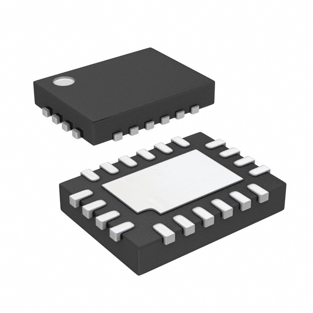
MP6515
35V, 2.8A, Phase/Enable Control
H-Bridge Motor Driver
in QFN 3x4 and TSSOP-EP Packages
The Future of Analog IC Technology
DESCRIPTION
The MP6515 is an H-bridge motor driver. It
operates from a supply voltage of up to 35V
and delivers motor current up to 2.8A. Typically,
the MP6515 is used to drive a DC brush motor.
For the MP6515, control of the outputs is
accomplished through the PHASE, ENBL,
BRAKE, and BMODE pins.
An internal current sensing circuit provides an
output with voltage proportional to the load
current. In addition, cycle-by-cycle current
regulation/limiting is provided. These features
do not require the use of a low-ohm shunt
resistor.
Internal safety features include over-current
protection, input over-voltage protection, undervoltage lockout (UVLO), and thermal shutdown.
The
MP6515
is
available
in
16-pin
5.0mmx6.4mm TSSOP-EP and 3mmx4mm
QFN package with exposed thermal pad.
FEATURES
Wide 5.4V to 35V Input Voltage Range
2.8A Peak Output Current
Internal Full H-Bridge Driver
PHASE/ENABLE control, input logic
(PHASE, EN, BRAKE, BMODE)
Cycle-by-Cycle Current Regulation/Limit
Low On Resistance (HS:250mΩ;LS:250mΩ)
Simple, Versatile Logic Interfaces
3.3V and 5V Compatible Logic Supply
Over-Current Protection
Over-Voltage Protection
Thermal Shutdown
Under-Voltage Lockout
Fault Indication Output
Thermally
Enhanced
Surface-Mount
Package
APPLICATIONS
Solenoid Drivers
DC Brush Motor Drive
All MPS parts are lead-free, halogen free, and adhere to the RoHS directive. For
MPS green status, please visit MPS website under Quality Assurance. “MPS”
and “The Future of Analog IC Technology” are Registered Trademarks of
Monolithic Power Systems, Inc.
TYPICAL APPLICATION
MP6515 Rev. 1.03
3/21/2019
www.MonolithicPower.com
MPS Proprietary Information. Patent Protected. Unauthorized Photocopy and Duplication Prohibited.
© 2019 MPS. All Rights Reserved.
1
�MP6515 – 35V, 2.8A, PHASE/ENABLE CONTROL, H-BRIDGE MOTOR DRIVER
ORDERING INFORMATION
Part Number*
MP6515GF*
MP6515GL**
Package
TSSOP-16 EP (5.0mm × 6.4mm)
QFN-20 (3mm x 4mm)
Top Marking
See Below
See Below
* For Tape & Reel, add suffix –Z (e.g. MP6515GF–Z)
** For Tape & Reel, add suffix –Z (e.g. MP6515GL–Z)
TOP MARKING (TSSOP-16EP)
MPS: MPS prefix
YY: Year code
WW: Week code
MP6515: Part number
LLLLLL: Lot number
TOP MARKING (QFN-20)
MP: MPS prefix
Y: Year code
W: Week code
6515: First four digits of the part number
LLL: Lot number
MP6515 Rev. 1.03
3/21/2019
www.MonolithicPower.com
MPS Proprietary Information. Patent Protected. Unauthorized Photocopy and Duplication Prohibited.
© 2019 MPS. All Rights Reserved.
2
�MP6515 – 35V, 2.8A, PHASE/ENABLE CONTROL, H-BRIDGE MOTOR DRIVER
PACKAGE REFERENCE
TSSOP-16 EP (5.0mm × 6.4mm)
ABSOLUTE MAXIMUM RATINGS (1)
Supply voltage (VIN) ....................... –0.3V to 40V
OUTx voltage (VOUT1/2) .................... -0.7V to 40V
VCP, CPB ................................... VIN to VIN+6.5V
ESD Rating (HBD) ........................................ 2kV
ISET ............................................... -0.3V to 4.5V
All other pins to GND ..................... -0.3V to 6.5V
Continuous power dissipation (TA = +25°C) (2)
TSSOP-16 EP……………………………...2.77W
QFN-20 (3mmx4mm)……………….…….2.60W
Storage temperature .................-55C to +150C
Junction temperature .............................. +150C
Lead temperature (solder) ...................... +260C
Recommended Operating Conditions (3)
Supply voltage (VIN) ......................... 5.4V to 35V
Continuous output current (IOUT) ............ ±1.5A(4)
Load current (IVISEN) ................................... ±2mA
Operating junction temp. (TJ). ...-40°C to +125°C
MP6515 Rev. 1.03
3/21/2019
QFN-20 (3mm x 4mm)
Thermal Resistance (5)
θJA
θJC
TSSOP-16 EP .................... 45 ...... 10 C/W
QFN-20 (3mmx4mm)............. 48 ....... 10 C/W
Notes:
1) Exceeding these ratings may damage the device.
2) The maximum allowable power dissipation is a function of the
maximum junction temperature TJ (MAX), the junction-toambient thermal resistance θJA, and the ambient temperature
TA. The maximum allowable continuous power dissipation at
any ambient temperature is calculated by PD (MAX) = (TJ
(MAX)-TA)/θJA. Exceeding the maximum allowable power
dissipation will cause excessive die temperature, and the
regulator will go into thermal shutdown. Internal thermal
shutdown circuitry protects the device from permanent
damage.
3) The device is not guaranteed to function outside of its
operating conditions.
4) Continuous current depends on PCB layout and ambient
temperature.
5) Measured on JESD51-7, 4-layer PCB
www.MonolithicPower.com
MPS Proprietary Information. Patent Protected. Unauthorized Photocopy and Duplication Prohibited.
© 2019 MPS. All Rights Reserved.
3
�MP6515 – 35V, 2.8A, PHASE/ENABLE CONTROL, H-BRIDGE MOTOR DRIVER
ELECTRICAL CHARACTERISTICS
VIN=24V, TA = +25°C, unless otherwise noted.
Parameter
Power Supply
Input supply voltage
Quiescent current
Charge pump frequency
Internal MOSFETs
Symbol
VIN
IQ
ISLEEP
fCP
RHS
Output on resistance
RLS
Body diode forward voltage
Control Logic
Input logic ‘low’ threshold
Input logic ‘high’ threshold
VF
VIL
VIH
IIN(H)
Logic input current
IIN(L)
RPD
Internal pull-down resistance
nFault Output (Open-Drain Output)
Output low voltage
VOL
Output high leakage current
IOH
Protection Circuits
VIN_RISE
UVLO rising threshold
VHYS
UVLO hysteresis
VOVP
Input OVP threshold
∆VOVP
Input OVP hysteresis
IOCP1
Over-current trip level
IOCP2
tOCPD
Over-current deglitch time(6)
tOCP
Over-current retry time
TTSD
Thermal shutdown
∆TTSD
Thermal shutdown hysteresis
MP6515 Rev. 1.03
3/21/2019
Condition
Min
Typ
Max
Units
5.4
24
35
V
1.5
2
mA
1
µA
kHz
0.3
Ω
VIN = 24V; nSLEEP = 1
No load current
VIN = 24V; nSLEEP = 0
680
VIN = 24V, IOUT = 1A,
TJ = 25°C
VIN = 24V, IOUT = 1A,
TJ = 85°C
VIN = 24V, IOUT = 1A,
TJ = 25°C
VIN = 24V, IOUT = 1A,
TJ = 85°C
IOUT = 1.5A
VIH = 5V
VIL = 0.8V
0.25
0.3
0.25
Ω
0.3
0.3
Ω
1.1
V
0.8
V
V
µA
µA
kΩ
2
-20
-20
20
20
515
IO = 5mA
VO = 3.3V
36
Sinking
Sourcing
3.2
3.2
5
310
38
2000
4
4
500
0.9
165
30
Ω
0.5
1
V
µA
5.3
V
mV
V
mV
A
A
ns
ms
oC
oC
www.MonolithicPower.com
MPS Proprietary Information. Patent Protected. Unauthorized Photocopy and Duplication Prohibited.
© 2019 MPS. All Rights Reserved.
40
5
5
4
�MP6515 – 35V, 2.8A, PHASE/ENABLE CONTROL, H-BRIDGE MOTOR DRIVER
ELECTRICAL CHARACTERISTICS
VIN=24V, TA = +25°C, unless otherwise noted.
Parameter
Current Control
Off time
ISET current
Current trip voltage (rising)
Current trip voltage (falling)
VISEN output
Output voltage accuracy
Symbol
Condition
tITRIP
IISET
VITRIP-R
VITRIP-F
After ITRIP
At VISEN pin
At VISEN pin
∆VVISEN
VISET > 0.5V
Min
Typ
90
1.44
1.15
16
100
1.5
1.2
Max
Units
110
1.56
1.25
µs
µA/A
V
V
5
%
-5
6) Guarantee by design
MP6515 Rev. 1.03
3/21/2019
www.MonolithicPower.com
MPS Proprietary Information. Patent Protected. Unauthorized Photocopy and Duplication Prohibited.
© 2019 MPS. All Rights Reserved.
5
�MP6515 – 35V, 2.8A, PHASE/ENABLE CONTROL, H-BRIDGE MOTOR DRIVER
TYPICAL CHARACTERISTICS
300
250
250
200
200
150
150
100
100
50
0
0
50
0.5
1
1.5
2
0
2.5
1.22
1.215
105
1.53
104
1.525
103
102
1.52
101
1.515
100
99
1.51
98
97
96
-50
1.505
-20
10
40
70 100 130
340
360
320
340
1.19
-50
-20
10
MP6515 Rev. 1.03
3/21/2019
40
70 100 130
-20
10
40
70 100 130
240
220
220
200
200
180
-50
70 100 130
260
240
1.195
40
280
260
1.2
10
300
280
1.205
-20
320
300
1.21
1.5
-50
-20
10
40
70 100 130
180
-50
www.MonolithicPower.com
MPS Proprietary Information. Patent Protected. Unauthorized Photocopy and Duplication Prohibited.
© 2019 MPS. All Rights Reserved.
6
�MP6515 – 35V, 2.8A, PHASE/ENABLE CONTROL, H-BRIDGE MOTOR DRIVER
TYPICAL PERFORMANCE CHARACTERISTICS
VIN = 24V, IOUT = 1A, TA = 25°C, unless otherwise noted.
VOUT
20V/div.
VISET
1V/div.
VISEN
1V/div.
IOUT
1A/div.
VIN
10V/div.
VIN
10V/div.
VISEN
500mV/div.
VOUT
10V/div.
VISEN
500mV/div.
VOUT
10V/div.
IOUT
500mA/div.
IOUT
500mA/div.
VnFAULT
1V/div.
VnSLEEP
2V/div.
VnSLEEP
2V/div.
VISEN
500mV/div.
VISEN
500mV/div.
VOUT
10V/div.
VOUT
10V/div.
IOUT
500mA/div.
IOUT
500mA/div.
VnFAULT
1V/div.
VnFAULT
1V/div.
VOUT1
20V/div.
VOUT2
20V/div.
VOUT1
20V/div.
VOUT1
20V/div.
VOUT2
20V/div.
IOUT
5A/div.
VOUT2
20V/div.
IOUT
5A/div.
MP6515 Rev. 1.03
3/21/2019
IOUT
5A/div.
www.MonolithicPower.com
MPS Proprietary Information. Patent Protected. Unauthorized Photocopy and Duplication Prohibited.
© 2019 MPS. All Rights Reserved.
7
�MP6515 – 35V, 2.8A, PHASE/ENABLE CONTROL, H-BRIDGE MOTOR DRIVER
PIN FUNCTIONS
TSSOP16
Pin #
QFN20
Pin #
Name
1
20
nFAULT
2
3
4, 13
1
2
3, 14
BRAKE
PHASE
GND
5
4
nSLEEP
6
7
5
6
ENBL
OUT1
8
7
ISET
9
8, 9, 10
VIN
10
11
12
14
15
16
EP
11
12
13
15
16
17
18, 19
EP
OUT2
CPA
CPB
VCP
VISEN
BMODE
NC
GND
MP6515 Rev. 1.03
3/21/2019
Description
Fault indication. Open-drain output, logic low when in fault condition
(OCP, OTP, OVP).
Brake input. Internal pulldown.
H-bridge phase input (motor direction). Internal pulldown.
System ground connection.
Sleep mode input. Logic low to enter low-power sleep mode. Internal
pulldown.
H-bridge enable input. High to enable H-bridge. Internal pulldown.
Output terminal 1.
Current programming resistor. Connect a resistor to ground to set
the current limit and VISEN output voltage.
Input supply voltage. Decouple to GND with a minimum 100nF
ceramic capacitor to GND.
Output terminal 2.
Charge pump flying capacitor. Connect a 100nF ceramic capacitor
between CPA and CPB.
Charge pump output. Connect a 100nF capacitor to VIN.
Current sense output voltage.
Brake mode. Internal pulldown.
No connection.
The exposed pad MUST be connected to ground.
www.MonolithicPower.com
MPS Proprietary Information. Patent Protected. Unauthorized Photocopy and Duplication Prohibited.
© 2019 MPS. All Rights Reserved.
8
�MP6515 – 35V, 2.8A, PHASE/ENABLE CONTROL, H-BRIDGE MOTOR DRIVER
BLOCK DIAGRAM
VIN
MP6515
VIN
VCP
Charge
Pump
UVLO
OVP
OTS
VREF
Int. VCC
LS Gate Drive V
Gate
Driver
PHASE
µC
BMODE
CPB
OUT1
nFAULT
ENBL
BRAKE
VIN
CPA
OUT2
Control
Logic
SLEEP
Curr.
Reg.
ISENSE
VISEN
ITRIP
GND
+
-
1.5V
RISET
Figure 1: Functional Block Diagram
MP6515 Rev. 1.03
3/21/2019
www.MonolithicPower.com
MPS Proprietary Information. Patent Protected. Unauthorized Photocopy and Duplication Prohibited.
© 2019 MPS. All Rights Reserved.
9
�MP6515 – 35V, 2.8A, PHASE/ENABLE CONTROL, H-BRIDGE MOTOR DRIVER
OPERATION
The MP6515 is an H-bridge motor driver, which
integrates four N-channel power MOSFETs with
2.8A peak current capability. It operates over a
wide input voltage range of 5.4V to 35V. It is
designed to drive bipolar stepper motors, DC
brush motors, solenoids, or other loads.
Current Sensing
The current flowing in the two low-side
MOSFETs is sensed with an internal current
sensing circuit. A voltage that is proportional to
the output current is sourced on VISEN.
The VISEN output voltage scaling is set by a
resistor connected between ISET and ground.
For 1A of output current, 100µA of current is
sourced into the resistor connected to ISET. For
example, if a 10kΩ resistor is connected
between ISET and ground, the output voltage
on VISEN will be 1V/A of output current.
Current is sensed when one of the low-side
MOSFETs is turned on, including during slow
decay (brake) mode.
The load current applied to VISEN should be
kept below 2mA, with no more than 500pF of
capacitance.
Current Limit/Regulation
The current in the outputs is limited using
constant off-time pulse width modulation (PWM)
control circuitry. Operation is as follows:
MP6515 Rev. 1.03
3/21/2019
Initially, a diagonal pair of MOSFETs
turns on and drives current through the
load.
The current increases in the load, which
is sensed by the internal current sense
circuit.
If the load current reaches the current
trip threshold, the H-bridge switches to
slow decay mode, with the two low-side
MOSFETs turned on.
After a fixed off-time (tITRIP), if the load
current falls at least 20% below the
current limit threshold, the FETs are reenabled and the cycle repeats.
If the current is still higher than this level,
the off time is extended until the current
falls to 20% below the current limit
threshold.
The current limit threshold is reached when
VISEN reaches 1.5V. For example, with a 10kΩ
resistor from ISET to ground, the VISEN
voltage is 1V/A of output current. Thererfore,
when the current reaches 1.5A, VISET voltage
reaches 1.5V, and a current trip occurs.
During current regulation, nFAULT is not
activated. See below:
www.MonolithicPower.com
MPS Proprietary Information. Patent Protected. Unauthorized Photocopy and Duplication Prohibited.
© 2019 MPS. All Rights Reserved.
10
�MP6515 – 35V, 2.8A, PHASE/ENABLE CONTROL, H-BRIDGE MOTOR DRIVER
Blanking Time
There is often a current spike during the turn-on,
due to the body diode’s reverse-recovery
current or the shunt capacitance of the load.
This current spike requires filtering to prevent it
from erroneously shutting down the high-side
MOSFET. An internal fixed blanking time (tOCPD)
blanks the output of the current sense
comparator when the outputs are switched.
This blanking time also sets the minimum on
time for the high-side MOSFET.
Input Logic
For the MP6515, control of the outputs is
accomplished through the PHASE, ENBL,
BRAKE, and BMODE pins. See Table 1:
Table 1: Output Control Pins
ENBL PHASE BRAKE BMODE OUT1 OUT2 Function
1
0
X
L
H Reverse
X
1
1
X
H
L Forward
X
0
X
1
L
L Brake (low)
0
0
X
1
H
H Brake (high)
1
0
0
0
H*
L* Sync fast decay
X
0
1
0
X
L*
H* Sync fast decay
* As the current through the H-bridge approaches
zero, the outputs are tri-stated
nSLEEP Operation
Driving nSLEEP low puts the device into a low
power sleep state. In this state, all internal
circuits, including the gate drive charge pump,
are disabled, and the H-bridge outputs are
turned off. All inputs are ignored when nSLEEP
is active low. When waking up from sleep mode,
time (approximately 1ms) must pass before the
outputs will operate.
Fault
The MP6515 provides an nFAULT pin, which is
driven active low if any of the protection circuits
are activated. These fault conditions include
over-current, over-temperature, and overvoltage. nFAULT is not driven low when a
current limit trip occurs. nFAULT is an opendrain output and requires an external pull-up
resistor. When the fault condition is removed,
nFAULT is pulled inactive high by the pull-up
resistor.
MP6515 Rev. 1.03
3/21/2019
Over-Current Protection
The over-current protection circuit limits the
current through each FET by reducing the gate
drive to the FET. If the FET remains in the
current limit condition for longer than the overcurrent deglitch time, all MOSFETs in the Hbridge will be disabled, and nFAULT will be
driven low. The driver will remain disabled for
tOCP, at which point it will be re-enabled
automatically. Over-current conditions are
sensed on both high and low side devices; i.e.,
a short to ground, supply, or across the motor
winding will result in an over-current shutdown.
Note that over-current protection does not use
the current sense circuitry used for PWM
current control, and it is independent of the
ISET resistor value.
Over-Voltage Protection
If the input voltage applied to VIN is higher than
the OVP threshold, the H-bridge output will be
disabled, and nFAULT will be driven low. This
protection is released when VIN drops to a safe
level.
Input UVLO Protection
If at any time the voltage on VIN falls below the
under-voltage lockout threshold, all circuitry in
the device will be disabled and the internal logic
will be reset. Operation will resume when VIN
rises above the UVLO threshold.
Thermal Shutdown
If the die temperature exceeds safe limits, all
MOSFETs in the H-bridge will be disabled, and
nFAULT will be driven low. Once the die
temperature has fallen to a safe level, operation
will resume automatically.
www.MonolithicPower.com
MPS Proprietary Information. Patent Protected. Unauthorized Photocopy and Duplication Prohibited.
© 2019 MPS. All Rights Reserved.
11
�MP6515 – 35V, 2.8A, PHASE/ENABLE CONTROL, H-BRIDGE MOTOR DRIVER
PACKAGE INFORMATION
TSSOP16-EP (5.0×6.4mm)
PIN 1 ID
TOP VIEW
RECOMMENDED LAND PATTERN
SEE DETAIL "A"
FRONT VIEW
SIDE VIEW
DETAIL "A"
NOTE:
BOTTOM VIEW
MP6515 Rev. 1.03
3/21/2019
1) ALL DIMENSIONS ARE IN MILLIMETERS.
2) PACKAGE LENGTH DOES NOT INCLUDE MOLD
FLASH, PROTRUSION OR GATE BURR.
3) PACKAGE WITDH DOES NOT INCLUDE INTERLEAD
FLASH OR PROTRUSION.
4) LEAD COPLANARITY (BOTTOM OF LEADS AFTER
FORMING) SHALL BE 0.10 MILLIMETERS MAX.
5) DRAWING CONFORMS TO JEDEC MO-153,
VARIATION ABT.
6) DRAWING IS NOT TO SCALE.
www.MonolithicPower.com
MPS Proprietary Information. Patent Protected. Unauthorized Photocopy and Duplication Prohibited.
© 2019 MPS. All Rights Reserved.
12
�MP6515 – 35V, 2.8A, PHASE/ENABLE CONTROL, H-BRIDGE MOTOR DRIVER
PACKAGE INFORMATION
QFN-20 (3mmx4mm)
PIN 1 ID
SEE DETAIL A
PIN 1 ID
MARKING
PIN 1 ID
INDEX AREA
BOTTOM VIEW
TOP VIEW
PIN 1 ID OPTION A
0.30x45° TYP.
PIN 1 ID OPTION B
R0.20 TYP.
DETAIL A
SIDE VIEW
NOTE:
1) ALL DIMENSIONS ARE IN MILLIMETERS.
2) EXPOSED PADDLE SIZE DOES NOT INCLUDE
MOLD FLASH.
3) LEAD COPLANARITY SHALL BE 0.10
MILLIMETERS MAX.
4) JEDEC REFERENCE IS MO-220.
5) DRAWING IS NOT TO SCALE.
RECOMMENDED LAND PATTERN
NOTICE: The information in this document is subject to change without notice. Users should warrant and guarantee that third
party Intellectual Property rights are not infringed upon when integrating MPS products into any application. MPS will not
assume any legal responsibility for any said applications.
MP6515 Rev. 1.03
3/21/2019
www.MonolithicPower.com
MPS Proprietary Information. Patent Protected. Unauthorized Photocopy and Duplication Prohibited.
© 2019 MPS. All Rights Reserved.
13
�