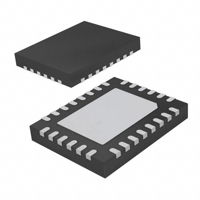
MP6520
8V to 32V, 1.5A, Stepper Motor Driver
with Integrated MOSFETs
DESCRIPTION
FEATURES
The MP6520 is a stepper motor driver with a
built-in microstepping translator. The MP6520
operates from a supply voltage of up to 32V
and can deliver a motor current of up to 1.5A.
The MP6520 can operate a bipolar stepper
motor in full-, half-, quarter-, and eighth-step
modes.
The MP6520 has a fixed 3.3V reference output,
which allows it to operate without a separate
logic power supply.
Full protection features include over-current
protection (OCP), input over-voltage protection
(OVP), under-voltage lockout (UVLO), and
thermal shutdown.
The MP6520 is available in a QFN-28
(4mmx5mm) package with an exposed thermal
pad.
Wide 8V to 32V Input Voltage Range
Two Internal Full-Bridge Drivers
Low On Resistance (HS: 300mΩ; LS:
300mΩ)
No Control Power Supply Required
Simple Logic Interface
Compatible with 3.3V and 5V Logic
Full-, Half-, Quarter-, and Eighth-Step
Functionality
1.5A Maximum Output Current
Adjustable Mixed Decay Ratio
Over-Current Protection (OCP)
Input Over-Voltage Protection (OVP)
Function
Thermal Shutdown and Under-Voltage
Lockout (UVLO) Protection
Fault Indication Output
Available in a QFN-28 (4mmx5mm)
Package
APPLICATIONS
Bipolar Stepper Motors
Printers
All MPS parts are lead-free, halogen-free, and adhere to the RoHS directive. For
MPS green status, please visit the MPS website under Quality Assurance.
“MPS” and “The Future of Analog IC Technology” are registered trademarks of
Monolithic Power Systems, Inc.
TYPICAL APPLICATION
3.3V
MP6520
0.47uF
VIN
CPA
3P3VOUT
CPB
100nF
VCP
nFAULT
VIN
nHOME
1uF
VG
1uF
STEP
DIR
MS1
MS2
µC
nENBL
nSLEEP
AOUT1
Exposed
GND PAD
AOUT2
SENA
SENA
nRSET
BOUT1
VREF
BOUT2
MDS
SENB
ROSC
200k
Ω
MP6520 Rev. 1.0
10/10/2016
Motor
SENB
GND
www.MonolithicPower.com
MPS Proprietary Information. Patent Protected. Unauthorized Photocopy and Duplication Prohibited.
© 2016 MPS. All Rights Reserved.
1
�MP6520 – 32V, 1.5A, MICROSTEPPING MOTOR DRIVER W/ INTEGRATED MOSFETS
ORDERING INFORMATION
Part Number*
MP6520GV
Package
QFN-28 (4mmx5mm)
Top Marking
See Below
* For Tape & Reel, add suffix –Z (e.g. MP6520GV–Z)
TOP MARKING
MPS: MPS prefix
Y: Year code
WW: Week code
MP6520: Part number
LLLLLL: Lot number
PACKAGE REFERENCE
GND
VCP
CPB
CPA
3P3VOUT
VREF
28
27
26
25
24
23
TOP VIEW
VIN
1
22
MDS
AOUT1
2
21
ROSC
SENA
3
20
nHOME
SENA
4
19
nFAULT
AOUT2
5
18
STEP
BOUT2
6
17
DIR
SENB
7
16
MS1
SENB
8
15
MS2
9
10
11
12
13
14
VIN
nSLEEP
VG
nRSET
nENBL
EXPOSED PAD ON
BACKSIDE
CONNECTED TO GND
BOUT1
MP6520
QFN-28 (4mmx5mm)
MP6520 Rev. 1.0
10/10/2016
www.MonolithicPower.com
MPS Proprietary Information. Patent Protected. Unauthorized Photocopy and Duplication Prohibited.
© 2016 MPS. All Rights Reserved.
2
�MP6520 – 32V, 1.5A, MICROSTEPPING MOTOR DRIVER W/ INTEGRATED MOSFETS
ABSOLUTE MAXIMUM RATINGS (1)
Thermal Resistance (4)
Supply voltage (VIN) ...................... -0.3V to 40V
xOUTx voltage (VA/BOUT1/2) .............. -0.7V to 40V
VCP, CPB .............................. VIN to VIN + 6.5V
ESD rating (HBD) ........................................ 2kV
SENA, SENB .......................................... 700mV
All other pins to AGND (except for 3P3VOUT
and VG) ........................................ -0.3V to 6.5V
Continuous power dissipation (TA = +25°C) (2)
..................................................................3.1W
Storage temperature ................ -55°C to +150°C
Junction temperature ............................. +150°C
Lead temperature (solder) ..................... +260°C
QFN-28 (4mmx5mm) ............ 40 ........ 9 .... °C/W
θJA
θJC
NOTES:
1) Exceeding these ratings may damage the device.
2) The maximum allowable power dissipation is a function of the
maximum junction temperature TJ (MAX), the junction-toambient thermal resistance θJA, and the ambient temperature
TA. The maximum allowable continuous power dissipation at
any ambient temperature is calculated by PD (MAX) = (TJ
(MAX)-TA)/θJA. Exceeding the maximum allowable power
dissipation produces an excessive die temperature, causing
the regulator to go into thermal shutdown. Internal thermal
shutdown circuitry protects the device from permanent
damage.
3) The device is not guaranteed to function outside of its
operating conditions.
4) Measured on JESD51-7, 4-layer PCB.
Recommended Operating Conditions (3)
Supply voltage (VIN) .......................... 8V to 32V
Output current (IA,BOUT) .............................. ±1.5A
Operating junction temp. (TJ). .. -40°C to +125°C
MP6520 Rev. 1.0
10/10/2016
www.MonolithicPower.com
MPS Proprietary Information. Patent Protected. Unauthorized Photocopy and Duplication Prohibited.
© 2016 MPS. All Rights Reserved.
3
�MP6520 – 32V, 1.5A, MICROSTEPPING MOTOR DRIVER W/ INTEGRATED MOSFETS
ELECTRICAL CHARACTERISTICS
VIN = 24V, TA = +25°C, unless otherwise noted.
Parameter
Power Supply
Input supply voltage
Quiescent current
Voltage Regulator
3P3VOUT reference output
Internal MOSFETs
Symbol
VIN
ISLEEP
VIN = 24V, nENBL = 0,
nSLEEP = 1, with no load
VIN = 24V, nSLEEP = 0
V3P3
IOUT = 1mA
IQ
RHS
Output on resistance
RLS
Body diode forward voltage
Control Logic
Input logic low threshold
Input logic high threshold
Condition
VF
Min
Typ
Max
Units
8
24
32
V
7
10
mA
5
µA
3.3
3.45
V
0.30
0.32
0.30
0.32
0.35
Ω
Ω
Ω
Ω
V
3.2
VIN = 24V, IOUT = 1A, TJ = 25°C
VIN = 24V, IOUT = 1A, TJ = 85°C
VIN = 24V, IOUT = 1A, TJ = 25°C
VIN = 24V, IOUT = 1A, TJ = 85°C
IOUT = 1.5A
VIL
All logic pins
VIH
All logic pins
IIN(H)
VIH = 5V
Logic input current
IIN(L)
VIL = 0.8V
RPD
All logic pins
Internal pull-down resistance
Home, nFault Outputs (Open-Drain Outputs)
VOL
IO = 5mA
Output low voltage
Output high leakage current
IOH
VO = 3.3V
Protection Circuit
VIN_RISE
UVLO rising threshold
(5)
VHYS
UVLO hysteresis
VOVP
Input OVP threshold
∆VOVP
Input OVP hysteresis
IOCP1
Sinking
Over-current trip level
IOCP2
Sourcing
Over-current deglitch time (5)
tOCP
TTSD
Thermal shutdown (5)
∆TTSD
Thermal shutdown hysteresis (5)
Current Control
tOFF
Constant off time
Rt = 200kΩ
tBLANK
Blanking time
HS off to LS on, or LS off to HS
Crossover dead time
tDT
on
IREF
VREF = 3.3V
VREF input current
VREF = 3.3V, 100% (no switch in
VTRIP
SENx trip voltage
test mode)
VREF = 3.3V, 70% - 100%
VREF = 3.3V, 38% - 64%
∆ITRIP
Current trip accuracy
VREF = 3.3V, 19% - 30%
VREF = 3.3V,
