MP7748
2x20W Stereo Single Ended
Class D Audio Amplifier
The Future of Analog IC Technology
DESCRIPTION
FEATURES
The MP7748 is a Class D Audio Amplifier for
driving stereo speakers in single-ended
configuration or a mono speaker in bridge-tiedload configuration. It is fully integrated audio
amplifier which dramatically reduces solution
size by integrating the following:
•
250mΩ power MOSFETs
•
Startup / Shutdown pop elimination
•
Short circuit protection circuits
•
The MP7748 is capable of delivering 20W per
channel into 4Ω speaker in single-ended output
structure, or delivering 50W into 6Ω speaker in
bridge-tied-load output structure under 24V
VDD. MPS Class D Audio Amplifiers exhibit the
high fidelity of a Class A/B amplifier at high
efficiencies. The circuit is based on the MPS’
proprietary variable frequency topology that
delivers excellent linearity, fast response time
and operates on a single power supply.
MP7748
features
programmable
VDD
shutdown voltage for each channel by
controlling the UVP node voltage. The default
VDD shutdown (rising threshold) voltage is 8.4V
if the UVP pin is NC.
•
•
•
•
•
•
•
•
•
Output Power at 24V VDD and 10%
THD+N
• Stereo SE configuration: 20W per channel
into 4Ω load
• Mono BTL configuration: 50W into 6Ω
load
THD+N = 0.02% at 1W, 8Ω(SE)
Low Noise (103µV with SE configuration,
140µV with BTL configuration)
Switching Frequency Up to 1MHz
9.5V to 36V Operation from a Single
Supply
Integrated Startup and Shutdown Pop
Elimination Circuit
Programmable UVP
Thermal and Short Circuit Protection
Integrated Power FETs
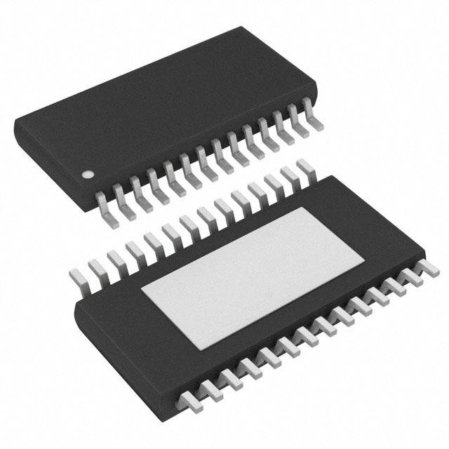
Available in TSSOP28-Exposed Package
APPLICATIONS
•
•
•
•
•
•
Portable Docking Stations
Surround Sound DVD Systems
Televisions
Flat Panel Monitors
Multimedia Computers
Home Stereo Systems
For MPS green status, please visit MPS website under Quality Assurance.
“MPS” and “The Future of Analog IC Technology” are Registered Trademarks of
Monolithic Power Systems, Inc.
AAM (Analog Adaptive Modulation) is a Trademark of Monolithic Power
Systems, Inc.
TYPICAL APPLICATION
THD+N vs. POUT
VDD=24V, Freq=1kHz
20
10
5
2
1
0.5
0.2
0.1
0.05
0.02
0.01
60m 100m
MP7748 Rev. 1.0
1/28/2011
1
POUT (W)
www.MonolithicPower.com
MPS Proprietary Information. Patent Protected. Unauthorized Photocopy and Duplication Prohibited.
© 2011 MPS. All Rights Reserved.
10
35
1
�MP7748 – 2X20W STEREO SINGLE ENDED CLASS D AUDIO AMPLIFIER
ORDERING INFORMATION
Part Number*
MP7748DF
Package
TSSOP28F
Top Marking
Free Air Temperature (TA)
MP7748DF
-40°C to +85°C
* For Tape & Reel, add suffix –Z (e.g. MP7748DF–Z).
For RoHS compliant packaging, add suffix –LF (e.g. MP7748DF–LF–Z)
PACKAGE REFERENCE
TOP VIEW
N/C 1
28 PGND1
REF1 2
27 PGND1
IN1 3
26 SW1
TIMER1 4
25 SW1
AGND1 5
24 BST1
EN1 6
23 VDD1
UVP1 7
IN2 8
EXPOSED PAD
ON BACKSIDE
REF2 9
22 VDD1
21 PGND2
20 PGND2
TIMER2 10
19 SW2
AGND2 11
18 SW2
EN2 12
17 BST2
UVP2 13
16 VDD2
N/C 14
15 VDD2
ABSOLUTE MAXIMUM RATINGS (1)
Thermal Resistance
Supply Voltage VDD ...................................... 40V
BS Voltage ..................VSW – 0.3V to VSW + 6.5V
Enable Voltage VEN .........................-0.3V to +6V
VUVP, VSW, VPIN, VNIN ................... -1V to VDD + 1V
AGND to PGND ...........................-0.3V to +0.3V
Continuous Power Dissipation (TA = +25°C) (2)
………………………………………………....3.9W
Junction Temperature ...............................150°C
Lead Temperature ....................................260°C
Storage Temperature ............... -65°C to +150°C
TSSOP28F .............................. 32 ....... 6 ........ °C
Recommended Operating Conditions
(3)
Supply Voltage VDD .......................... 9.5V to 36V
Maximum Junction Temp. (TJ) ............... +125°C
MP7748 Rev. 1.0
1/28/2011
(4)
θJA
θJC
Notes:
1) Exceeding these ratings may damage the device.
2) The maximum allowable power dissipation is a function of
the maximum junction temperature TJ (MAX), the junction-toambient thermal resistance θJA, and the ambient temperature
TA. The maximum allowable continuous power dissipation at
any ambient temperature is calculated by PD (MAX) =
(TJ(MAX)-TA)/ θJA. Exceeding the maximum allowable power
dissipation will cause excessive die temperature, and the
regulator will go into thermal shutdown. Internal thermal
shutdown circuitry protects the device from permanent
damage.
3) The device is not guaranteed to function outside of its
operating conditions.
4)
Measured on JESD51-7, 4-layer PCB.
www.MonolithicPower.com
MPS Proprietary Information. Patent Protected. Unauthorized Photocopy and Duplication Prohibited.
© 2011 MPS. All Rights Reserved.
2
�MP7748 – 2X20W STEREO SINGLE ENDED CLASS D AUDIO AMPLIFIER
ELECTRICAL CHARACTERISTICS (5, 6)
VDD = 24V, VEN = 5V, TA = +25°C, unless otherwise noted.
Parameters
Symbol Condition
Supply Current
Standby Current
Quiescent Current
Output Drivers
SW On Resistance
Short Circuit Current
Inputs
IQ
EN Enable Threshold Voltage
EN Enable Input Current
External
Undervoltage
Detection
External
Undervoltage
Detection Hysteresis Voltage
Thermal Shutdown
Thermal Shutdown Trip Point
Min
Typ
VEN = 0V,NIN=PIN=Float
SW=Low
140
3
Sourcing and Sinking
Sourcing and Sinking
0.25
4.5
VEN Rising
VEN Falling
VEN = 5V
1.4
1.0
5
0.4
Max
Units
6
µA
mA
Ω
A
2.0
V
V
µA
VUVP
4
V
VHys
0.3
V
150
°C
30
°C
TJ Rising
Thermal Shutdown Hysteresis
Note:
5) The device is not guaranteed to function outside its operating rating.
6) Electrical Characteristics are for the IC only with no external components except bypass capacitors.
MP7748 Rev. 1.0
1/28/2011
www.MonolithicPower.com
MPS Proprietary Information. Patent Protected. Unauthorized Photocopy and Duplication Prohibited.
© 2011 MPS. All Rights Reserved.
3
�MP7748 – 2X20W STEREO SINGLE ENDED CLASS D AUDIO AMPLIFIER
OPERATING SPECIFICATIONS
Circuit of figure 5, single-ended output configuration, VDD = 24V, Gain=8.25V/V, VEN = 5V, TA =
+25°C, unless otherwise noted.
Parameters
Standby Current
Quiescent Current
Power Output
THD+ Noise
Efficiency
Maximum Power Bandwidth
Dynamic Range
Noise Floor
Power Supply Rejection
Symbol Condition
VEN = 0V
Switching, no load
f = 1kHz, THD+N = 10%, 4Ω Load
f = 1kHz, THD+N = 10%, 8Ω Load
POUT = 1W, f = 1kHz, 4Ω Load
POUT = 1W, f = 1kHz, 8Ω Load
f = 1kHz, POUT = 19.3W, 4Ω Load
f = 1kHz, POUT = 10.6W, 8Ω Load
A-Weighted
VCC=24V,
Gain=8.25V/V,
VRIPPLE=200mVPP
CR=100µF
Min
Typ
180
26
19.3
10.6
0.02
0.02
91
96
20
97
103
Max
Units
µA
mA
W
W
%
%
%
%
kHz
dB
µV
f = 1kHz
-59
dB
f = 217Hz
-59
dB
Circuit of figure 6, bridge-tied-load output configuration, VDD = 24V, Gain=15V/V, VEN = 5V, TA =
+25°C, unless otherwise noted.
Parameters
Symbol Condition
Standby Current
Quiescent Current
Power Output
THD+ Noise
Efficiency
Maximum Power Bandwidth
Dynamic Range
Noise Floor
Power Supply Rejection
MP7748 Rev. 1.0
1/28/2011
Min
VEN = 0V
Switching, no load
f = 1kHz, THD+N = 10%, 6Ω Load
f = 1kHz, THD+N = 10%, 8Ω Load
POUT = 1W, f = 1kHz, 6Ω Load
POUT = 1W, f = 1kHz, 8Ω Load
f = 1kHz, POUT = 50W, 6Ω Load
f = 1kHz, POUT = 40W, 8Ω Load
Max
Units
180
26
50
40
0.04
0.03
91
94
20
107
140
µA
mA
W
W
%
%
%
%
kHz
dB
µV
f = 1kHz
-60
dB
f = 217Hz
-60
dB
A-Weighted
VCC=24V,
Gain=15V/V,
VRIPPLE=200mVPP
Typ
www.MonolithicPower.com
MPS Proprietary Information. Patent Protected. Unauthorized Photocopy and Duplication Prohibited.
© 2011 MPS. All Rights Reserved.
4
�MP7748 – 2X20W STEREO SINGLE ENDED CLASS D AUDIO AMPLIFIER
PIN FUNCTIONS
Pin #
Name
1, 14
N/C
2
REF1
3
IN1
4
TIMER1
5
AGND1
6
EN1
7
UVP1
8
IN2
9
REF2
10
TIMER2
11
AGND2
12
EN2
13
UVP2
Under-voltage protection reference input for Amplifier 2. Connect UVP2 to UVP1.
15, 16
VDD2
Power supply input for Amplifier 2. Bypass VDD2 to PGND2 with a 1µF X7R capacitor (in
addition to the main bulk capacitor), placed close to the VDD2 and PGND2 pins.
17
BST2
High-side MOSFET bootstrap input for Amplifier 2. A capacitor from BST2 to SW2
supplies the gate drive current to the internal high-side MOSFET.
18, 19
SW2
Switched power output for Amplifier 2.
20, 21
PGND2
Power ground for Amplifier 2. Connect PGND2 to PGND1. Connect PGND to AGND at a
single point.
22, 23
VDD1
Power supply input for Amplifier 1. Bypass VDD1 to PGND1 with a 1µF X7R capacitor (in
addition to the main bulk capacitor), placed close to the VDD1 and PGND1 pins.
24
BST1
High-side MOSFET bootstrap input for Amplifier 1. A capacitor from BST1 to SW1
supplies the gate drive current to the internal high-side MOSFET.
25, 26
SW1
Switched power output for Amplifier 1.
27, 28
PGND1
Power ground for Amplifier 1. Connect PGND1 to PGND2. Connect PGND to AGND at a
single point.
Exposed
Pad
Connect exposed pad to GND plane for proper thermal performance.
MP7748 Rev. 1.0
1/28/2011
Description
Not connected internally
Internal analog reference (VDD/2) for Amplifier 1. For SE configuration, connect a bypass
capacitor from REF1 to AGND (10µF).
Inverting input for amplifier 1.
Internal timer input for Amplifier 1. Connect a capacitor from TIMER1 to AGND (2.2µF) to
set the internal timer for startup pop elimination.
Analog ground for Amplifier 1. Connect AGND1 to AGND2. Connect PGND to AGND at a
single point.
Enable input for Amplifier 1. Drive EN1 high to turn on the Amplifier 1, low to turn it off.
Under-voltage protection reference input for Amplifier 1. Connect UVP1 to UVP2.
Inverting input for amplifier 2.
Internal analog reference (VDD/2) for Amplifier 2. For SE configuration, connect a bypass
capacitor from REF2 to AGND (10µF).
Internal timer input for Amplifier 2. Connect a capacitor from TIMER2 to AGND (2.2uF) to
set the internal timer for startup pop elimination.
Analog ground for Amplifier 2. Connect AGND2 to AGND1. Connect PGND to AGND at a
single point.
Enable input for Amplifier 2. Drive EN2 high to turn on the Amplifier 2, low to turn it off.
www.MonolithicPower.com
MPS Proprietary Information. Patent Protected. Unauthorized Photocopy and Duplication Prohibited.
© 2011 MPS. All Rights Reserved.
5
�MP7748 – 2X20W STEREO SINGLE ENDED CLASS D AUDIO AMPLIFIER
TYPICAL PERFORMANCE CURVES
Circuit of Figure 5, single-ended output configuration, VDD=24V, VEN=5V, AV=8.25V/V, TA = +25°C,
unless otherwise noted.
20
10
5
20
10
20
10
5
5
2
1
0.5
2
1
2
1
0.2
0.5
0.5
Freq=10kHz
0.1
0.05
0.2
0.1
0.05
Freq=1kHz
0.02
0.01
60m 200m
POUT (W)
0.2
0.1
0.01
+20
+18
+20
+18
+16
+16
+14
+14
+12
+10
+8
10k 20k
+4
+2
+2
-10
+0
-10
-20
-20
AMPLITUDE (dB)
AMPLITUDE (dB)
1k
10k
-30
-40
-50
-60
FREQUENCY (Hz)
MP7748 Rev. 1.0
1/28/2011
100
10k 20k
10k
40k
+0
-20
-30
-40
-50
-60
-80
20
1k
FREQUENCY (Hz)
-70
-70
1k
+0
10
40k
FREQUENCY (Hz)
+0
100
+8
+6
100
10k 20k
+10
+4
+0
10
1k
+12
+6
FREQUENCY (Hz)
-80
20
100
FREQUENCY (Hz)
AMPLITUDE (dBV)
1k
1
GAIN (dB)
GAIN (dB)
1
100
0.02
0.01
20
Freq=100Hz
10
35
POUT (W)
20
10
0.001
20
0.2
0.1
0.05
Freq=1kHz
0.02
0.01
60m 200m
Freq=100Hz
10
35
1
Freq=10kHz
-40
-60
-80
-100
-120
100
1k
FREQUENCY (Hz)
10k 20k
2
4
6 8 10 12 14 16 18 20
FREQUENCY (kHz)
www.MonolithicPower.com
MPS Proprietary Information. Patent Protected. Unauthorized Photocopy and Duplication Prohibited.
© 2011 MPS. All Rights Reserved.
6
�MP7748 – 2X20W STEREO SINGLE ENDED CLASS D AUDIO AMPLIFIER
TYPICAL PERFORMANCE CURVES (continued)
+0
-20
-20
-40
-60
-80
-100
-20
-40
-60
Left to Right
-80
Right to Left
-100
-120
2
4
-120
20
6 8 10 12 14 16 18 20
+0
TT
AMPLITUDE (dB)
+0
AMPLITUDE (dB)
AMPLITUDE (dBV)
Circuit of Figure 5, single-ended output configuration, VDD=24V, VEN=5V, AV=8.25V/V, TA = +25°C,
unless otherwise noted.
-40
-60
Left to Right
-80
Right to Left
-100
100
FREQUENCY (kHz)
1k
-120
20
10k 20k
FREQUENCY (Hz)
100
1k
10k 20k
FREQUENCY (Hz)
POUT vs. VDD
+0
+0
-20
-20
-40
-60
-80
-100
35
30
25
-40
POUT (W)
AMPLITUDE (dBV)
AMPLITUDE (dBV)
Input Signal Frequency =1kHz
the same POUT for both channels
-60
-80
20
1k
100
10k 30k
FREQUENCY (Hz)
60 100
15
10
-100
5
-120
-120
20
1k
10k 30k
FREQUENCY (Hz)
0
0
10
20
30
40
VDD (V)
Note: Dashed Lines represent
thermally limited regions.
Efficiency vs. POUT
VDD = 24V,
Input Signal Frequency=1kHz
100
90
80
70
60
50
40
30
20
10
00
2
4 6
8 10 12 14 16 18 20
P OUT (W)
MP7748 Rev. 1.0
1/28/2011
www.MonolithicPower.com
MPS Proprietary Information. Patent Protected. Unauthorized Photocopy and Duplication Prohibited.
© 2011 MPS. All Rights Reserved.
7
�MP7748 – 2X20W STEREO SINGLE ENDED CLASS D AUDIO AMPLIFIER
TYPICAL PERFORMANCE CURVES (continued)
Circuit of Figure 6, BTL output configuration, VDD=24V, VEN=5V, AV=15V/V, TA = +25°C, unless
otherwise noted.
20
10
5
2
1
0.5
20
10
20
10
5
1
2
1
Freq=10kHz
Freq=10kHz
0.5
0.2
0.1
0.05
0.1
0.2
0.1
Freq=1kHz
Freq=1kHz
0.01
0.05
0.02
Freq=100kHz
0.01
50m 200m
1
10 20
0.02
0.01 Freq=100kHz
50m 200m
1
60
POUT (W)
10 20 50
0.001
20
100
POUT (W)
GAIN (dB)
1
0.1
10k 20k
FREQUENCY (Hz)
+30
+30
+25
+25
+20
+20
GAIN (dB)
20
10
1k
+15
+10
+15
+10
0.01
+5
+5
0.001
20
100
1k
+0
10
10k 20k
1k
10k
+0
10
40k
+0
+0
-10
-20
-20
-20
-40
-50
-60
-30
-40
-50
-60
-70
-70
-80
20
-80
20
1k
FREQUENCY (Hz)
MP7748 Rev. 1.0
1/28/2011
10k 20k
AMPLITUDE (dBV)
+0
-30
1k
10k
40k
FREQUENCY (Hz)
-10
100
100
FREQUENCY (Hz)
AMPLITUDE (dB)
AMPLITUDE (dB)
FREQUENCY (Hz)
100
-40
-60
-80
-100
-120
100
1k
FREQUENCY (Hz)
10k 20k
2
4
6 8 10 12 14 16 18 20
FREQUENCY (kHz)
www.MonolithicPower.com
MPS Proprietary Information. Patent Protected. Unauthorized Photocopy and Duplication Prohibited.
© 2011 MPS. All Rights Reserved.
8
�MP7748 – 2X20W STEREO SINGLE ENDED CLASS D AUDIO AMPLIFIER
TYPICAL PERFORMANCE CURVES (continued)
Circuit of Figure 6, BTL output configuration, VDD=24V, VEN=5V, AV=15V/V, TA = +25°C, unless
otherwise noted.
+0
-40
-60
-80
-100
-120
+0
+0
-20
-20
-40
-60
-80
-100
4
50 100
6 8 10 12 14 16 18 20
FREQUENCY (kHz)
90
70
80
EFFICIENCY(%)
100
80
POUT (W)
40
30
20
10
-80
-100
10k
30k
50 100
1k
10k
30k
FREQUENCY (Hz)
VDD = 24V,
Input Signal Frequency=1kHz
90
50
-60
Efficiency vs. POUT
Input Signal Frequency =1kHz
60
1k
FREQUENCY (Hz)
POUT vs. VDD
-40
-120
-120
2
0
AMPLITUDE (dBV)
AMPLITUDE (dBV)
AMPLITUDE (dBV)
-20
70
60
50
40
30
20
10
0
10
20
30
40
VDD (V)
Note: Dashed Lines represent
thermally limited regions.
MP7748 Rev. 1.0
1/28/2011
0
0 5 10 15 20 25 30 35 40 45 50 55
P OUT (W)
Note: Dashed Line represents
with external heat-sink
www.MonolithicPower.com
MPS Proprietary Information. Patent Protected. Unauthorized Photocopy and Duplication Prohibited.
© 2011 MPS. All Rights Reserved.
9
�MP7748 – 2X20W STEREO SINGLE ENDED CLASS D AUDIO AMPLIFIER
BLOCK DIAGRAM
VDD
REF1
IN1
TIMER1
UVP1
VDD1
Reference
AAMTM Modulator
BST1
SW1
Control&
Gate Drive
OTP
OCP
External
Under Voltage
Detector
PGND1
Shutdown
EN1
EN2
AGND1
VDD
REF2
IN2
Reference
AAMTM Modulator
BST2
VDD2
Control &
Gate Drive
SW2
TIMER2
UVP2
External
Under Voltage
Detector
OTP
OCP
PGND2
AGND2
Figure1—Function block Diagram
MP7748 Rev. 1.0
1/28/2011
www.MonolithicPower.com
MPS Proprietary Information. Patent Protected. Unauthorized Photocopy and Duplication Prohibited.
© 2011 MPS. All Rights Reserved.
10
�MP7748 – 2X20W STEREO SINGLE ENDED CLASS D AUDIO AMPLIFIER
OPERATION
The MP7748 is a Class D Audio Amplifier for
driving stereo speakers in single-ended
configuration or a mono speaker in bridge-tiedload configuration. It uses the Monolithic Power
Systems
patented
Analog
Adaptive
ModulationTM to convert the audio input signal
into pulses. These pulses drive an internal highcurrent output stage and, when filtered through
an external inductor-capacitor filter, reproduce
the input signal across the load. Because of the
switching Class D output stage, power
dissipation in the amplifier is drastically reduced
when compared to Class A, B or A/B amplifiers
while maintaining high fidelity and low
distortion.
REF1/2 are the positive inputs of the two
amplifiers. They are set to half the DC power
supply input voltage (VDD/2) by the internal
circuit. The input capacitor CIN couple the AC
signal at the input.
The amplifier voltage gain is set by the
combination of the input resister RIN1/2 and the
feedback resistor RFB1/2 and is calculated by the
equation:
AV =
−R FB
R IN
The MP7748 includes four high-power
MOSFETs wherein for each channel the output
driver stage uses two 250mΩ N-channel
MOSFETs to deliver the pulses to the LC output
filter which in turn drives the load. To fully
enhance the high-side MOSFET, the gate is
driven to a voltage higher than the source by
the bootstrap capacitor between SW and BS.
While the output is driven low, the bootstrap
capacitor is charged from VDD through an
internal circuit on the MP7748. The gate of the
high-side MOSFET is driven high from the
voltage at BS, forcing the MOSFET gate to a
voltage higher than VDD and allowing the
MOSFET to fully turn on, reducing power loss in
the amplifier.
Pop Elimination
The MP7748 integrates a source current
function to charge the AC coupling capacitor
COUT1/2 for the SE output configuration and CIN1/2
at the start up moment. The start up source
current slew rate is adjustable by selecting
MP7748 Rev. 1.0
1/28/2011
different capacitance of timer capacitor
CTIMER1/2. The larger the capacitance of the timer
capacitor is, the smaller the start up current
slew rate is. The recommended 2.2µF timer
capacitor results in a start up current slew rate
of approximately 20mA/350ms which would
help to minimize the turn on pop.
After driving EN pin low, output SW will be set
to high impedance immediately which would
help to eliminate the turn off pop.
Short Circuit/Overload Protection
The MP7748 has internal overload and short
circuit protection. The currents in both the highside and low-side MOSFETs are measured and
if the current exceeds the 4.5A short circuit
current limit, both MOSFETs are turned off. The
MP7748 then restarts with the same power up
sequence that is used for normal starting to
prevent a pop from occurring after a short
circuit condition is removed.
Enable Function
The MP7748 EN input is an active high enable
control. To enable the MP7748, drive EN with a
2.0V or higher voltage. To disable the amplifier,
drive it below 0.4V. While the MP7748 is
disabled, the VDD operating current is less than
140µA and the output driver MOSFETs are
turned off.
Programmable UVP
MP7748 integrate programmable UVP function,
which can be used to shutdown the MP7748 to
escape the pop, by controlling the UVP node
voltage. The corresponding circuit is shown in
the followed figure 2. If the UVP pin is NC, the
default VDD shutdown voltage (rising threshold)
is 8.4V since there is internal voltage divided
circuit. The VDD shutdown voltage can be
flexibly adjusted by controlling UVP pin voltage
The recommended VDD shutdown voltage is
from 9.5V to power supply. As shown in the
figure 2, if external resistor RH and RL is low
enough (e.g. RH, RL < 50kΩ) compared with
internal 500kΩ and 550kΩ resistor, the VDD
shutdown voltage (rising threshold) can be
calculated by the equation:
www.MonolithicPower.com
MPS Proprietary Information. Patent Protected. Unauthorized Photocopy and Duplication Prohibited.
© 2011 MPS. All Rights Reserved.
11
�MP7748 – 2X20W STEREO SINGLE ENDED CLASS D AUDIO AMPLIFIER
VVDD _ shutdown = 4 *
(RH + RL )
RL
The hysteresis voltage can be calculated by the
equation:
Vhysteresis = 10% * VVDD _ shutdown
Figure 2—UVP block diagram
MP7748 Rev. 1.0
1/28/2011
www.MonolithicPower.com
MPS Proprietary Information. Patent Protected. Unauthorized Photocopy and Duplication Prohibited.
© 2011 MPS. All Rights Reserved.
12
�MP7748 – 2X20W STEREO SINGLE ENDED CLASS D AUDIO AMPLIFIER
APPLICATION INFORMATION
Component Selection
The MP7748 uses a minimum number of external
components to complete a stereo SE or mono
BTL Class D audio amplifier. The circuit of Figure
3 (stereo SE application circuit) and figure 4
(mono BLT application circuit) are optimized for a
24V power supply. This circuit should be suitable
for most applications, and use the following
sections to determine how to customize the
amplifier for a particular application.
with 50k Hz difference by using different timing
capacitor CINT. For detailed please refer to the
table 1 for recommended SE output configuration
design, and table 2 for recommended BTL output
configuration design.
Table 1—Switching Frequency Setting For SE
Output Configuration
VDD Gain RFB RIN
(V) (V/V) (kΩ) (kΩ)
Setting the Voltage Gain
The maximum output voltage swing is limited by
the power supply. To achieve the maximum
power out of the MP7748 amplifier, set the gain
such that the maximum input signal results in the
maximum output voltage swing.
For single-ended (SE) output configuration, the
maximum output voltage VOUT(PK) is VDD/2. For
bridge-tied-load (BTL) output configuration, the
maximum output voltage VOUT(PK) is VDD. For a
given input signal voltage, where VIN(PK) is the
peak input voltage, the maximum voltage gain is:
A V (MAX) =
12
5.6
56
10
4.7
560
3.3
700
12
8.2
39
4.7
5.6
620
4.7
700
12
12.0 56.4
4.7
4.7
530
3.3
670
12
17.6 56.4
3.2
4.7
530
3.3
670
12
25.5 56.4
2.2
4.7
530
3.3
670
12
30
60
2
4.7
520
3.3
650
24
5.6
56
10
10
540
8.2
650
24
8.2
82
10
5.6
610
4.7
690
24
12.0
120
10
4.7
530
3.3
660
24
17.4
82
4.7
5.6
610
4.7
690
VOUT ( PK )
24
25.5
120
4.7
4.7
530
3.3
660
VIN ( PK )
24
30
120
4
4.7
530
3.3
660
This voltage gain setting results in the peak
output voltage approaching it’s maximum for the
maximum input signal. In some cases the
amplifier is allowed to overdrive slightly, allowing
the THD to increase at high power levels, and so
a higher gain than AV (max) is required.
Setting the Switching Frequency
The idle switching frequency (the switching
frequency when no audio input is present) is a
function of several variables: the supply voltage
VDD, the integral capacitor CINT and the feedback
resistor RFB. Lower switching frequency results in
more inductor ripple, causing more quiescent
output voltage ripple and increasing the output
noise
and
distortion.
Higher
switching
frequencies result in more power loss. The
optimum quiescent switching frequency is
approximately 600kHz. When used to drive
stereo speakers in single-ended configuration, it
is recommended to set right channel idle
switching frequency larger than left channel’s
MP7748 Rev. 1.0
1/28/2011
Left
Right
channel
channel
CINT1 FSW1 CINT2 FSW2
(nF) (kHz) (nF) (kHz)
Table 2 - Switching Frequency Setting For
BTL Output Configuration
VDD Gain RFB RIN
(V) (V/V) (kΩ) (kΩ)
CINT1 FSW1
(nF) (kHz)
12
10
100
10
3.9
400
12
20
100
5
3.3
400
12
30
121
4.02
2.7
400
24
10
100
10
3.9
580
24
20
121
6.04
3.9
480
24
30
121
4.02
3.9
480
32
10
100
10
4.7
580
32
20
121
6.04
3.9
560
32
30
162
5.36
3.3
500
www.MonolithicPower.com
MPS Proprietary Information. Patent Protected. Unauthorized Photocopy and Duplication Prohibited.
© 2011 MPS. All Rights Reserved.
13
�MP7748 – 2X20W STEREO SINGLE ENDED CLASS D AUDIO AMPLIFIER
Choosing the Output LC Filter
The Inductor-Capacitor (LC) filter converts the
pulse train at SW to the output voltage that drives
the speaker. There are two kinds of LC filter
structure depending on the output configuration.
COUT
LF
SW1/2
CF
RLOAD
Figure 3—SE Filter Configuration
LF1
SW1
CY1
CY2
SW2
CX
RLOAD
LF2
Figure 4—BTL Filter Configuration
Where:
L F = L F1 + L F 2 ,
CF = CX +
C Y1 × C Y 2
,
C Y1 + C Y 2
L F1 = L F 2 ;
C Y1 = C Y 2
The characteristic frequency of the LC filter
needs to be high enough to allow high frequency
audio to the output, yet needs to be low enough
to filter out high frequency products of the pulses
from SW. The characteristic frequency of the LC
filter is:
f0 =
1
2 × π × L F × CF
The quality factor (Q) of the LC filter is important.
If this is too low, output noise will increase, if this is
too high, then peaking may occur at high signal
frequencies reducing the passband flatness. The
circuit Q is set by the load resistance (speaker
resistance, typically 4Ω or 8Ω). The Q is
calculated as:
Q=
MP7748 Rev. 1.0
1/28/2011
RLOAD
RLOAD
=
ω0 × LF 2π × f0 × LF
ω0 is the characteristic frequency in radians per
second and f0 is in Hz. Use an LC filter with Q
between 0.7 and 1.
The actual output ripple and noise is greatly
affected by the type of inductor and capacitor used
in the LC filter. Use a film capacitor and an
inductor with sufficient power handling capability
to supply the output current to the load. The
inductor
should
exhibit
soft
saturation
characteristics. If the inductor exhibits hard
saturation, it should operate well below the
saturation current. Gapped ferrite, MPP,
Powdered Iron, or similar type toroidal cores are
recommended. If open or shielded bobbin ferrite
cores are used for multi-channel designs, make
sure that the start windings of each inductor line
up (all starts going toward SW pin, or all starts
going toward the output) to prevent crosstalk or
other channel-to-channel interference.
Output Coupling Capacitor For SE Output
The output AC coupling capacitor COUT serves to
block DC voltages and thus passes only the
amplified AC signal from the LC filter to the load.
The combination of the coupling capacitor, COUT
and the load resistance results in a first-order
high-pass filter. The value of COUT should be
selected such that the required minimum
frequency is still allowed to pass. The output
corner frequency (-3dB point), fOUT, can be
calculated as:
f OUT =
1
2 × π × R LOAD × C OUT
Set the output corner frequency (fOUT) at or below
the minimum required frequency.
The output coupling capacitor carries the full load
current, so a capacitor should be chosen such
that its ripple current rating is greater than the
maximum load current. Low ESR aluminum
electrolytic capacitors are recommended.
Input Coupling Capacitor
The input coupling capacitors CIN1 and CIN2 are
used to pass only the AC signal at the input. In a
typical system application, the source input signal
is typically centered around the circuit ground,
while the MP7748 input is at half the power
supply voltage (VDD/2). The input coupling
capacitor transmits the AC signal from the source
www.MonolithicPower.com
MPS Proprietary Information. Patent Protected. Unauthorized Photocopy and Duplication Prohibited.
© 2011 MPS. All Rights Reserved.
14
�MP7748 – 2X20W STEREO SINGLE ENDED CLASS D AUDIO AMPLIFIER
to the MP7748 while blocking the DC voltage.
Choose an input coupling capacitor such that the
corner frequency (fIN) is less than the passband
frequency. The corner frequency is calculated as:
fIN =
1
2 × π × R IN × CIN
Timer capacitor
The start up source current slew rate is
adjustable by selecting different capacitance of
timer capacitor CTIMER. The larger the CTIMER
capacitance is, the smaller the start up current
slew rate is. It is recommended to use the CTIMER
which capacitance is larger than 312nF, so the
start up current slew rate would be smaller than
20mA/50ms which would help to eliminate the
turn on pop. The recommended 2.2µF capacitor
CTIMER results in a start up current slew rate of
approximately 20mA/350ms.
Power Source
For maximum output power, the amplifier circuit
requires a regulated external power source to
supply the power to the amplifier. The higher the
power supply voltage, the more power can be
delivered to a given load resistance, however if
the power source voltage exceeds the maximum
voltage of 36V, the MP7748 may sustain
damage. The power supply rejection of the
MP7748 is excellent, however noise at the power
supply can get to the output, so care must be
taken to minimize power supply noise within the
pass-band frequencies. Bypass the power supply
with a large capacitor (typically aluminum
electrolytic) along with a smaller 1µF ceramic
capacitor at the MP7748 VDD supply pins.
possible. Likewise, place CBS2 as close to BST2
pin and SW2 pins as possible.
Power Supply Bypass Cap
CBYP1 and CBYP2 carry the transient current for the
switching power stage. To prevent overstressing
of the MP7748 and excessive noise at the output,
place CBYP1 as close to VDD1 pins and PGND1
pins as possible and also place CBYP2 as close to
VDD2 pins and PGND2 pins as possible.
Integral Capacitors
CINT are used to set the amplifier switching
frequencies and are typically on the order of a
few nF. Place the integral capacitor CINT as close
to the corresponding input as possible to reduce
distortion and noise. For example, place CINT1 as
close to pins 2 and 3 as possible at SE output
configuration.
Reference Bypass Capacitors For SE Output
When used with SE output, CR1 and CR2 is
needed to filter the ½ VDD reference voltages.
Place CR1 and CR2 as close to the IC as possible
to improve power supply rejection and reduce
distortion and noise at the output.
2) The Inductor-Capacitor (LC) filter converts the
pulse train at SW to the output voltage that drives
the speaker. Please keep the filter capacitor
close to the inductor.
Bootstrap Cap
3) When laying out the PCB, use two separate
ground planes, analog ground (AGND) and
power ground (PGND), and connect the two
grounds together at a single point (usually
around the bulk bypass capacitor) to prevent
noise injection into the amplifier input to reduce
distortion.
4) Keep the sensitive feedback signal trace on
the input side and shield the trace with the AGND
plane. Make sure that any traces carrying the
switch node (SW) voltages are separated far
from any input signal traces. If it is required to run
the SW trace near the input, shield the input with
a ground plane between the traces. Make sure
that each channel is physically separated to
prevent crosstalk. Make sure that all inductors
used on a single circuit board have the same
orientation.
CBS1 and CBS2 are used to supply the gate drive
current to the internal high-side MOSFET. Place
CBS1 as close to BST1/2 pin and SW1/2 pin as
Also, make sure that the power supply is routed
from the source to each channel individually, not
serially. This prevents channel-to-channel
PCB Layout
The circuit layout is critical for optimum
performance and low output distortion and noise.
It is highly recommended to duplicate EVB layout
for optimum performance. If change is
necessary, please follow these guidelines and
take Figure 7 for references.
1) Place the following components as close to
the MP7748 as possible:
MP7748 Rev. 1.0
1/28/2011
www.MonolithicPower.com
MPS Proprietary Information. Patent Protected. Unauthorized Photocopy and Duplication Prohibited.
© 2011 MPS. All Rights Reserved.
15
�MP7748 – 2X20W STEREO SINGLE ENDED CLASS D AUDIO AMPLIFIER
coupling through the power supply input.
Electro-Magnetic
Considerations
Interference
(EMI)
Due to the switching nature of the Class D
amplifier, care must be taken to minimize the
effects of electromagnetic interference from the
amplifier. However, with proper component
selection and careful attention to circuit layout,
the effects of the EMI due to the amplifier
switching can be minimized.
The power inductors are a potential source of
radiated emissions. For the best EMI
performance, use toroidal inductors, since the
magnetic field is well contained inside the core.
However toroidal inductors can be expensive to
wind. For a more economical solution, use
shielded gapped ferrite or shielded ferrite bobbin
core inductors. These inductors typically do not
contain the field as well toroidal inductors, but
usually can achieve a better balance of good EMI
performance with low cost.
The size of high-current loops that carry rapidly
changing currents needs to be minimized. To do
this, make sure that the VDD bypass capacitors
are as close to the MP7748 as possible.
Nodes that carry rapidly changing voltage, such
as SW, need to be made as small as possible. If
sensitive traces run near a trace connected to
SW, place a ground shield between the traces.
MP7748 Rev. 1.0
1/28/2011
www.MonolithicPower.com
MPS Proprietary Information. Patent Protected. Unauthorized Photocopy and Duplication Prohibited.
© 2011 MPS. All Rights Reserved.
16
�MP7748 – 2X20W STEREO SINGLE ENDED CLASS D AUDIO AMPLIFIER
YPICAL APPLICATION CIRCUIT
CFB1
RFB1
CIN1
2
CR1
REF1
CINT1
RIN1
CH1
INPUT
3
4
BST1
24
IN1
C
TIMER1
SW1
25,26
10
CF1
TIMER2
MP7748
CIN2
9 REF2
CR2
6
SW2
IN2
VDD1
EN1
PGND1
12 EN2
5
AGND1
EN
LF2
1uF
8
CH2
INPUT
17
CBS2
CINT2
RIN2
BST2
VDD2
11 AGND2
7 UVP1
13 UVP2
PGND2
CH1
OUTPUT
COUT2
18,19
22,23
CF2
VDD
CBYP1
27,28
CVDDBYP
1000
CH2
OUTPUT
15,16
CBYP2
20,21
RFB2
CFB2
Figure 5—24V VDD Stereo SE Typical Application Circuit
CFB1
27pF
U1
3
2
4
IN1
CINT
1nF
21, 23
BST1
24
REF1
SW1 25, 26
TIMER1
6 EN1
12 EN2
EN
VDD2
SW2
CFBX1
1pF
PGND1
27, 28
MP7748
10
UVP2
8 IN2
CFBX2
1pF
5
SW1
SP-
17
SP+
SW2
TIMER2
9 REF2
INPUT-
BST2
SW2
AGND2
13
VCC
RSN1
10
CSN1
390pF
50V
7 UVP1
AGND1
INPUT+
VDD1
15, 16
VCC
11
PGND2
18, 19
20, 21
RSN2
10
CSN2
390pF
50V
SW1
CFB2
27pF
Figure 6—24V VDD mono BTL Typical Application Circuit
MP7748 Rev. 1.0
1/28/2011
www.MonolithicPower.com
MPS Proprietary Information. Patent Protected. Unauthorized Photocopy and Duplication Prohibited.
© 2011 MPS. All Rights Reserved.
17
�MP7748 – 2X20W STEREO SINGLE ENDED CLASS D AUDIO AMPLIFIER
AGND
PGND
CVDDBYP
CFB1
RFB1
CR1
1
CINT1
CINT2
CR2
NC
PGND1
28
2
REF1
PGND1
27
3
IN1
SW1
26
4
TIMER1
SW1
25
5
AGND1
BST1
24
6
EN1
VDD1
23
7
UVP1
VDD1
22
8
IN2
PGND2
21
9
REF2
PGND2
20
MP7748
10
TIMER2
SW2
19
11
AGND2
SW2
18
12
EN2
BST2
17
13
UVP2
VDD2
16
14
NC
VDD2
15
CF1
LF1
CBS1
CBYP1
LF2
CBS2
CF2
CBYP2
RFB2
Feedback
signal
CFB2
Top
Bottom
Figure 7—Stereo SE Reference PCB Layout
PGND
AGND
PGND
AGND
CFB1
RFB1
CFX1
1
NC
PGND1
28
2
REF1
PGND1
27
3
IN1
SW1
26
4
TIMER1
SW1
25
5
AGND1
BST1
24
6
EN1
VDD1
23
7
UVP1
VDD1
22
8
IN2
PGND2
21
9
REF2
PGND2
20
MP7748
10
TIMER2
SW2
19
11
AGND2
SW2
18
12
EN2
BST2
17
13
UVP2
VDD2
16
14
NC
VDD2
15
LF1
CBS1
CBYP1
LF2
CBS2
CBYP2
CFX2
RFB2
Feedback
signal
CFB2
CVDDBYP
Top
Bottom
Figure 8—Mono BTL Reference PCB Layout
MP7748 Rev. 1.0
1/28/2011
www.MonolithicPower.com
MPS Proprietary Information. Patent Protected. Unauthorized Photocopy and Duplication Prohibited.
© 2011 MPS. All Rights Reserved.
18
�MP7748 – 2X20W STEREO SINGLE ENDED CLASS D AUDIO AMPLIFIER
PACKAGE INFORMATION
TSSOP28
PACKAGE OUTLINE DRAWING FOR 28-TSSOP w/ EXPOSED PADDLE
5.90
TYP
9.60
9.80
0.65
BSC
0.40
TYP
28
15
1.60
TYP
4.30
4.50
PIN 1 ID
3.20
TYP
6.20
6.60
5.80
TYP
14
1
TOP VIEW
RECOMMENDED LAND PATTERN
0.80
1.05
1.20 MAX
SEATING PLANE
0.19
0.30
0.65 BSC
0.00
0.15
0.09
0.20
SEE DETAIL "A"
FRONT VIEW
SIDE VIEW
GAUGE PLANE
0.25 BSC
5.70
6.10
0o-8o
0.45
0.75
DETAIL “A”
2.60
3.10
BOTTOM VIEW
NOTE:
1) ALL DIMENSIONS ARE IN MILLIMETERS.
2) PACKAGE LENGTH DOES NOT INCLUDE MOLD FLASH,
PROTRUSION OR GATE BURR.
3) PACKAGE WIDTH DOES NOT INCLUDE INTERLEAD FLASH
OR PROTRUSION.
4) LEAD COPLANARITY (BOTTOM OF LEADS AFTER FORMING)
SHALL BE 0.10 MILLIMETERS MAX.
5) DRAWING CONFORMS TO JEDEC MO-153, VARIATION AET.
6) DRAWING IS NOT TO SCALE.
NOTICE: The information in this document is subject to change without notice. Please contact MPS for current specifications.
Users should warrant and guarantee that third party Intellectual Property rights are not infringed upon when integrating MPS
products into any application. MPS will not assume any legal responsibility for any said applications.
MP7748 Rev. 1.0
1/28/2011
www.MonolithicPower.com
MPS Proprietary Information. Patent Protected. Unauthorized Photocopy and Duplication Prohibited.
© 2011 MPS. All Rights Reserved.
19
�