MP8758H
High-Current, 10A, 22V, Synchronous
Step-Down Converter with Hiccup OCP, PFM/PWM
The Future of Analog IC Technology Mode Selection, and Auto-Retry Thermal Shutdown
DESCRIPTION
The MP8758H is a fully integrated, highfrequency, synchronous, rectified, step-down
converter. It offers a very compact solution to
achieve a 10A output current with excellent load
and line regulation over a wide input supply
range.
The MP8758H employs a constant-on-time
(COT) control scheme, which provides fast
transient response and eases loop stabilization.
The COT control scheme provides a seamless
transition into PFM mode at light-load operation,
which boosts light-load efficiency.
An open-drain power good signal indicates that
the output voltage is within its nominal voltage
range.
Full protection features include over-current
protection (OCP), over-voltage and under-voltage
protection (OVP, UVP), and thermal shutdown.
FEATURES
•
•
•
•
•
•
•
•
•
•
•
Wide 4.5V to 22V Operating Input Range
10A Continuous Output Current
Low RDS(ON) Internal Power MOSFETs
Proprietary Switching Loss Reduction
Internal Soft Start
Output Discharge
500kHz Switching Frequency
PFM/PWM Mode Selection
Hiccup Mode, OCP, OVP, and UVP
Auto-Retry Thermal Shutdown
Output Adjustable from 0.604V
APPLICATIONS
•
•
•
Set-Top Boxes and Multi-Function Printers
Flat-Panel Televisions and Monitors
Distributed Power Systems
All MPS parts are lead-free, halogen-free, and adhere to the RoHS directive. For
MPS green status, please visit the MPS website under Quality
Assurance. “MPS” and “The Future of Analog IC Technology” are registered
trademarks of Monolithic Power Systems, Inc.
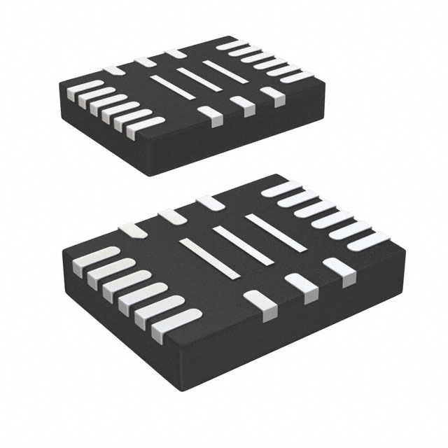
The MP8758H requires a minimal number of
readily available, external components and is
available in a QFN-21 (3mmx4mm) package.
TYPICAL APPLICATION
Efficiency vs.
Output Current
100
90
80
70
60
50
40
VIN=4.5V
VIN=12V
VIN=22V
30
20
10
0.01
MP8758H Rev.1.0
10/13/2015
0.1
1
LOAD CURRENT(A)
www.MonolithicPower.com
MPS Proprietary Information. Patent Protected. Unauthorized Photocopy and Duplication Prohibited.
© 2015 MPS. All Rights Reserved.
10
1
�MP8758H–22V, HIGH-CURRENT SYNCHRONOUS BUCK CONVERTER
ORDERING INFORMATION
Part Number*
Package
Top Marking
MP8758HGL
QFN-21 (3mmx4mm)
See Below
* For Tape & Reel, add suffix –Z (e.g. MP8758HGL–Z)
TOP MARKING
MP: MPS prefix
Y: Year code
W: Week code
8758H: First five digits of the part number
LLL: Lot number
PACKAGE REFERENCE
TOP VIEW
QFN-21 (3mmx4mm)
MP8758H Rev.1.0
10/13/2015
www.MonolithicPower.com
MPS Proprietary Information. Patent Protected. Unauthorized Photocopy and Duplication Prohibited.
© 2015 MPS. All Rights Reserved.
2
�MP8758H–22V, HIGH-CURRENT SYNCHRONOUS BUCK CONVERTER
ABSOLUTE MAXIMUM RATINGS (1)
Supply voltage (VIN) ..................................... 24V
VSW ...............................................-0.3V to 24.3V
VSW (30ns)..........................................-3V to 28V
VSW (5ns)............................................-6V to 28V
VBST ................................................... VSW + 5.5V
VEN ............................................................... 12V
Enable current (IEN) (2)............................... 2.5mA
All other pins ................................-0.3V to +5.5V
(3)
Continuous power dissipation (TA=+25°C)
QFN-21 (3mmx4mm). ................................ 2.5W
Junction temperature ................................150°C
Lead temperature .....................................260°C
Storage temperature ................ -65°C to +150°C
Recommended Operating Conditions
Thermal Resistance
(5)
θJA
θJC
QFN-21 (3mmx4mm) ..............50 ...... 12 ... °C/W
NOTES:
1) Exceeding these ratings may damage the device.
2) For details on EN’s ABS MAX rating, please refer to the “EN
Control section on page 14.
3) The maximum allowable power dissipation is a function of the
maximum junction temperature TJ (MAX), the junction-toambient thermal resistance θJA, and the ambient temperature
TA. The maximum allowable continuous power dissipation at
any ambient temperature is calculated by PD (MAX) =
(TJ(MAX)-TA)/θJA. Exceeding the maximum allowable power
dissipation produces an excessive die temperature, causing
the regulator to go into thermal shutdown. Internal thermal
shutdown circuitry protects the device from permanent
damage.
4) The device is not guaranteed to function outside of its
operating conditions.
5) Measured on JESD51-7, 4-layer PCB.
(4)
Supply voltage (VIN) .........................4.5V to 22V
Output voltage (VOUT)..........................................
0.604V to VINxDMAX or 5.5V
Enable current (IEN) ..................................... 1mA
Operating junction temp. (TJ). .. -40°C to +125°C
MP8758H Rev.1.0
10/13/2015
www.MonolithicPower.com
MPS Proprietary Information. Patent Protected. Unauthorized Photocopy and Duplication Prohibited.
© 2015 MPS. All Rights Reserved.
3
�MP8758H–22V, HIGH-CURRENT SYNCHRONOUS BUCK CONVERTER
ELECTRICAL CHARACTERISTICS
VIN = 12V, TJ = 25°C, unless otherwise noted.
Parameters
Symbol
Supply Current
Supply current (shutdown)
Supply current (quiescent)
ISD
IQ
Condition
VEN = 0V
VEN = 2V, VFB = 0.65V
Min
Typ
Max
Units
160
0
190
1
220
μA
μA
MOSFET
High-side switch-on resistance
HSRDS-ON
TJ = 25°C
25
mΩ
Low-side switch-on resistance
LSRDS-ON
TJ = 25°C
VEN = 0V, VSW = 0V
9
mΩ
Switch leakage
SWLKG
0
1
μA
10
11
12
A
400
250
500
300
600
350
kHz
ns
VOVP_OUT
110
120
TOVPDEL
VUVP
TUVPDEL
55
115
10
2.5
60
12
%VREF
%VREF
μs
%VREF
μs
595
604
10
2.9
613
50
mV
nA
ms
1.15
1.25
100
3
0
1.35
V
mV
VCCVth
4.2
4.35
VCCHYS
400
Current Limit
Low-side valley current limit
ILIMIT
Switching Frequency and Minimum Off Time
Switching frequency
Minimum off time(6)
FSW
TOFF
Output Over-Voltage and Under-Voltage Protection
OVP threshold
OVP hysteresis
OVP delay
UVP threshold
UVP delay
65
Reference and Soft Start
Reference voltage
Feedback current
Soft-start time
VREF
IFB
TSS
VFB = 0.604V
VOUT from 10% to 90%
Enable and UVLO
Enable input low voltage
Enable hysteresis
Enable input current
VCC under-voltage lockout
threshold rising
VCC under-voltage lockout
threshold hysteresis
MP8758H Rev.1.0
10/13/2015
VILEN
VEN-HYS
IEN
VEN = 2V
VEN = 0V
www.MonolithicPower.com
MPS Proprietary Information. Patent Protected. Unauthorized Photocopy and Duplication Prohibited.
© 2015 MPS. All Rights Reserved.
μA
V
mV
4
�MP8758H–22V, HIGH-CURRENT SYNCHRONOUS BUCK CONVERTER
ELECTRICAL CHARACTERISTICS (continued)
VIN = 12V, TJ = 25°C, unless otherwise noted.
Parameters
Symbol
Condition
Min
Typ
Max
Units
4.8
5.1
2
5.3
V
%
VCC Regulator
VCC regulator
VCC load regulation
VCC
Icc = 8mA
Mode Selection
VCC0.4V
Mode high level
Mode low level
Mode internal pull-up resistor
V
0.4V
1
V
MΩ
Power Good
FB rising (good)
PGVth-Hi
95
FB falling (fault)
PGVth-Lo
85
FB rising (fault)
PGVth-Hi
115
FB falling (good)
PGVth-Lo
105
PGTd
800
Power-good low to high delay
Power-good sink-current
capability
Power good leakage current
%VREF
μs
VPG
Sink 4mA
0.4
V
IPG_LEAK
VPG = 3.3V
1
μA
Thermal Protection
Thermal shutdown(6)
Thermal shutdown hysteresis(6)
TSD
150
25
°C
°C
NOTE:
6) Guaranteed by design and engineering sample characterization.
MP8758H Rev.1.0
10/13/2015
www.MonolithicPower.com
MPS Proprietary Information. Patent Protected. Unauthorized Photocopy and Duplication Prohibited.
© 2015 MPS. All Rights Reserved.
5
�MP8758H–22V, HIGH-CURRENT SYNCHRONOUS BUCK CONVERTER
TYPICAL PERFORMANCE CHARACTERISTICS
VIN = 12V, VOUT = 1.2V, L = 1.2µH, TA = +25°C, unless otherwise noted.
100
Efficiency vs. Output
Current
Load Regulation
Line Regulation
2.5
2
90
2
1.5
80
1.5
70
1
VIN=4.5V
60
40
-0.5
-1.5
20
-2
-2.5
10
Enabled Supply Current
vs. Input Voltage
14
400
-1
-1.5
VIN=4.5V
0
1
2 3 4 5 6 7 8 9 10
OUTPUT CURRENT (A)
-2
4
IOUT=10A
6
8 10 12 14 16 18 20 22
INPUT VOLTAGE (V)
Valley Current Limit
vs. Temperature
13
CURRENT LIMIT (A)
350
300
250
200
150
100
50
0
IOUT=5A
0
-0.5
-1
30
0.1
1
OUTPUT CURRENT (A)
0.5
VIN=12V
0
VIN=22V
10
0.01
1
VIN=22V
0.5
VIN=12V
50
IOUT=0A
12
11
10
9
8
7
6
5
0
5
10
15
20
INPUT VOLTAGE (V)
MP8758H Rev.1.0
10/13/2015
25
4
-40 -20
0
20
40
60
80 100
www.MonolithicPower.com
MPS Proprietary Information. Patent Protected. Unauthorized Photocopy and Duplication Prohibited.
© 2015 MPS. All Rights Reserved.
6
�MP8758H–22V, HIGH-CURRENT SYNCHRONOUS BUCK CONVERTER
TYPICAL PERFORMANCE CHARACTERISTICS (continued)
VIN = 12V, VOUT = 1.2V, L = 1.2µH, TA = +25°C, unless otherwise noted.
Start-Up through VIN
Start-Up through VIN
IOUT=0A, PFM
VOUT
500mV/div.
VOUT
500mV/div.
VPG
5V/div.
VIN
10V/div.
VSW
10V/div.
IINDUCTOR
2A/div.
Shutdown through VIN
IINDUCTOR
10A/div.
Shutdown through VIN
IOUT=0A, PFM
IOUT=10A
VOUT
500mV/div.
VPG
5V/div.
VIN
5V/div.
VSW
10V/div.
VIN
5V/div.
VSW
5V/div.
IINDUCTOR
2A/div.
IINDUCTOR
2A/div.
Shutdown through VIN
IOUT=0A, PWM
VOUT
500mV/div.
VOUT
500mV/div.
VPG
5V/div.
VIN
5V/div.
VSW
10V/div.
IOUT=10A
VOUT
500mV/div.
VPG
5V/div.
VIN
10V/div.
VSW
10V/div.
VIN
5V/div.
VSW
5V/div.
IINDUCTOR
2A/div.
Start-Up through VIN
IOUT=0A, PWM
IINDUCTOR
10A/div.
Start-Up through EN
Start-Up through EN
Start-Up through EN
IOUT=0A, PFM
IOUT=0A, PWM
IOUT=10A
VOUT
500mV/div.
VPG
5V/div.
VEN
5V/div.
VSW
10V/div.
IINDUCTOR
2A/div.
MP8758H Rev.1.0
10/13/2015
VOUT
500mV/div.
VEN
5V/div.
VSW
5V/div.
IINDUCTOR
2A/div.
VOUT
500mV/div.
VPG
5V/div.
VEN
5V/div.
VSW
10V/div.
IINDUCTOR
10A/div.
www.MonolithicPower.com
MPS Proprietary Information. Patent Protected. Unauthorized Photocopy and Duplication Prohibited.
© 2015 MPS. All Rights Reserved.
7
�MP8758H–22V, HIGH-CURRENT SYNCHRONOUS BUCK CONVERTER
TYPICAL PERFORMANCE CHARACTERISTICS (continued)
VIN = 12V, VOUT = 1.2V, L = 1.2µH, TA = +25°C, unless otherwise noted.
Shutdown through EN
Shutdown through EN
Shutdown through EN
IOUT=0A, PFM
IOUT=0A, PWM
IOUT=10A
VOUT
500mV/div.
VPG
5V/div.
VEN
5V/div.
VSW
10V/div.
VOUT
500mV/div.
VEN
5V/div.
VOUT
500mV/div.
VPG
5V/div.
VEN
5V/div.
VSW
10V/div.
VSW
5V/div.
IINDUCTOR
2A/div.
IINDUCTOR
10A/div.
IINDUCTOR
10A/div.
Output Voltage Ripple
Output Voltage Ripple
Output Voltage Ripple
IOUT=0A, PFM
IOUT=0A, PWM
IOUT=10A
VOUT/AC
50mV/div.
VOUT/AC
20mV/div.
VOUT/AC
20mV/div.
VIN
5V/div.
VIN
5V/div.
VIN
5V/div.
VSW
5V/div.
VSW
5V/div.
VSW
5V/div.
IINDUCTOR
2A/div.
IINDUCTOR
2A/div.
IINDUCTOR
10A/div.
Load Transient Response
Short-Circuit Entry
Short-Circuit Recovery
IOUT=5A to 10A
IOUT=10A
IOUT=10A
VOUT
50mV/div.
IOUT
5A/div.
MP8758H Rev.1.0
10/13/2015
VOUT
500mV/div.
VOUT
500mV/div.
VIN
10V/div.
VIN
10V/div.
VSW
5V/div.
VSW
5V/div.
IINDUCTOR
10A/div.
IINDUCTOR
10A/div.
www.MonolithicPower.com
MPS Proprietary Information. Patent Protected. Unauthorized Photocopy and Duplication Prohibited.
© 2015 MPS. All Rights Reserved.
8
�MP8758H–22V, HIGH-CURRENT SYNCHRONOUS BUCK CONVERTER
TYPICAL PERFORMANCE CHARACTERISTICS (continued)
VIN = 12V, VOUT = 1.2V, L = 1.2µH, TA = +25°C, unless otherwise noted.
MP8758H Rev.1.0
10/13/2015
Output OVP Entry
Output OVP Recovery
IOUT=0A, PFM
IOUT=0A, PFM
VOUT
1V/div.
VPG
5V/div.
VOUT
1V/div.
VPG
5V/div.
VSW
5V/div.
VSW
5V/div.
IINDUCTOR
5A/div.
IINDUCTOR
5A/div.
www.MonolithicPower.com
MPS Proprietary Information. Patent Protected. Unauthorized Photocopy and Duplication Prohibited.
© 2015 MPS. All Rights Reserved.
9
�MP8758H–22V, HIGH-CURRENT SYNCHRONOUS BUCK CONVERTER
PIN FUNCTIONS
Pin #
Name
1
BST
2, 3
SW
4, 7, 18
NC
5, 6
VOUT
8
AGND
9
MODE
10,11,
Exposed
Pad 20, 21
12,
Exposed
Pad 19
PGND
VIN
13
PG
14
FB
15
GND
16
VCC
17
EN
MP8758H Rev.1.0
10/13/2015
Description
Bootstrap. A capacitor connected between SW and BST is required to form a floating
supply across the high-side switch driver.
Switch output. Connect SW to the inductor and bootstrap capacitor. SW is driven up
to the VIN voltage by the high-side switch during the on-time of the PWM duty cycle.
The inductor current drives SW negative during the off-time. The on resistance of the
low-side switch and the internal diode fix the negative voltage. Use wide and short PCB
traces to make the connection and try to minimize the area of the SW pattern.
Not connected. Leave NC floating.
Buck regulator output voltage sense. Connect VOUT directly to the output capacitor
of the regulator.
Analog ground. The internal reference is referred to AGND. Connect GND of the FB
resistor divider to AGND for better load regulation.
Mode selection. Pull MODE high to set PFM mode. Pull MODE low to set forced PWM
mode. MODE is pulled up internally. Floating MODE sets PFM mode.
Power ground. Connect using wide PCB traces and multiple vias.
Supply voltage. VIN supplies power for the internal MOSFET and regulator. The
MP8758H operates on a +4.5V to +22V input rail. An input capacitor is needed to
decouple the input rail. Connect using wide PCB traces and multiple vias.
Power good output. The output of PG is an open-drain signal and is low if the output
voltage is out of the regulation window.
Feedback. An external resistor divider from the output to GND (tapped to FB) sets the
output voltage. Place the resistor divider as close to FB as possible. Avoid vias on the
FB traces.
Ground. GND must be connected to either PGND or AGND for normal operation.
Internal 5V LDO output. The driver and control circuits are powered from VCC.
Decouple with a minimum 1µF ceramic capacitor as close to VCC as possible. X7R or
X5R grade dielectric ceramic capacitors are recommended because of their stable
temperature characteristics.
Enable. EN is a digital input, which is used to enable or disable the regulators. When
EN=1, the regulator output turns on; when EN=0, the regulator turns off.
www.MonolithicPower.com
MPS Proprietary Information. Patent Protected. Unauthorized Photocopy and Duplication Prohibited.
© 2015 MPS. All Rights Reserved.
10
�MP8758H–22V, HIGH-CURRENT SYNCHRONOUS BUCK CONVERTER
FUNCTIONAL BLOCK DIAGRAM
VCC
VOUT
MODE
VIN
BSTREG
Soft
Start
POR &
Reference
BST
VIN
0.6V VREF
On Time
One Shot
FB
Gate
Control
Logic
Min off time
EN
SW
VOUT
PGND
SW
115% Vref
OCP
PG
OVP
95 % Vref
Fault
Logic
POK
60%Vref
UVP
AGND
GND
Figure 1: Functional Block Diagram
MP8758H Rev.1.0
10/13/2015
www.MonolithicPower.com
MPS Proprietary Information. Patent Protected. Unauthorized Photocopy and Duplication Prohibited.
© 2015 MPS. All Rights Reserved.
11
�MP8758H–22V, HIGH-CURRENT SYNCHRONOUS BUCK CONVERTER
OPERATION
PWM Operation
The MP8758H is a fully integrated, synchronous,
rectified, step-down, switch-mode converter that
employs a constant-on-time (COT) control
scheme to provide fast transient response and
ease loop stabilization. At the beginning of each
cycle, the high-side MOSFET (HS-FET) is turned
on when the feedback voltage (VFB) falls below
the reference voltage (VREF), which indicates
insufficient output voltage. The on period is
determined by both the output and input voltages
to make the switching frequency constant over
the input voltage range.
that the switching frequency can be fairly fixed at
500kHz for different input and output conditions.
When the HS-FET is turned off, the LS-FET turns
on until the next period.
After the on period elapses, the HS-FET turns off
off or enters an off state. It is turned on again
when VFB drops below VREF. By repeating this
operation, the converter regulates the output
voltage. The integrated low-side MOSFET (LSFET) is turned on when the HS-FET is in its off
state to minimize the conduction loss. There will
be a dead short between the input and GND if
both the HS-FET and the LS-FET are turned on
at the same time. This is called a shoot-through.
In order to avoid a shoot-through, a dead time
(DT) is generated internally between the HS-FET
off and the LS-FET on time period or the LS-FET
off and the HS-FET on time period.
Figure 2: Heavy-Load Operation
Internal compensation is applied for COT control
to ensure more stable operation, even when
ceramic capacitors are used as output capacitors.
This internal compensation improves the jitter
performance without affecting the line or load
regulation.
MODE Selection
The MP8758H has MODE selection. When
MODE is pulled high, the part works in PFM
mode. When MODE is pulled low, the part works
in forced PWM mode. MODE is pulled up
internally. Floating MODE sets PFM mode.
Heavy-Load Operation
Continuous conduction mode (CCM) occurs
when the output current is high and the inductor
current is always above zero amps. CCM (see
Figure 2). When VFB is below VREF, the HS-FET is
turned on for a fixed interval, which is determined
by a one-shot on-timer. The one-shot timer is
controlled by the input and output voltages, so
MP8758H Rev.1.0
10/13/2015
PWM mode occurs in CCM operation, where the
switching frequency is fairly constant.
Light-Load Operation
Forced PWM Mode Operation
The MP8758H enters continuous conduction
mode (CCM) when working in forced PWM mode.
In this mode, the HS-FET and the LS-FET repeat
the on/off operation, even if the inductor current
drops to zero or a negative value. The switching
frequency (FSW) is fairly constant.
PFM Mode Operation
The inductor current decreases as the load
decreases. Once the inductor current reaches
zero, the operation transitions from continuous
conduction mode (CCM) to discontinuous
conduction mode (DCM).
When the MP8758H works in PFM mode during
light-load operation, the switching frequency is
reduced automatically to maintain high efficiency
(see Figure 3). When VFB is below VREF, the HSFET is turned on for a fixed interval. When the
HS-FET is turned off, the LS-FET is turned on
until the inductor current reaches zero.
In PFM operation, VFB does not reach VREF when
the inductor current approaches zero. The LSFET driver turns into tri-state (high Z) whenever
the inductor current reaches zero. As a result, the
efficiency at a light-load condition is improved
greatly. At a light-load condition, the HS-FET is
not turned on as often as it is at a heavy load
condition. This is called skip mode.
www.MonolithicPower.com
MPS Proprietary Information. Patent Protected. Unauthorized Photocopy and Duplication Prohibited.
© 2015 MPS. All Rights Reserved.
12
�MP8758H–22V, HIGH-CURRENT SYNCHRONOUS BUCK CONVERTER
At a light-load or no-load condition, the output
drops very slowly until the MP8758H reduces the
switching frequency, achieving high efficiency at
light load.
VS LOPE 2
VNOISE
V FB
V REF
HS D river
Jitter
Figure 5: Jitter in Skip Mode
Figure 3: Light-Load Operation
As the output current increases from the lightload condition, the time period within the current
modulator becomes shorter. The HS-FET turns
on more frequently and the switching frequency
increases. The output current reaches critical
levels when the current modulator time is zero.
The critical level of the output current is
determined by Equation (1):
IOUT
(V − VOUT ) × VOUT
= IN
2 × L × FS × VIN
(1)
PWM mode begins once the output current
exceeds the critical level. The switching
frequency then stays fairly constant over the
output current range.
Jitter and FB Ramp Slope
Jitter occurs in both PWM and skip mode when
noise on the VFB ripple propagates a delay to the
HS-FET driver (see Figure 4 and Figure 5). Jitter
can affect system stability, with noise immunity
proportional to the steepness of VFB’s downward
slope. However, the VFB ripple does not directly
affect noise immunity.
VNOISE
Operating
without
External
Ramp
Compensation
The traditional constant-on-time control scheme
is intrinsically unstable if the output capacitor’s
ESR is not large enough to act as an effective
current sense resistor. Usually, ceramic
capacitors cannot be used as output capacitors.
To determine the stability, calculate the ESR
value with Equation (2):
RESR
TSW
T
+ ON
2
≥ 0.7 × π
COUT
(2)
Where TSW is the switching period.
The MP8758H has a built-in internal ramp
compensator to ensure that the system is stable,
even without the help of the output capacitor’s
ESR. Use a ceramic capacitor to significantly
reduce the output ripple, total BOM cost, and
board area.
Figure 6 shows a typical output circuit in PWM
mode without an external ramp circuit. Please
refer to the Application Information section on
page 17 for design steps without external
compensation.
SW
L
Vo
V S L O PE1
VFB
FB
VREF
C4
R1
R2
CAP
HS D river
J itter
Figure 4: Jitter in PWM Mode
Figure 6: Simplified Circuit in PWM Mode without
External Ramp Compensation
When using a large ESR capacitor on the output,
add a ceramic capacitor with a value of 10µF or
less in parallel to minimize the effect of the ESL.
MP8758H Rev.1.0
10/13/2015
www.MonolithicPower.com
MPS Proprietary Information. Patent Protected. Unauthorized Photocopy and Duplication Prohibited.
© 2015 MPS. All Rights Reserved.
13
�MP8758H–22V, HIGH-CURRENT SYNCHRONOUS BUCK CONVERTER
Operating with External Ramp Compensation
Usually, the MP8758H is able to support ceramic
output capacitors without an external ramp. In
some cases, the internal ramp may not be
enough to stabilize the system, and external
ramp compensation is needed. Please refer to
the Application Information section on page 17
for
design
steps
with
external
ramp
compensation.
L
SW
In skip mode, the downward slope of the VFB
ripple is the same whether the external ramp is
used or not. Figure 8 shows the simplified circuit
in skip mode when both the HS-FET and the LSFET are off.
Vo
FB
R1
Ro
Vo
R2
Cout
C4
R4
IR 4
IC 4
R8
R1
I FB
Figure 8: Simplified Circuit in Skip Mode
Ceramic
FB
The downward slope of the VFB ripple in skip
mode can be determined with Equation (8):
R2
Figure 7: Simplified Circuit in PWM Mode with
External Ramp Compensation
Figure 7 shows a simplified external ramp
compensation (R4 and C4) for PWM mode.
Chose R1, R2, R8, and C4 of the external ramp
to meet the condition shown in Equation (3) and
Equation (4):
1
2π × FSW × C4
<
⎞
1 ⎛ R1 × R 2
×⎜
+ R8 ⎟
5 ⎝ R1 + R 2
⎠
IR4 = IC4 + IFB ≈ IC4
(3)
(4)
VRAMP on VFB can then be estimated with
Equation (5):
V − VOUT
R1 // R2
(5)
VRAMP = IN
× TON ×
R 4 × C4
R1 // R2 + R8
The downward slope of the VFB ripple can be
estimated with Equation (6):
VSLOPE1 =
− VOUT
− VRAMP
=
Toff
R 4 × C4
(6)
If there is instability in PWM mode, either R4 or
C4 can be reduced. If C4 cannot be reduced
further due to limitation from Equation (3), then
only R4 can be reduced. For stable PWM
operation, estimate Vslope1 with Equation (7):
TSW
T
+ ON -RESRCOUT
Io × 10-3
0.7
×
π
2
(7)
-Vslope1 ≥
VOUT +
2 × L × COUT
TSW -Ton
Where Io is the load current.
MP8758H Rev.1.0
10/13/2015
ESR
VSLOPE2 =
− VREF
((R1 + R2 ) // Ro) × COUT
(8)
Where Ro is the equivalent load resistor.
As described in Figure 5, VSLOPE2 in skip mode is
lower than it is in PWM mode, and the jitter is
larger as well. For a system with less jitter during
a light-load condition, the values of the VFB
resistors should not be too large. However, this
will decrease the light-load efficiency.
EN Control
The regulator turns on when EN is high and turns
off when EN is low.
For automatic start-up, pull EN up to the input
voltage through a resistive voltage divider.
Choose the values of the pull-up resistor (RUP
from VIN to EN) and the pull-down resistor
(RDOWN from EN to GND) to determine the
automatic start-up voltage using Equation (9):
VIN−START = 1.25 ×
RUP + RDOWN
(V)
RDOWN
(9)
For example, if RUP = 150kΩ and RDOWN = 51kΩ,
then VIN−START is 4.93V.
A 10nF ceramic capacitor from EN to GND is
recommended to avoid noise.
There is an internal Zener diode on EN, which
clamps the EN voltage to prevent runaway. EN is
clamped internally using a 12V Zener diode,
which limits the pull-up current to a maximum of
1mA.
www.MonolithicPower.com
MPS Proprietary Information. Patent Protected. Unauthorized Photocopy and Duplication Prohibited.
© 2015 MPS. All Rights Reserved.
14
�MP8758H–22V, HIGH-CURRENT SYNCHRONOUS BUCK CONVERTER
When EN is driven by an external logic signal,
the EN voltage should be lower than 12V. When
EN is connected to VIN through a pull-up resistor
or a resistive voltage divider, the resistance
selection should ensure that the maximum pullup current less than 1mA.
If a resistive voltage divider is being used and
VIN is higher than 12V, calculate the allowed
minimum pull-up resistor (RUP) with Equation (10):
VIN (V) − 12
12
−
< 1(mA)
RUP (kΩ)
RDOWN (kΩ)
(10)
If only the pull-up resistor (RUP) is being used and
the pull-down resistor is not connected, VIN-START
is determined by the UVLO input. Calculate the
minimum resistor value with Equation (11):
RUP (kΩ) >
VIN (V) − 12
1(mA)
(11)
A typical pull-up resistor is 499kΩ.
Soft Start (SS)
The MP8758H employs a soft-start (SS)
mechanism to ensure smooth output during
power-up. When EN pulls high, both the internal
reference voltage and the output voltage ramp up
gradually. Once the reference voltage reaches its
target value, the soft start finishes and the
MP8758H enters steady-state operation.
If the output is pre-biased to a certain voltage
during start-up, the IC disables the switching of
both the high- and low-side switches until the
voltage on the internal reference exceeds the
sensed output voltage at the FB node.
Power Good (PG)
The MP8758H uses a power good (PG) output to
indicate whether the output voltage of the
regulator is ready. PG is the open drain of the
MOSFET. Connect PG to VCC or another voltage
source through a resistor (e.g. 100k). After the
input voltage is applied, the MOSFET is turned
on, and PG is pulled to GND before SS is ready.
When the soft start finishes and the FB voltage is
higher than 95% and lower than 105% of the
internal reference voltage, PG is pulled high after
a short delay of 0.8ms.
Over-Current Protection and Hiccup Mode
The MP8758H has a cycle-by-cycle, over-current
limit. The current limit circuit employs a "valley"
current-sensing algorithm. The RDS(ON) of the LSFET is used as a current-sensing element. If the
magnitude of the current-sense signal is above
the current-limit threshold, the control logic is not
allowed to initiate a new cycle.
The trip level is fixed internally. The inductor
current is monitored by the voltage between GND
and SW. Since GND is used as the positive
current sensing node, GND should be connected
to the source terminal of the bottom MOSFET.
Since the comparison is done during the HS-FET
off and the LS-FET on state, the OC trip level
sets the valley level of the inductor current.
Calculate the load current at the over-current
threshold (IOC) with Equation (12):
IOC = I _ limit +
ΔIinductor
2
(12)
In an over-current condition, the current to the
load exceeds the current to the output capacitor,
and the output voltage falls off. The output
voltage drops until VFB is below the under-voltage
(UV) threshold, typically 60% below the reference.
Once UV is triggered, the MP8758H enters
hiccup mode to restart the part periodically. The
chip disables the output power stage, discharges
the soft-start capacitor, and tries to soft start
again automatically. This protection mode is
especially useful when the output is dead-shorted
to ground. The average short-circuit current is
greatly reduced to alleviate thermal issues and
protect the regulator. If the over-current condition
still holds after the soft start ends, the device
repeats this operation cycle until the over-current
condition is removed. The MP8758H then exits
hiccup mode and the output rises back to
regulation level.
Over- and Under-Voltage Protection (OVP/UVP)
The MP8758H monitors a resistor divided
feedback voltage to detect over- and undervoltage. When the feedback voltage rises higher
than 115% of the target voltage, the controller
enters OVP. During this period, the LS-FET is
forced on with a negative current limit of -1A,
When the FB voltage is lower than 85% and
higher than 115% of the internal reference
voltage, PG is pulled low.
MP8758H Rev.1.0
10/13/2015
www.MonolithicPower.com
MPS Proprietary Information. Patent Protected. Unauthorized Photocopy and Duplication Prohibited.
© 2015 MPS. All Rights Reserved.
15
�MP8758H–22V, HIGH-CURRENT SYNCHRONOUS BUCK CONVERTER
discharges the output, and tries to keep it within
the normal range. The part exits OVP when FB
falls below 105% of the target voltage.
If OTP occurs during OVP, the LS-FET turns off
and stops discharging the output until the silicon
temperature falls below 125°C.
When the feedback voltage falls below 60% of
the target voltage, the UVP comparator output
goes high. If the UV still occurs after a 12µs
delay, then hiccup mode is triggered.
Under-Voltage Lockout (UVLO)
The MP8758H has under-voltage lockout
protection (UVLO). When VCC is higher than
UVLO’s rising threshold voltage, the part powers
up, and shuts off when VCC falls below the
UVLO falling threshold voltage. This is called
non-latch protection. If an application requires a
higher UVLO, use two external resistors on EN to
adjust the input voltage UVLO (see Figure 9). It is
recommended to use the EN resistors to set the
UVLO falling threshold (VSTOP) above 4.2V. The
rising threshold (VSTART) should be set to provide
enough hysteresis to allow for any input supply
variations.
IN
RUP
Thermal Shutdown
The MP8758H has thermal shutdown protection.
The junction temperature of the IC is monitored
internally. The converter shuts off if the junction
temperature exceeds the threshold value,
typically 150ºC. This is called non-latch
protection. Hysteresis is about 25ºC. Once the
junction temperature drops to about 125ºC, a soft
start is initiated.
Output Discharge
The MP8758H discharges the output when EN is
low, or when the controller is turned off by the
protection functions (UVLO and thermal
shutdown). The part uses an internal 6Ω
MOSFET to discharge the output.
MP8758H
EN Comparator
EN
RDOWN
Figure 9: Adjustable UVLO
MP8758H Rev.1.0
10/13/2015
www.MonolithicPower.com
MPS Proprietary Information. Patent Protected. Unauthorized Photocopy and Duplication Prohibited.
© 2015 MPS. All Rights Reserved.
16
�MP8758H–22V, HIGH-CURRENT SYNCHRONOUS BUCK CONVERTER
APPLICATION INFORMATION
Setting the Output Voltage without External
Compensation
Setting the Output Voltage with External
Compensation
The MP8758H can support different types of
output capacitors, including POSCAP, electrolytic
capacitors, and ceramic capacitors without
external ramp compensation. The output voltage
is then set by feedback resistors R1 and R2 (see
Figure 10).
If the system is not stable enough when the low
ESR ceramic capacitor is used on the output,
add an external voltage ramp to FB through
resistor R4 and capacitor C4.
SW
SW
L
FB
Vo
Vo
L
R4
C4
R1
R8
Ceramic
FB
C4
R2
R1
R2
CAP
Figure 11: Simplified Circuit of Ceramic Capacitor
Figure 10: Simplified Circuit of POS Capacitor
First, carefully choose a value for R2, as a small
value for R2 will lead to considerable quiescent
current loss, while too large a value for R2 will
make the FB noise sensitive. Set the current
through R2 around 5-10µA for good balance,
system stability, and no load loss. Considering
the output ripple, calculate R1 with Equation (13):
R1 =
VOUT −
1
ΔV − VREF
2 OUT
⋅ R2
VREF
R1=
(13)
Where ΔVOUT is the output ripple.
In addition to feedback resistors, a feed-forward
capacitor (C4) is usually applied for better
transient performance. When using ceramic
capacitors, a capacitor value around 100pF-1nF
is suggested for better transient response while
also keeping the system stable with noise
immunity. If the system is noise sensitive
because of the zero induced by this capacitor,
add a resistor (R8) between the capacitor and FB
to form a pole. This resistor can be set according
to Equation (16) on page 18.
MP8758H Rev.1.0
10/13/2015
The output voltage is influenced by VRAMP beside
the R divider (see Figure 11). VRAMP can be
calculated with Equation (5) on page 14. R2
should be chosen carefully, as a small value for
R2 will lead to considerable quiescent current
loss while too large a value for R2 will make the
FB noise sensitive. Use a comparatively larger
R2 when Vo is low (e.g. 1.05V), and a smaller R2
when Vo is high. The value of R1 can then be
calculated with Equation (14):
R2
VFB(AVG)
(14)
R2
(VOUT -VFB(AVG) ) R4 +R8
VFB(AVG) is the average value on FB. VFB(AVG)
varies with VIN, VOUT, and load condition. Since
the value in skip mode is lower than in PWM
mode, the load and line regulations are strictly
related to VFB(AVG). If a better load or line
regulation is needed, use a lower VRAMP, as long
as the criterion shown in Equation (7) are met.
For PWM operation, VFB(AVG) can be determined
with Equation (15):
R1 //R2
1
VFB(AVG) = VREF + VRAMP ×
2
R1 //R2 + R8
www.MonolithicPower.com
MPS Proprietary Information. Patent Protected. Unauthorized Photocopy and Duplication Prohibited.
© 2015 MPS. All Rights Reserved.
(15)
17
�MP8758H–22V, HIGH-CURRENT SYNCHRONOUS BUCK CONVERTER
R8 is set to 0Ω and can be set using Equation
(16) for better noise immunity. Also, it should be
five times smaller than R1//R2 to minimize its
influence on VRAMP. R8 can be calculated with
Equation (16):
R8 =
1
2π× C4 × 2FSW
(16)
Using Equation (14) on page 17 to calculate R1
can be complicated. To simplify the calculation,
a DC-blocking capacitor (CDC) can be added to
filter the DC influence from R4 and R8. Figure
12 shows a simplified circuit with external ramp
compensation and a DC-blocking capacitor.
With this capacitor, R1 can easily be obtained
by using the simplified equation for PWM mode
shown in Equation (17):
1
(VOUT − VREF − VRAMP )
2
R1 =
R2
1
VREF + VRAMP
2
SW
FB
Vo
L
R4
(17)
C4
The capacitors must also have a ripple current
rating greater than the maximum input ripple
current of the converter. The input ripple current
can be estimated with Equation (18):
ICIN = IOUT ×
(18)
The worst-case condition occurs at VIN = 2VOUT,
shown in Equation (19):
ICIN =
IOUT
2
(19)
For simplification, choose an input capacitor
with an RMS current rating greater than half of
the maximum load current. The input
capacitance value determines the input voltage
ripple of the converter. If there is an input
voltage ripple requirement in the system,
choose the input capacitor that meets the
specification.
Ceramic
ΔVIN =
R2
Figure 12: Simplified Circuit of Ceramic
Capacitor with DC Blocking Capacitor
CDC is suggested to be at least 10 times larger
than C4 for better DC-blocking performance,
and should not be larger than 0.47µF,
considering start-up performance. If a larger
CDC is needed for better FB noise immunity,
combine it with reduced R1 and R2 to limit
CDC reasonably without affecting the system
start-up. Note that even when the CDC is
applied, the load and line regulations are still
VRAMP-related.
Selecting the Input Capacitor
The input current to the step-down converter is
discontinuous, and therefore requires a
capacitor to supply the AC current to the stepdown converter while maintaining the DC input
voltage. For best performance, use a ceramic
capacitor placed as close to VIN as possible.
MP8758H Rev.1.0
10/13/2015
VOUT
V
× (1 − OUT )
VIN
VIN
The input voltage ripple can be estimated with
Equation (20):
R1
Cdc
Ceramic capacitors with X5R and X7R
dielectrics are recommended because of their
low ESR and small temperature coefficients.
IOUT
V
V
× OUT × (1 − OUT )
FSW × CIN VIN
VIN
(20)
The worst-case condition occurs at VIN = 2VOUT,
shown in Equation (21):
ΔVIN =
IOUT
1
×
4 FSW × CIN
(21)
Selecting the Output Capacitor
The output capacitor maintains the DC output
voltage. Ceramic or POSCAP capacitors are
recommended. The output voltage ripple can be
estimated with Equation (22):
ΔVOUT =
VOUT
V
1
× (1 − OUT ) × (RESR +
) (22)
FSW × L
VIN
8 × FSW × COUT
For ceramic capacitors, the capacitance
dominates the impedance at the switching
frequency, and the capacitance causes the
majority of the output voltage ripple. For
simplification, the output voltage ripple can be
estimated with Equation (23):
www.MonolithicPower.com
MPS Proprietary Information. Patent Protected. Unauthorized Photocopy and Duplication Prohibited.
© 2015 MPS. All Rights Reserved.
18
�MP8758H–22V, HIGH-CURRENT SYNCHRONOUS BUCK CONVERTER
ΔVOUT =
VOUT
V
× (1 − OUT )
2
8 × FSW × L × COUT
VIN
(23)
Since the output voltage ripple caused by the
ESR is very small, an external ramp is needed
to stabilize the system. The external ramp can
be generated through resistor R4 and capacitor
C4.
When using POSCAP capacitors, the ESR
dominates the impedance at the switching
frequency. Since the ramp voltage generated
from the ESR is high enough to stabilize the
system, an external ramp is not needed. A
minimum ESR value of around 12mΩ is
required to ensure stable operation of the
converter. For simplification, the output ripple
can be approximated with Equation (24):
ΔVOUT =
VOUT
V
× (1 − OUT ) × RESR
FSW × L
VIN
(24)
The maximum output capacitor limitation should
be considered during design application. The
MP8758H has a soft-start time period of around
2.9ms. If the output capacitor value is too large,
the output voltage cannot reach the design
value during the soft-start time and cannot
regulate. The maximum output capacitor value
limitation (Co_max) can be estimated using
Equation (25):
CO _ MAX = (ILIM _ AVG − IOUT ) × Tss / VOUT
(25)
Where ILIM_AVG is the average start-up current
during a soft-start period, and Tss is the softstart time.
Selecting the Inductor
The inductor is necessary to supply a constant
current to the output load while being driven by
the switched input voltage. An inductor with a
larger value results in less ripple current and a
lower output ripple voltage, but also has a
larger physical footprint, a higher series
resistance, and a lower saturation current.
When determining the inductance value, select
the peak-to-peak ripple current in the inductor
to be in the range of 30% to 40% of the
maximum output current, and ensure that the
peak inductor current is below the maximum
MP8758H Rev.1.0
10/13/2015
switch current limit. The inductance value can
be calculated with Equation (26):
L=
VOUT
V
× (1 − OUT )
FSW × ΔIL
VIN
(26)
Where ΔIL is the peak-to-peak inductor ripple
current.
The inductor should not saturate under the
maximum inductor peak current. The peak
inductor current can be estimated with Equation
(27):
ILP = IOUT +
VOUT
V
× (1 − OUT )
2FSW × L
VIN
(27)
PCB Layout Guidelines
Efficient PCB layout is critical for stable
operation. For best results, refer to Figure 13
and follow the guidelines below.
1. Place the high-current paths (PGND, VIN,
and SW) as close to the device as possible
with short, direct, and wide traces.
2. Place the input capacitors as close to VIN
and PGND as possible.
3. Place the decoupling capacitor as close to
VCC and AGND as possible. If the distance
is long, place the capacitor close to VCC. If
a via is required to reduce the leakage
inductance, use >3 vias.
4. Keep the switching node (SW) short and
away from the feedback network.
5. Place the external feedback resistors next
to FB, ensuring that there is no via on the
FB trace.
6. Keep the BST voltage path as short as
possible.
7. Keep the VIN and PGND pads connected
with large copper traces, using at least two
layers for the IN and PGND traces to
achieve better thermal performance. To
help with thermal dissipation, add several
vias with 10mil_drill/18mil_copper_width
close to the VIN and PGND pads. A fourlayer layout is recommended strongly to
achieve better thermal performance.
NOTE:
Please refer to the PCB Layout Application Note for more details.
www.MonolithicPower.com
MPS Proprietary Information. Patent Protected. Unauthorized Photocopy and Duplication Prohibited.
© 2015 MPS. All Rights Reserved.
19
�MP8758H–22V, HIGH-CURRENT SYNCHRONOUS BUCK CONVERTER
Figure 13: Recommended Layout
MP8758H Rev.1.0
10/13/2015
www.MonolithicPower.com
MPS Proprietary Information. Patent Protected. Unauthorized Photocopy and Duplication Prohibited.
© 2015 MPS. All Rights Reserved.
20
�MP8758H–22V, HIGH-CURRENT SYNCHRONOUS BUCK CONVERTER
Design Example
Table 2 is a design example following the
application guidelines for the specifications
below:
Table 2 : Design Example
VOUT
(V)
Cout
(F)
L
(μH)
R4
(Ω)
C4
(F)
R1
(kΩ)
R2
(kΩ)
1.05
22μx3
1.2
NS
220p
59
82
1.2
22μx3
1.2
NS
220p
100
100
1.35
22μx3
1.2
NS
220p
100
82
3.3
22µx4
2
1M
220p
88.7
18
5
22µx4
2
1M
220p
150
18
The detailed application schematics for 1.2V
and 5V application (when low ESR capacitors
are applied) are shown in Figure 14 and Figure
15. The typical performance and circuit
waveforms are shown in the Typical
Performance Characteristics section. For more
device applications, please refer to the related
evaluation board datasheets.
MP8758H Rev.1.0
10/13/2015
www.MonolithicPower.com
MPS Proprietary Information. Patent Protected. Unauthorized Photocopy and Duplication Prohibited.
© 2015 MPS. All Rights Reserved.
21
�MP8758H–22V, HIGH-CURRENT SYNCHRONOUS BUCK CONVERTER
TYPICAL APPLICATION CIRCUITS
12,19
1
VIN
BST
SW
17
EN
9
MODE
13 PG
FB
NC
16 VCC
15 GND
2,3
14
4,7,18
VOUT 5,6
AGND
8
PGND
10,11,20,21
Figure 14: Typical Application Circuit with Low ESR Ceramic Output Capacitor
VIN=4.5-22V, VOUT=1.2V
4.7Ω
R3
VIN
7-22V
C3
220nF
1
12,19
C1A
C1B
C1C
22μF
22μF
0.1μF
BST
SW
17
EN
9
MODE
13
PG
J1
D1
NS
FB
MP8758H
R7
100kΩ
NC
16 VCC
C5
1μF
VOUT
5V
L1 2μH
R4
1MΩ
R5
499kΩ
R6
NS
VIN
2,3
R8
499Ω
C4
220pF
R1
150kΩ
C2A
22μF
C2B
22μF
C2C
22μF
C2D
22μF
C2E
0.1μF
14
4,7,18
R2
18kΩ
VOUT 5,6
15 GND
AGND
8
PGND
10,11,20,21
Figure 15: Typical Application Circuit with Low ESR Ceramic Output Capacitor
VIN=7-22V, VOUT=5V
MP8758H Rev.1.0
10/13/2015
www.MonolithicPower.com
MPS Proprietary Information. Patent Protected. Unauthorized Photocopy and Duplication Prohibited.
© 2015 MPS. All Rights Reserved.
22
�MP8758H–22V, HIGH-CURRENT SYNCHRONOUS BUCK CONVERTER
PACKAGE INFORMATION
QFN-21 (3mmx4mm)
NOTICE: The information in this document is subject to change without notice. Users should warrant and guarantee that third
party Intellectual Property rights are not infringed upon when integrating MPS products into any application. MPS will not
assume any legal responsibility for any said applications.
MP8758H Rev. 1.0
www.MonolithicPower.com
10/13/20155
MPS Proprietary Information. Patent Protected. Unauthorized Photocopy and Duplication Prohibited.
© 2015 MPS. All Rights Reserved.
23
�