MP9184
17A, 600kHz, 20V, Wide Input Range,
Synchronous Boost Converter
in a Small 3mm x 4mm QFN Package
The Future of Analog IC Technology
DESCRIPTION
The MP9184 is a 600kHz, fixed-frequency,
high-efficiency, wide input range, current-mode
boost converter with optional internal or
external current-sensing configuration for highintegration and high-power applications. With a
current limit above 17A, the MP9184 supports a
wide range of applications, including POS,
Thunderbolt, Bluetooth Audio, Power Banks,
and Fuel Cells. The MP9184 features a 10mΩ,
24V power switch and a synchronous gate
driver for high efficiency. An external
compensation pin gives the user flexibility in
setting loop dynamics and obtaining optimal
transient performance at all conditions.
The MP9184 includes under-voltage lockout
(UVLO), switching-current limiting, and thermal
shutdown (TSD) to prevent damage in the
event of an output overload.
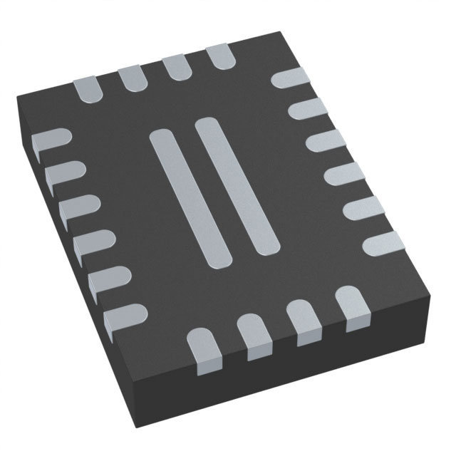
The MP9184 is available in a low-profile 22-pin
3mm x 4mm QFN package.
FEATURES
3V to 20V Wide Input Range
Integrated 10mΩ Low-Side Power FET
SDR Driver for Synchronous Solution
>17A Switch-Current Limit
Up to 97.5% Efficiency
Optional
Internal/External
CurrentSensing Configuration
External Soft Start and Compensation for
Higher Flexibility
Programmable UVLO and Hysteresis
< 1µA Shutdown Current
Thermal Shutdown at 150℃
Available in a 3mm x 4mm QFN-22
Package
APPLICATIONS
USB Type-C
Thunderbolt Interface
Notebooks and Tablets
Bluetooth Audio
Power Banks
Fuel Cells
POS Systems
All MPS parts are lead-free, halogen-free, and adhere to the RoHS directive. For
MPS green status, please visit the MPS website under Quality Assurance.
“MPS” and “The Future of Analog IC Technology” are registered trademarks of
Monolithic Power Systems, Inc.
TYPICAL APPLICATION
100
95
90
85
80
75
70
65
60
55
50
45
40
0.001
MP9184 Rev. 1.0
8/27/2015
VIN=8.4V
VIN=6V
VIN=4.2V
VIN=3V
0.01
0.1
www.MonolithicPower.com
MPS Proprietary Information. Patent Protected. Unauthorized Photocopy and Duplication Prohibited.
© 2015 MPS. All Rights Reserved.
1
10
1
�MP9184 – 17A, 600KHZ, 20V WIDE INPUT RANGE ,SYNCHRONOUS BOOST CONVERTER IN ASMALL 3X4MM QFN PACKAGE
ORDERING INFORMATION
Part Number*
MP9184GL
Package
QFN-22 (3mm×4mm)
Top Marking
See Below
* For Tape & Reel, add suffix –Z (e.g. MP9184GL–Z);
TOP MARKING
MP: MPS prefix:
Y: year code;
W: week code:
9184: first four digits of the part number;
LLL: lot number;
PACKAGE REFERENCE
TOP VIEW
MP9184 Rev. 1.0
8/27/2015
SW
SW
PGND
PGND
20
19
18
17
BST
1
16
AGND
SDR
2
15
SS
OUT
3
14
FB
EN
4
13
COMP
MODE
5
12
VDD
SENSE
6
11
IN
SW
21
PGND
22
7
8
9
10
SW
SW
PGND
PGND
www.MonolithicPower.com
MPS Proprietary Information. Patent Protected. Unauthorized Photocopy and Duplication Prohibited.
© 2015 MPS. All Rights Reserved.
2
�MP9184 – 17A, 600KHZ, 20V WIDE INPUT RANGE ,SYNCHRONOUS BOOST CONVERTER IN ASMALL 3X4MM QFN PACKAGE
ABSOLUTE MAXIMUM RATINGS (1)
Thermal Resistance
(5)
SW .....................–0.3V to +24V (28V for 5.5V). Also, EN can program Vin UVLO. Do not leave EN floating.
Mode Select. Selects the internal or external current sensing mode. Connect to GND to
use internal current-sensing block. If floating, use an external current-sense resistor. DO
NOT pull MODE down to GND through a resistor.
Voltage Sense. Voltage sensed between SENSE and IN. The voltage sensed between
SENSE and IN determines the external current-sense signal.
Power Switch Output. SW is the drain of the internal Power MOSFET. Connect the
power inductor and output rectifier to SW.
Power Ground.
Input Supply. IN must be bypassed locally.
Internal Bias Supply. Decouple with a 2.2μF ceramic capacitor as close to FB as
possible.
Compensation. Connect a capacitor and resistor in series to AGND for loop stability.
Feedback Input. Reference voltage is 1.225V. Connect a resistor divider from VOUT to
FB.
Soft-Start Control. Connect a soft-start capacitor to SS. The soft-start capacitor is
charged with a constant current. Leave SS disconnected if the soft-start is not used.
Analog Ground.
www.MonolithicPower.com
MPS Proprietary Information. Patent Protected. Unauthorized Photocopy and Duplication Prohibited.
© 2015 MPS. All Rights Reserved.
10
�MP9184 – 17A, 600KHZ, 20V WIDE INPUT RANGE ,SYNCHRONOUS BOOST CONVERTER IN ASMALL 3X4MM QFN PACKAGE
FUNCTIONAL BLOCK DIAGRAM
IN
VDD
SENSE
&
+
Internal Regulator
Enable Circuitry
EN
MODE
Charge
Pump
Regulator
Oscillator &
Slope
Current Limit Switch
Control Logic
SW
OUT
BST
SDR
PWM Control
Logic
Boost Strap
Regulator
GND
SR
Driver
SW
Q
FB
7uA
GM
1. 225V
SS
COMP
Figure 1. Functional Block Diagram
MP9184 Rev. 1.0
8/27/2015
www.MonolithicPower.com
MPS Proprietary Information. Patent Protected. Unauthorized Photocopy and Duplication Prohibited.
© 2015 MPS. All Rights Reserved.
11
�MP9184 – 17A, 600KHZ, 20V WIDE INPUT RANGE ,SYNCHRONOUS BOOST CONVERTER IN ASMALL 3X4MM QFN PACKAGE
OPERATION
The MP9184 is a 600kHz fixed-frequency, highefficiency, wide input range, current-mode
boost converter with optional internal or
external current-sensing configuration for highintegration and high-power applications (see
Figure 1).
Boost Function
The MP9184 uses constant frequency, peakcurrent mode, boost regulation architecture to
regulate the feedback voltage.
At the beginning of each cycle, the N-channel
MOSFET switch Q is turned on, forcing the
inductor current to rise. When floating MODE,
the current at the source of switch Q is
measured externally; then it is converted to a
voltage by the current-sense amplifier. That
voltage is compared to the error voltage on
COMP (which is an amplified version of the
difference between the 1.225V reference
voltage and the feedback voltage). When these
two voltages are equal, the PWM comparator
turns off switch Q. This forces the inductor
current into the output capacitor through the
external rectifier, causing the inductor current to
decrease. The peak-inductor current is
controlled by the voltage on COMP, which in
turn is controlled by the output voltage. To
satisfy the load, the output voltage is regulated
by the inductor current. Current mode
regulation improves transient response and
control loop stability.
VDD Power
MP9184 is powered by VDD. A ceramic
capacitor no less than 2.2μF is required to
decouple VDD. During start-up, VDD power is
regulated by IN. Once the output voltage
exceeds the input voltage, VDD is powered
from VOUT (instead of VIN). This allows the
MP9184 to maintain low Ron and high
efficiency, even with low-input voltage.
Soft-Start (SS)
MP9184 uses one external capacitor on SS to
control SW frequency during start-up. The
operation frequency is initially ¼ of the normal
frequency. As the SS capacitor is charged, the
frequency increases continuously. When the
MP9184 Rev. 1.0
8/27/2015
voltage on SS exceeds ~0.65V, the frequency
switches to a normal frequency. In addition, the
voltage on COMP is clamped within VSS+0.7V.
During start-up the COMP voltage reaches
0.7V quickly, and then rises at the same rate of
VSS. These two mechanisms prevent highinrush current from the input power supply.
SDR and BST Function
The MP9184 generates a synchronous gatedriving signal that complements the gate driver
of the internal MOSFET. The SDR driver is
powered from BST (5V, typically) and a low QG
N-channel MOSFET (a gate-source threshold
voltage lower than 3V is preferred). In highpower applications, using a synchronous
rectifier switch improves overall conversion
efficiency. If a synchronous rectifier switch is
not used, float SDR.
The 5V driver power-bootstrap voltage is
powered from OUT. If output voltage is low (or
the duty cycle is too low), BST voltage may not
be regulated to 5V, triggering a BST_UVLO. A
schottky diode from an external 5V source to
BST is recommended, otherwise, the SDR
driver signal may be lost.
Current Sensing Configuration
The MP9184 offers the option of using the
internal circuit or an external resistor to sample
the inductor current. When using the internal
current sense, MODE must be connected
directly to GND before powering on. Meanwhile,
SENSE should be connected to IN. In this
configuration, sensed current is compared to
both the COMP voltage and the limit peak
current cycle-by-cycle during an overload
condition.
When floating MODE, the inductor current is
sampled by an external sense resistor between
IN and SENSE. Under this configuration,
sensed current is compared with COMP for lowside switch on/off control. However, the
overload is protected by the average inductor
current. When the sensed current signal
exceeds 54mV, COMP is pulled low to regulate
the boosted current. This causes the MP9184
to enter hiccup mode (after 1.1ms). The
MP9184 re-starts after about 60ms in hiccup
www.MonolithicPower.com
MPS Proprietary Information. Patent Protected. Unauthorized Photocopy and Duplication Prohibited.
© 2015 MPS. All Rights Reserved.
12
�MP9184 – 17A, 600KHZ, 20V WIDE INPUT RANGE ,SYNCHRONOUS BOOST CONVERTER IN ASMALL 3X4MM QFN PACKAGE
mode. If the sampled current signal rises to
100mV (within the 1.1ms blank time),
immediately the MP9184 operates in hiccup
mode.
The MP9184 starts switching in internal currentsense mode after it detects 0V on MODE. In
external current-sense mode, MP9184 detects
MODE voltage and starts switching (after
MODE is higher than Vin + 2V). In over-current
or hiccup mode, MODE is pulled low. If the
average current limit is triggered before
switching, MP9184 may not start switching
because MODE is regulated to low in an
overload condition.
If the peak-inductor current is higher than 6A,
an external current-sensing resistor is
recommended. Do NOT change the sensing
configuration when MP9184 is in operation.
Light-Load Operation
To optimize efficiency at light load, MP9184
employs a pulse-skipping mechanism and
foldback frequency. When the load becomes
lighter, the COMP voltage decreases, causing
the MP9184 to enter foldback operation (the
lighter the load, the lower the frequency).
However, if the load becomes exceedingly low,
MP9184 enters PSM. PSM operation is
optimized so that only one SW pulse is
launched every burst cycle; therefore the output
ripple is very low.
Enable (EN) and Programmable UVLO
EN enables and disables the MP9184. When
applying voltage higher than the EN higher
threshold (1V, typically), MP9184 starts up
some of the internal circuits (micro-power
mode). If EN voltage exceeds the turn-on
threshold (1.33V), the MP9184 enables all
functions and starts boost operation. Boost
operation is disabled when EN voltage falls
below its lower threshold (1.33V). To
completely shut down the MP9184,