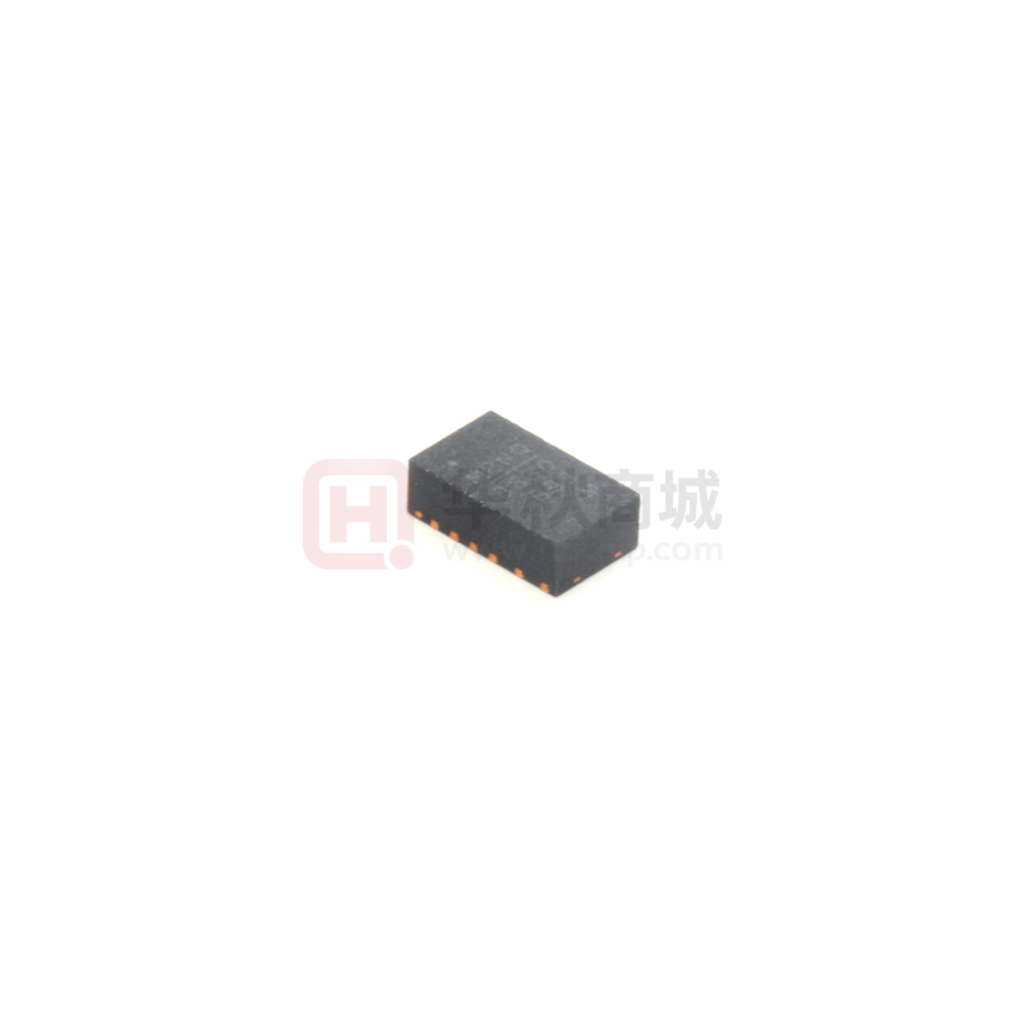
MPM3630
18V/3A DC/DC Module
Synchronous Step-Down Regulator
with Integrated Inductor
The Future of Analog IC Technology
DESCRIPTION
FEATURES
The MPM3630 is a synchronous rectified, stepdown module regulator with built-in power
MOSFETs, inductor, and two capacitors. It
offers a very compact solution to achieve a 3A
continuous output current with excellent load
and line regulation over a wide input supply
range. The MPM3630 has a 1.4MHz switching
frequency, which provides fast load transient
response.
Full protection features include over-current
protection (OCP) and thermal shutdown (TSD).
The MPM3630 eliminates design and
manufacturing
risks
while
dramatically
improving time-to-market.
The MPM3630 is available in a space-saving
QFN20 (3mmx5mmx1.6mm) package.
Complete Switch Mode Power Supply
4.5V to 18V Wide Operating Input Range
3A Continuous Load Current
50mΩ/22mΩ Low RDS(ON) Internal Power
MOSFETs
Integrated Inductor
Fixed 1.4MHz Switching Frequency
1MHz-2MHz Frequency Sync
Internal Power Save Mode for Light Load
Power Good Indicator
OCP Protection and Hiccup
Thermal Shutdown
Output Adjustable from 0.6V
Available in QFN20 (3x5x1.6mm) Package
APPLICATIONS
Industrial Controls
Medical and Imaging Equipment
Telecom Applications
LDO Replacement
Space and Resource-Limited Applications
Distributed Power Systems
All MPS parts are lead-free, halogen-free, and adhere to the RoHS
directive. For MPS green status, please visit MPS website under Quality
Assurance.
“MPS” and “The Future of Analog IC Technology” are Registered
Trademarks of Monolithic Power Systems, Inc.
TYPICAL APPLICATION
MPM3630 Rev. 1.02
www.MonolithicPower.com
5/26/2020
MPS Proprietary Information. Patent Protected. Unauthorized Photocopy and Duplication Prohibited.
© 2020 MPS. All Rights Reserved.
1
�MPM3630 – SYNCHRONOUS STEP-DOWN MODULE WITH INTEGRATED INDUCTOR
ORDERING INFORMATION
Part Number*
MPM3630GQV
Package
QFN-20
(3mmx5mmx1.6mm)
Top Marking
See Below
* For Tape & Reel, add suffix –Z (e.g. MPM3630GQV–Z)
TOP MARKING
MP: MPS prefix
Y: Year code
W: Week code
3630: First four digits of the part number
LLL: Lot number
M: Module
PACKAGE REFERENCE
MPM3630 Rev. 1.02
www.MonolithicPower.com
5/26/2020
MPS Proprietary Information. Patent Protected. Unauthorized Photocopy and Duplication Prohibited.
© 2020 MPS. All Rights Reserved.
2
�MPM3630 – SYNCHRONOUS STEP-DOWN MODULE WITH INTEGRATED INDUCTOR
ABSOLUTE MAXIMUM RATINGS (1)
Thermal Resistance (6)
VIN ................................................... -0.3V to 20V
VOUT ................................................. -0.3V to 20V
VSW .......................................................................
-0.3V (-5V for
1V (when VFB is above 92% of VREF), PG is
pulled high (after a 110 μs delay). During
normal operation, PG is pulled low when the
VFB drops below 81% of VREF (after a 26μs
delay).
Since the MPM3630 doesn’t implement
dedicated output over-voltage protection, PG
will not respond to an output over-voltage
condition.
Over-Current Protection (OCP) and Hiccup
Figure 4: 5.6V Zener Diode Connection
Connecting EN to a voltage source directly
without a pull-up resistor requires limiting the
amplitude of the voltage source to ≤ 5V to
prevent damage to the Zener diode.
Connecting the EN input through a pull-up
resistor to the voltage on VIN limits the EN input
current to less than 100µA.
For example, with 12V connected to VIN,
RPULLUP ≥ (12V – 5.6V) ÷ 100µA = 64kΩ.
For external clock synchronization, connect a
clock with a frequency range between 1MHz
and 2MHz. 2.2ms after the output voltage is set,
the internal clock rising edge will synchronize
with the external clock rising edge. Meanwhile
the width of the high level should be longer than
250ns, and the width of the low level should be
longer than 100ns.
The MPM3630 has a cycle-by-cycle overcurrent limiting control. When the inductor
current peak value exceeds the internal peak
current limit threshold, the HS-FET turns off and
the LS-FET turns on, remaining on until the
inductor current falls below the internal valley
current limit threshold. The valley current limit
circuit is employed to decrease the operation
frequency (after the peak current limit threshold
is triggered). Meanwhile, the output voltage
drops until VFB is below the under-voltage (UV)
threshold (240mV, typically). Once UV is
triggered, the MPM3630 enters hiccup mode to
re-start the part periodically. This protection
mode is useful when the output is dead-shorted
to ground and greatly reduces the average
short-circuit current to alleviate thermal issues
and protect the converter. The MPM3630 exits
hiccup mode once the over-current condition is
removed.
Internal Soft Start (SS)
MPM3630 Rev. 1.02
www.MonolithicPower.com
5/26/2020
MPS Proprietary Information. Patent Protected. Unauthorized Photocopy and Duplication Prohibited.
© 2020 MPS. All Rights Reserved.
12
�MPM3630 – SYNCHRONOUS STEP-DOWN MODULE WITH INTEGRATED INDUCTOR
Thermal Shutdown (TSD)
Thermal shutdown prevents the chip from
operating at exceedingly high temperatures.
When the silicon die reaches temperatures that
exceed 150°C, it shuts down the whole chip.
When the temperature drops below its lower
threshold, typically 130°C, the chip is enabled
again.
Floating Driver and Bootstrap Charging
An internal bootstrap capacitor powers the
floating power MOSFET driver. This floating
driver has its own UVLO protection. This
UVLO’s rising threshold is 2.2V with a
hysteresis of 150mV. The bootstrap capacitor
voltage is regulated internally by VIN through D1,
M1, C4, L1, and C2 (see Figure 5). If (VIN-VSW)
exceeds 5V, U1 will regulate M1 to maintain a
5V BST voltage across C4.
The power dissipation of the RC snubber circuit
is estimated using Equation (1):
PLoss fS CS VIN2
(1)
Where fS is the switching frequency, Cs is the
snubber capacitor, and VIN is the input voltage.
For improved efficiency, the value of CS should
not be set too high. Generally, a 4.99Ω RS and
a 470pF CS are recommended to generate the
RC snubber circuit (see Figure 6).
Figure 6: Additional RC Snubber Circuit
Figure 5: Internal Bootstrap Charging Circuit
Startup and Shutdown
If both VIN and VEN exceed their respective
thresholds, the chip starts up. The reference
block starts first, generating stable reference
voltage, and then the internal regulator is
enabled. The regulator provides a stable supply
for the remaining circuitries.
Three events shut down the chip: VIN low, VEN
low, and thermal shutdown. During the
shutdown procedure, the signaling path is
blocked first to avoid any fault triggering. The
COMP voltage and the internal supply rail are
then pulled down. The floating driver is not
subject to this shutdown command.
Additional RC Snubber Circuit
An additional RC snubber circuit can be chosen
to clamp the voltage spike and damp the ringing
voltage for better EMI performance.
MPM3630 Rev. 1.02
www.MonolithicPower.com
5/26/2020
MPS Proprietary Information. Patent Protected. Unauthorized Photocopy and Duplication Prohibited.
© 2020 MPS. All Rights Reserved.
13
�MPM3630 – SYNCHRONOUS STEP-DOWN MODULE WITH INTEGRATED INDUCTOR
APPLICATION INFORMATION
downgrade when the output voltage is higher
than 5.5V due to thermal concerns.
Setting the Output Voltage
The external resistor divider sets the output
voltage (see Typical Application on page 1).
The feedback resistor R1 also sets the
feedback loop bandwidth with the internal
compensation capacitor (see Figure 7). R2 is
then given using Equation (2):
Selecting the Input Capacitor
The input current to the step-down converter is
discontinuous, therefore it requires a capacitor
to supply the AC current to the step-down
converter while maintaining the DC input
voltage. Use low ESR capacitors for the best
performance. Use ceramic capacitors with X5R
or X7R dielectrics for best results because of
their low ESR and small temperature
coefficients. For most applications, use a 22µF
capacitor.
R2
R1
VOUT
0.6V
(2)
1
Since the capacitor absorbs the input switching
current, it requires an adequate ripple current
rating. The
RMS current in the input capacitor can be
estimated using Equation (3) and Equation (4):
I C1 ILOAD
Figure 7: Feedback Network
Table 1 lists the recommended resistor values
for common output voltages.
Table 1: Resistor Selection for Common Output
Voltages
VOUT
R1
R2
R3
C3
COUT
(µF)
(V)
(kΩ)
(kΩ)
(kΩ)
(pF)
3x22
1.0
51
76.8
51
1.2
51
1.5
1.8
3x22
51
51
51
34
51
51
25.5
0
2.5
51
16
0
2x22
3.3
5
51
51
11.3
6.98
0
2x22
0
2x22
3x22
22
2x22
Normally, it is recommended to set the output
voltage from 0.6V to 5.5V. However, it can be
set higher than 5.5V. In this case, the outputvoltage ripple is larger due to a larger inductor
ripple current. An additional output capacitor is
needed to reduce the output ripple voltage.
If the output voltage is high, heat dissipation
becomes more important. Please refer to the
“PCB Layout Guidelines” section to achieve
better thermal performance. Also, the output will
VOUT VOUT
1
VIN
VIN
(3)
The worst case condition occurs at VIN = 2VOUT,
where:
I C1
ILOAD
2
(4)
To simplifiy, choose an input capacitor with an
RMS current rating greater than half of the
maximum load current.
The input capacitor can be electrolytic, tantalum,
or ceramic. When using electrolytic or tantalum
capacitors, add a small, high-quality ceramic
capacitor (e.g. 0.1μF) placed as close to the IC
as possible. When using ceramic capacitors,
make sure that they have enough capacitance
to provide sufficient charge to prevent
excessive voltage ripple at input. The input
voltage ripple caused by capacitance can be
estimated with Equation (5):
VIN
ILOAD
V
V
OUT 1 OUT
fS C1 VIN
VIN
(5)
Selecting the Output Capacitor
The output capacitor (C2) maintains the DC
output voltage. Use ceramic, tantalum, or lowESR electrolytic capacitors. For best results,
use low ESR capacitors to keep the output
voltage ripple low. The output voltage ripple can
be
estimated
using
Equation
(6):
MPM3630 Rev. 1.02
www.MonolithicPower.com
5/26/2020
MPS Proprietary Information. Patent Protected. Unauthorized Photocopy and Duplication Prohibited.
© 2020 MPS. All Rights Reserved.
14
�MPM3630 – SYNCHRONOUS STEP-DOWN MODULE WITH INTEGRATED INDUCTOR
VOUT
VOUT VOUT
1
1
RESR
fS L1
VIN
8 fS C2
(6)
Where L1 is the inductor value and RESR is the
equivalent series resistance (ESR) value of the
output capacitor, and L1=1µH.
For ceramic capacitors, the capacitance
dominates the impedance at the switching
frequency, and the capacitance causes the
majority of the output voltage ripple. For
simplification, the output voltage ripple can be
estimated using Equation (7):
V
VOUT
(7)
∆V
1 OUT
OUT
8 fS2 L1 C2
VIN
For tantalum or electrolytic capacitors, the ESR
dominates the impedance at the switching
frequency. To simlpify, the output ripple can be
approximated with Equation (8):
∆VOUT
VOUT
V
1 OUT
fS L1
VIN
RESR
Top Layer
(8)
The characteristics of the output capacitor also
affect the stability of the regulation system. The
MPM3630 can be optimized for a wide range of
capacitance and ESR values.
PCB Layout (9)
Efficient PCB layout is critical to achieve stable
operation, especially for input capacitor
placement. For best results, see Figure 8 and
follow the guidelines below:
1.
2.
Place the high current paths GND and IN
very close to the device with short, direct,
and wide traces.
Use a large ground plane to connect
directly to PGND. Add vias near PGND if
the bottom layer is ground plane.
3.
Place the ceramic input capacitor close to
IN and the PGND pins. Keep the
connection of the input capacitor and IN as
short and wide as possible.
4.
Place the external feedback resistors next
to FB.
5.
Keep the feedback network away from the
switching node.
Bottom Layer
Figure 8: Recommended PCB Layout
Notes:
9) The recommended layout is based on the Figure 14 Typical
Application circuit.
MPM3630 Rev. 1.02
www.MonolithicPower.com
5/26/2020
MPS Proprietary Information. Patent Protected. Unauthorized Photocopy and Duplication Prohibited.
© 2020 MPS. All Rights Reserved.
15
�MPM3630 – SYNCHRONOUS STEP-DOWN MODULE WITH INTEGRATED INDUCTOR
Design Example
Below is a design example following the
application guidelines for the specifications
below:
Table 2: Design Example
VIN
VOUT
Io
12V
3.3V
3A
The detailed application schematic is shown in
Figure 14. The typical performance and circuit
waveforms have been shown in the Typical
Performance Characteristics section. For more
device applications, please refer to the related
Evaluation Board Datasheets.
MPM3630 Rev. 1.02
www.MonolithicPower.com
5/26/2020
MPS Proprietary Information. Patent Protected. Unauthorized Photocopy and Duplication Prohibited.
© 2020 MPS. All Rights Reserved.
16
�MPM3630 – SYNCHRONOUS STEP-DOWN MODULE WITH INTEGRATED INDUCTOR
TYPICAL APPLICATION CIRCUITS
Figure 9: Vo = 1V, Io = 3A
Figure 10: Vo = 1.2V, Io = 3A
Figure 11: Vo = 1.5V, Io = 3A
MPM3630 Rev. 1.02
www.MonolithicPower.com
5/26/2020
MPS Proprietary Information. Patent Protected. Unauthorized Photocopy and Duplication Prohibited.
© 2020 MPS. All Rights Reserved.
17
�MPM3630 – SYNCHRONOUS STEP-DOWN MODULE WITH INTEGRATED INDUCTOR
Figure 12: Vo = 1.8V, Io = 3A
BST
SW
VIN
12V
IN
C1
22µF
R4
100k
VOUT
2.5V/3A
MPM3630
OUT
C3
22pF
EN/SYNC
EN
FB
VCC
R5
10k
R2
16K
PG
C2
22µF
C2A
22µF
R1
51K
AGND PGND
Figure 13: Vo = 2.5V, Io = 3A
BST
SW
VIN
12V
IN
C1
22µF
R4
100k
VOUT
3.3V/3A
MPM3630
OUT
C3
22pF
EN/SYNC
EN
R5
10k
FB
VCC
R2
11.3K
PG
C2
22µF
C2A
22µF
R1
51K
AGND PGND
Figure 14: Vo = 3.3V, Io = 3A
MPM3630 Rev. 1.02
www.MonolithicPower.com
5/26/2020
MPS Proprietary Information. Patent Protected. Unauthorized Photocopy and Duplication Prohibited.
© 2020 MPS. All Rights Reserved.
18
�MPM3630 – SYNCHRONOUS STEP-DOWN MODULE WITH INTEGRATED INDUCTOR
Figure 15: Vo = 5, Io = 3A
MPM3630 Rev. 1.02
www.MonolithicPower.com
5/26/2020
MPS Proprietary Information. Patent Protected. Unauthorized Photocopy and Duplication Prohibited.
© 2020 MPS. All Rights Reserved.
19
�MPM3630 – SYNCHRONOUS STEP-DOWN MODULE WITH INTEGRATED INDUCTOR
PACKAGE INFORMATION
QFN-20 (3mmx5mmx1.6mm)
1) ALL DIMENSIONS ARE IN MILLIMETERS.
2) SHADED AREA IS THE KEEP-OUT ZONE. ANY PCB
METAL TRACE AND VIA ARE NOT ALLOWED TO
CONNECT TO THIS AREA ELECTRICALLY OR
MECHANICALLY.
3) LEAD COPLANARITY SHALL BE 0.10
MILLIMETERS MAX.
4) JEDEC REFERENCE IS MO-220.
5) DRAWING IS NOT TO SCALE.
MPM3630 Rev. 1.02
www.MonolithicPower.com
5/26/2020
MPS Proprietary Information. Patent Protected. Unauthorized Photocopy and Duplication Prohibited.
© 2020 MPS. All Rights Reserved.
20
�MPM3630 – SYNCHRONOUS STEP-DOWN MODULE WITH INTEGRATED INDUCTOR
Revision History
Revision
#
Revision
date
Description
R1.02
5/26/2020
we need to correct it to: Analog ground. Reference ground of the logic
circuit. It needs to be connected to PGND on PCB layout.
Pages
Updated
Page 9
NOTICE: The information in this document is subject to change without notice. Users should warrant and guarantee that third
party Intellectual Property rights are not infringed upon when integrating MPS products into any application. MPS will not
assume any legal responsibility for any said applications.
MPM3630 Rev. 1.02
www.MonolithicPower.com
5/26/2020
MPS Proprietary Information. Patent Protected. Unauthorized Photocopy and Duplication Prohibited.
© 2020 MPS. All Rights Reserved.
21
�