MPQ4425M
High Efficiency 1.5A, 36V, 2.2MHz
Synchronous Step-Down LED Driver
AEC-Q100 Qualified
DESCRIPTION
FEATURES
The MPQ4425M is
a
high-frequency,
synchronous, rectified, step-down, switch-mode
white LED driver with built-in power MOSFETs.
It offers a very compact solution to achieve a
1.5A continuous output current with excellent
load and line regulation over a wide input
supply
range.
The
MPQ4425M
has
synchronous mode operation to get high
efficiency.
Current-mode operation provides fast transient
response and eases loop stabilization.
Full protection features include over-current
protection (OCP) and thermal shut down (TSD).
The MPQ4425M requires a minimal number of
readily-available standard external components,
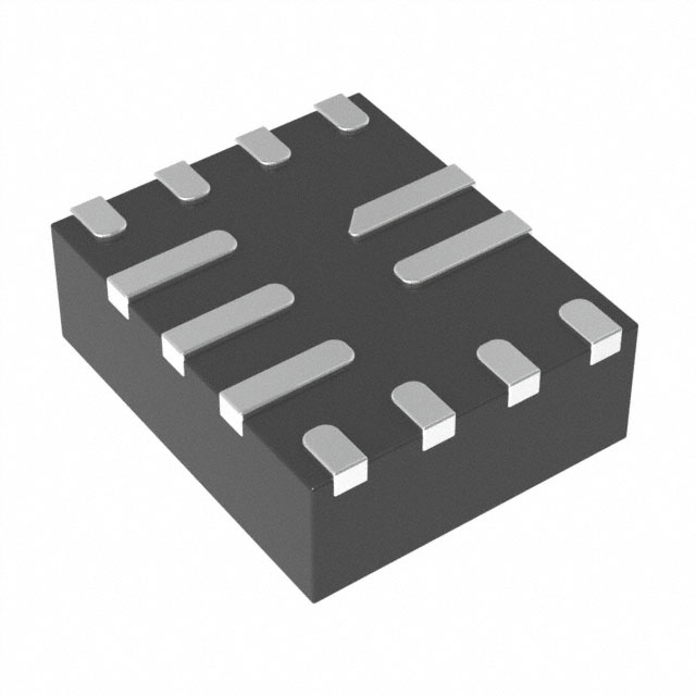
and is available in a space-saving QFN-13
(2.5mmx3mm) package.
EMI Reduction Technique
Wide 4V-to-36V Operating Input Range
85mΩ/50mΩ Low RDS(ON) Internal Power
MOSFETs
High-Efficiency Synchronous Mode
Operation
Default 2.2MHz Switching Frequency
PWM Dimming (Min 100Hz Dimming
Frequency)
Forced CCM Mode
0.2V Reference Voltage
Internal Soft-Start
Fault Indication for LED Short, Open and
Thermal Shutdown
Over-Current Protection (OCP) with ValleyCurrent Detection
Thermal Shutdown
Available in a QFN-13 (2.5mmx3mm)
Package
CISPR25 Class 5 Compliant
Available in a Wettable Flank Package
Available in AEC-Q100 Grade-1
APPLICATIONS
Automotive LED Lighting
All MPS parts are lead-free, halogen free, and adhere to the RoHS
directive. For MPS green status, please visit MPS website under Quality
Assurance.
“MPS” and “The Future of Analog IC Technology” are Registered
Trademarks of Monolithic Power Systems, Inc.
TYPICAL APPLICATION
BST
MPQ4425M
EN/DIM
SW
LED+
FB
LED-
EN/DIM
VCC
/FAULT
/FAULT
PGND AGND
MPQ4425M Rev.1.01
www.MonolithicPower.com
9/30/2017
MPS Proprietary Information. Patent Protected. Unauthorized Photocopy and Duplication Prohibited.
© 2017 MPS. All Rights Reserved.
1
�MPQ4425M – 36V, 1.5A SYNCHRONOUS STEP-DOWN LED DRIVER
ORDERING INFORMATION
Part Number*
MPQ4425MGQB
MPQ4425MGQB-AEC1
MPQ4425MGQBE-AEC1**
Package
QFN-13 (2.5mmx3mm)
Top Marking
See Below
See Below
* For Tape & Reel, add suffix –Z (e.g. MPQ4425MGQB–Z)
** Wettable Flank
TOP MARKING (MPQ4425MGQB & MPQ4425MGQB-AEC1)
ANP: product code;
Y: year code;
WW: week code:
LLL: lot number;
TOP MARKING (MPQ4425MGQBE-AEC1)
AXT: product code;
Y: year code;
WW: week code:
LLL: lot number;
MPQ4425M Rev.1.01
www.MonolithicPower.com
9/30/2017
MPS Proprietary Information. Patent Protected. Unauthorized Photocopy and Duplication Prohibited.
© 2017 MPS. All Rights Reserved.
2
�MPQ4425M – 36V, 1.5A SYNCHRONOUS STEP-DOWN LED DRIVER
PACKAGE REFERENCE
TOP VIEW
IN
IN
PGND
PGND
PGND
BST
13
12
11
10
9
SW
8
AGND
7
VCC
1
2
3
4
5
6
NC
/FAULT
EN
/DIM
FB
QFN-13 (2.5mmx3mm)
ABSOLUTE MAXIMUM RATINGS (1)
Thermal Resistance
Supply voltage (VIN) ....................... -0.3V to 40V
Switch voltage (VSW) ............. -0.3V to VIN + 0.3V
BST voltage (VBST) ................................ VSW+6V
(2)
All other pins ................................ -0.3V to 6V
(3)
Continuous power dissipation (TA = +25°C)
QFN-13 (2.5mmx3mm) ............................ 2.08W
Junction temperature ............................... 150°C
Lead temperature .................................... 260°C
Storage temperature .................. -65°C to 150°C
QFN-13 (2.5mmx3mm) .......... 60 ...... 13 ... °C/W
Recommended Operating Conditions
Supply voltage (VIN) ........................... 4V to 36V
LED current (ILED) .............................. Up to 1.5A
Operating junction temp. (TJ). .. -40°C to +125°C
(4)
θJA
θJC
Notes:
1) Absolute maximum ratings are rated under room temperature
unless otherwise noted. Exceeding these ratings may
damage the device.
2) About the details of EN/DIM pin’s ABS MAX rating, please
refer to page 14, Enable control section.
3) The maximum allowable power dissipation is a function of the
maximum junction temperature TJ (MAX), the junction-toambient thermal resistance θJA, and the ambient temperature
TA. The maximum allowable continuous power dissipation at
any ambient temperature is calculated by PD (MAX) = (TJ
(MAX)-TA)/θJA. Exceeding the maximum allowable power
dissipation will cause excessive die temperature, and the
regulator will go into thermal shutdown. Internal thermal
shutdown circuitry protects the device from permanent
damage.
4) Measured on JESD51-7, 4-layer PCB.
MPQ4425M Rev.1.01
www.MonolithicPower.com
9/30/2017
MPS Proprietary Information. Patent Protected. Unauthorized Photocopy and Duplication Prohibited.
© 2017 MPS. All Rights Reserved.
3
�MPQ4425M – 36V, 1.5A SYNCHRONOUS STEP-DOWN LED DRIVER
ELECTRICAL CHARACTERISTICS
VIN = 12V, VEN = 2V, TJ=-40°C to +125°C, unless otherwise noted, typical values are at TJ=+25°C
Parameter
Symbol
Supply current (shutdown)
Supply current (quiescent)
HS switch-on resistance
LS switch-on resistance
Switch leakage
(5)
Current limit
Reverse current limit
Oscillator frequency
Maximum duty cycle
(5)
IIN
IQ
HSRDS-ON
LSRDS-ON
SW LKG
ILIMIT
VCC =5V
VEN = 0V, VSW =12V
Under 40% Duty Cycle
50
fSW
DMAX
Feedback voltage
VFB
IFB
VEN_RISING
VEN_FALLING
VEN_HYS
IEN
EN turn-off delay
VIN under-voltage lockout
threshold-rising
VIN under-voltage lockout
threshold-falling
VIN under-voltage lockout
threshold-hysteresis
Over
voltage
detection
(/FAULT pulled low)
Over
voltage
detection
hysteresis
/FAULT delay
/FAULT
sink
current
capability
/FAULT leakage current
VCC regulator
VCC load regulation
(5)
Soft-start time
Typ
12
0.6
85
τON_MIN
EN input current
Min
VEN = 0V
VEN = 2V, VFB = 1V, no switching
VBST-SW =5V
Minimum on time
Feedback current
EN rising threshold
EN falling threshold
EN threshold hysteresis
Condition
VFB=100mV
VFB=100mV
2.5
1800
80
4
1.2
2200
87
Max
Units
0.8
150
μA
mA
mΩ
105
1
5.5
2600
mΩ
μA
A
A
kHz
%
46
200
200
30
1.45
1
450
208
216
100
1.8
1.3
VEN=2V
5
10
μA
VEN=0
0.2
50
μA
ms
TJ=+25°C
TJ=-40°C to +125°C
VFB=250mV
192
184
1.1
0.7
ns
mV
nA
V
V
mV
ENtd-off
10
0
25
INUVVth
3.2
3.5
3.8
V
2.8
3.1
3.5
V
INUVHYS
400
mV
FTVth-Hi
140%
VFB
20%
VFB
10
μs
FTTd
VFT
Sink 4mA
IFT-LEAK
VCC
tSS
ICC=0mA
ICC=5mA
ILED=1.5A, L=2.2uH, load=2
series LED, ILED from 10% to
90%
(5)
Thermal shutdown
(5)
Thermal hysteresis
4.6
150
4.9
1.5
0.4
V
100
nA
5.2
4
V
%
0.9
ms
170
30
°C
°C
Note:
5) Derived from bench characterization. Not tested in production
MPQ4425M Rev.1.01
www.MonolithicPower.com
9/30/2017
MPS Proprietary Information. Patent Protected. Unauthorized Photocopy and Duplication Prohibited.
© 2017 MPS. All Rights Reserved.
4
�MPQ4425M – 36V, 1.5A SYNCHRONOUS STEP-DOWN LED DRIVER
PIN FUNCTIONS
Package
Pin #
Name
1, 2
IN
3
NC
4
/FAULT
5
EN/DIM
6
FB
7
VCC
8
AGND
9
SW
10
BST
11, 12,
13
PGND
Description
Supply Voltage. The MPQ4425M operates from a 4V to 36V input rail. Requires CIN to
decouple the input rail. Connect using a wide PCB trace.
Do not connect.
Fault indicator. Open Drain output, pulled to low when LED short, open or thermal
shutdown happening.
Enable/Dimming Control. Pull EN high to enable the MPQ4425M. Apply a 100Hz to 2kHz
external clock to the EN/DIM pin for the PWM dimming.
LED Current Feedback Input.
Internal bias Supply. Decouple VCC with a 0.1μF-to-0.22μF capacitor. The capacitance
should be no more than 0.22μF.
Analog ground. Reference ground of the logic circuit. AGND is connected to PGND
internally. There is no need to add external connections to PGND.
Switch Output. Connect using a wide PCB trace.
Bootstrap. Requires a capacitor connected between SW and BST pins to form a floating
supply across the high-side switch driver. A 20Ω resistor placed between SW and BST cap
is strongly recommended to reduce SW spike voltage.
Power Ground. PGND is the reference ground of the power device and requires careful
consideration during PCB layout. For best results, connect PGND with copper pours and
vias.
MPQ4425M Rev.1.01
www.MonolithicPower.com
9/30/2017
MPS Proprietary Information. Patent Protected. Unauthorized Photocopy and Duplication Prohibited.
© 2017 MPS. All Rights Reserved.
5
�MPQ4425M – 36V, 1.5A SYNCHRONOUS STEP-DOWN LED DRIVER
TYPICAL CHARACTERISTICS
MPQ4425M Rev.1.01
www.MonolithicPower.com
9/30/2017
MPS Proprietary Information. Patent Protected. Unauthorized Photocopy and Duplication Prohibited.
© 2017 MPS. All Rights Reserved.
6
�MPQ4425M – 36V, 1.5A SYNCHRONOUS STEP-DOWN LED DRIVER
TYPICAL PERFORMANCE CHARACTERISTICS
VIN = 12V, LOAD=2 series LED, L=2.2µH, FSW=2.2MHz, TA = +25°C, unless otherwise noted.
MPQ4425M Rev.1.01
www.MonolithicPower.com
9/30/2017
MPS Proprietary Information. Patent Protected. Unauthorized Photocopy and Duplication Prohibited.
© 2017 MPS. All Rights Reserved.
7
�MPQ4425M – 36V, 1.5A SYNCHRONOUS STEP-DOWN LED DRIVER
TYPICAL PERFORMANCE CHARACTERISTICS (continued)
VIN = 12V, LOAD=2 series LED, ILED=1.5A, L=2.2µH, FSW=2.2MHz, with EMI filters, TA = +25°C,
unless otherwise noted. (6)
Amplitude (dBuV/m)
50
45
40
35
30
25
20
15
10
5
0
-5
-10
-15
Data
Class 5 Peak
Class 5 Avg
0.15
5.15
10.15
15.15
20.15
CISPR25 Class 5 Average Radiated Emissions
(150kHz-30MHz)
50
45
40
35
30
25
20
15
10
5
0
-5
-10
-15
Amplitude (dBuV/m)
CISPR25 Class 5 Peak Radiated Emissions
(150kHz-30MHz)
25.15
Data
Class 5 Peak
Class 5 Avg
0.15
5.15
Amplitude (dBuV/m)
Data
Class 5 Peak
Class 5 Avg
0
100
200
300
400
500
600
700
800
900
50
45
40
35
30
25
20
15
10
5
0
-5
-10
-15
100
200
400
500
600
Frequency (MHz)
400
500
600
700
800
900
1000
700
800
900
1000
CISPR25 Class 5 Average Radiated Emissions
(Horizontal, 30MHz-1GHz)
50
45
40
35
30
25
20
15
10
5
0
-5
-10
-15
Amplitude (dBuV/m)
Amplitude (dBuV/m)
Data
Class 5 Peak
Class 5 Avg
300
300
Frequency (MHz)
50
45
40
35
30
25
20
15
10
5
0
-5
-10
-15
200
25.15
Data
Class 5 Peak
Class 5 Avg
0
1000
CISPR25 Class 5 Peak Radiated Emissions
(Horizontal, 30MHz-1GHz)
100
20.15
CISPR25 Class 5 Average Radiated Emissions
(Vertical, 30MHz-1GHz)
Frequency (MHz)
0
15.15
Amplitude (dBuV/m)
CISPR25 Class 5 Peak Radiated Emissions
(Vertical, 30MHz-1GHz)
50
45
40
35
30
25
20
15
10
5
0
-5
-10
-15
10.15
Frequency (MHz)
Frequency (MHz)
Data
Class 5 Peak
Class 5 Avg
0
100
200
300
400
500
600
700
800
900
1000
Frequency (MHz)
MPQ4425M Rev.1.01
www.MonolithicPower.com
9/30/2017
MPS Proprietary Information. Patent Protected. Unauthorized Photocopy and Duplication Prohibited.
© 2017 MPS. All Rights Reserved.
8
�MPQ4425M – 36V, 1.5A SYNCHRONOUS STEP-DOWN LED DRIVER
TYPICAL PERFORMANCE CHARACTERISTICS (continued)
VIN = 12V, LOAD=2 series LED, ILED=1.5A, L=2.2µH, FSW=2.2MHz, with EMI filters, TA = +25°C,
unless otherwise noted. (6)
CISPR25 Class5 Peak Conducted Emissions
(150kHz-108MHz)
CISPR25 Class5 Average Conducted Emissions
(150kHz-108MHz)
Note:
6) The EMC test results are based on application circuit with EMI filters as shown in Figure 9.
MPQ4425M Rev.1.01
www.MonolithicPower.com
9/30/2017
MPS Proprietary Information. Patent Protected. Unauthorized Photocopy and Duplication Prohibited.
© 2017 MPS. All Rights Reserved.
9
�MPQ4425M – 36V, 1.5A SYNCHRONOUS STEP-DOWN LED DRIVER
TYPICAL PERFORMANCE CHARACTERISTICS (continued)
VIN = 12V, LOAD=2 series LED, L=2.2µH, FSW=2.2MHz, TA = +25°C, unless otherwise noted.
MPQ4425M Rev.1.01
www.MonolithicPower.com
9/30/2017
MPS Proprietary Information. Patent Protected. Unauthorized Photocopy and Duplication Prohibited.
© 2017 MPS. All Rights Reserved.
10
�MPQ4425M – 36V, 1.5A SYNCHRONOUS STEP-DOWN LED DRIVER
TYPICAL PERFORMANCE CHARACTERISTICS (continued)
VIN = 12V, LOAD=2 series LED, L=2.2µH, FSW=2.2MHz, TA = +25°C, unless otherwise noted.
MPQ4425M Rev.1.01
www.MonolithicPower.com
9/30/2017
MPS Proprietary Information. Patent Protected. Unauthorized Photocopy and Duplication Prohibited.
© 2017 MPS. All Rights Reserved.
11
�MPQ4425M – 36V, 1.5A SYNCHRONOUS STEP-DOWN LED DRIVER
TYPICAL PERFORMANCE CHARACTERISTICS (continued)
VIN = 12V, LOAD=2 series LED, L=2.2µH, FSW=2.2MHz, TA = +25°C, unless otherwise noted.
MPQ4425M Rev.1.01
www.MonolithicPower.com
9/30/2017
MPS Proprietary Information. Patent Protected. Unauthorized Photocopy and Duplication Prohibited.
© 2017 MPS. All Rights Reserved.
12
�MPQ4425M – 36V, 1.5A SYNCHRONOUS STEP-DOWN LED DRIVER
BLOCK DIAGRAM
Figure 1: Functional Block Diagram
MPQ4425M Rev.1.01
www.MonolithicPower.com
9/30/2017
MPS Proprietary Information. Patent Protected. Unauthorized Photocopy and Duplication Prohibited.
© 2017 MPS. All Rights Reserved.
13
�MPQ4425M – 36V, 1.5A SYNCHRONOUS STEP-DOWN LED DRIVER
OPERATION
The MPQ4425M is
a
high-frequency,
synchronous rectified, step-down, switch-mode
white LED driver with built-in power MOSFETs.
It offers a very compact solution to achieve
1.5A continuous output current with excellent
load and line regulation over a 4V to 36V input
supply range.
The MPQ4425M operates in a fixed-frequency,
peak-current–control mode to regulate the
output current. An internal clock initiates a
PWM cycle. The integrated high-side power
MOSFET turns on and remains on until its
current reaches the value set by the COMP
voltage (VCOMP). When the power switch is off, it
remains off until the next clock cycle starts. If
the current in the power MOSFET does not
reach the current value set by VCOMP within 87%
of one PWM period, the power MOSFET is
forced off.
Internal Regulator
The 4.9V internal regulator power most of the
internal circuitries. This regulator takes the VIN
input and operates in the full VIN range: When
VIN exceeds 4.9V, the output of the regulator is
in full regulation; when VIN falls below 4.9V, the
output decreases following VIN. A 0.1uF
decoupling ceramic capacitor is needed at the
pin.
CCM Operation
The MPQ4425M uses continuous conduction
modulation (CCM) mode to ensure that the part
works with fixed frequency from a no-load to a
full-load range. The advantage of CCM is the
controllable frequency and lower output ripple
at light load.
Frequency Foldback
The MPQ4425M enters frequency foldback
when the input voltage is higher than about 21V.
The frequency decreases to half the nominal
value and changes to 1.1MHz.
Frequency foldback also occurs during soft start
and short-circuit protection.
Error Amplifier (EA)
The error amplifier compares the FB pin voltage
to the internal 0.2V reference (VREF) and
outputs a current proportional to the difference
between the two. This output current then
charges
or
discharges
the
internal
compensation network to form VCOMP, which
controls the power MOSFET current. The
optimized internal compensation network
minimizes the external component counts and
simplifies the control loop design.
Enable Control (EN)
EN/DIM is a control pin that turns the regulator
on and off. Drive EN/DIM high to turn on the
regulator, and drive it low to turn it off. An
internal resistor from EN/DIM to GND allows
EN/DIM to be floated to shut down the chip.
EN/DIM is clamped internally using a 6.5V
series Zener diode (see Figure 2). Connecting
the EN/DIM input through a pull-up resistor to
the voltage on VIN limits the EN input current to
less than 100µA.
For example, with 12V connected to VIN,
RPULLUP ≥ (12V – 6.5V) ÷ 100µA = 55kΩ.
Connecting EN/DIM to a voltage source directly
without a pull-up resistor requires limiting the
amplitude of the voltage source to ≤6V to
prevent damage to the Zener diode.
Figure 2: 6.5V Zener Diode Connection
Drive EN/DIM low longer than 25ms will
shutdown the IC.
PWM Dimming
Apply an external 100Hz to 2kHz PWM
waveform to the EN/DIM pin for PWM dimming.
The average LED current is proportional to
PWM duty. The minimum amplitude of the
PWM signal is 1.8V. If dimming signal is applied
before the chip starts up, the on time of
dimming signal must be longer than 2ms to
make sure the soft start is finished, so output
current can be built. If dimming signal is applied
after soft start is finished, the above 2ms limit is
not required.
Under-Voltage Lockout (UVLO)
Under-voltage lockout (UVLO) protects the chip
from operating at an insufficient supply
MPQ4425M Rev.1.01
www.MonolithicPower.com
9/30/2017
MPS Proprietary Information. Patent Protected. Unauthorized Photocopy and Duplication Prohibited.
© 2017 MPS. All Rights Reserved.
14
�MPQ4425M – 36V, 1.5A SYNCHRONOUS STEP-DOWN LED DRIVER
voltage.The UVLO comparator monitors the
output voltage of the internal regulator (VCC).
drops below its lower threshold (typically
140°C), the chip is enabled again.
Internal Soft Start (SS)
Floating Driver and Bootstrap Charging
The soft start (SS) prevents the converter
output voltage from overshooting during startup. When the chip starts up, the internal
circuitry generates a soft start voltage (VSS).
When VSS is lower than the internal reference
(VREF), VSS overrides VREF, so the error amplifier
uses VSS as the reference. When VSS exceeds
VREF, the error amplifier uses VREF as the
reference.
An external bootstrap capacitor powers the
floating power MOSFET driver. This floating
driver has its own UVLO protection, with a
rising threshold of 2.2V and hysteresis of
150mV. The bootstrap capacitor voltage is
regulated internally by VIN through D1, M1, C3,
L1 and C4 (see Figure 3). If (VIN - VSW) exceeds
5V, U1 regulates M1 to maintain a 5V BST
voltage across C4. As long as VIN is sufficiently
higher than SW, the bootstrap capacitor can be
charged. When the HS-FET is on, VIN≈VSW, so
the bootstrap capacitor cannot be charged.
When the LS-FET is on, VIN - VSW reaches its
maximum for fast charging. When there is no
inductor current, VSW = VOUT, so the difference
between VIN and VOUT can charge the bootstrap
capacitor. A 20Ω resistor placed between SW
and BST cap is strongly recommended to
reduce SW spike voltage.
Fault Indicator
The MPQ4425M has fault indication. The
/FAULT pin is the open drain of a MOSFET. It
should be connected to VCC or some other
voltage source through a resistor (e.g. 100kΩ).
/FAULT pin is pulled high at normal operation,
and LED short, open or thermal shutdown will
pulled down this pin to indicate a fault status.
Over-Current Protection (OCP)
The MPQ4425M has cycle-by-cycle peak
current-limit protection with valley-current
detection. The inductor current is monitored
during the high-side MOSFET (HS-FET) onstate. If the inductor current exceeds the
current-limit value set by the COMP high-clamp
voltage, the HS-FET turns off immediately.
Then the low-side MOSFET (LS-FET) turns on
to discharge the energy, and the inductor
current decreases. The HS-FET remains off
unless the inductor valley current is lower than
a certain current threshold (the valley current
limit), even though the internal clock pulses
high. If the inductor current does not drop below
the valley current limit when the internal clock
pulses high, the HS-FET misses the clock, and
the switching frequency decreases to half the
nominal value. Both the peak and valley current
limits assist in keeping the inductor current from
running away during an overload or short-circuit
condition.
Thermal Shutdown (TSD)
Thermal shutdown prevents the chip from
operating at exceedingly high temperatures.
When the die temperature exceeds 170°C, the
entire chip shuts down. When the temperature
Figure 3: Internal Bootstrap Charging Circuit
Start-up and Shutdown
If both VIN and EN exceed their appropriate
thresholds, the chip starts up. The reference
block starts first, generating stable reference
voltage and currents, and then the internal
regulator is enabled. The regulator provides a
stable supply for the remaining circuitries.
Three events can shut down the chip: VIN low,
EN low, and thermal shutdown. During the
shutdown procedure, the signaling path is first
blocked to avoid any fault triggering. VCOMP and
the internal supply rail are then pulled down.
The floating driver is not subject to this
shutdown command.
MPQ4425M Rev.1.01
www.MonolithicPower.com
9/30/2017
MPS Proprietary Information. Patent Protected. Unauthorized Photocopy and Duplication Prohibited.
© 2017 MPS. All Rights Reserved.
15
�MPQ4425M – 36V, 1.5A SYNCHRONOUS STEP-DOWN LED DRIVER
APPLICATION INFORMATION
Setting the Output Current
The output current is set by the external resistor
RFB (see Figure 4). Feedback reference voltage
is 0.2V, ILED is then given by Equation (1):
I LED
0.2V
R FB
Since CIN absorbs the input switching current, it
requires an adequate ripple current rating. The
RMS current in the input capacitor can be
estimated with Equation (2):
(1)
ICIN ILED
LED+
SW
VOUT
V
(1 OUT )
VIN
VIN
(2)
The worst case condition occurs at VIN = 2VOUT,
shown in Equation (3):
RT
ICIN
FB
RFB
LED-
Figure 4: Feedback Network
RT is used to set the loop bandwidth. Basically,
lower RT, higher bandwidth. But high bandwidth
may cause insufficient phase margin, resulting
in loop unstable. So a proper value of RT is
needed to make a trade-off between bandwidth
and phase margin. Table 1 lists the
recommended feedback resistor and RT values
for common output with 1 or 2 series LED.
Table 1: Resistor Selection for Common Output
ILED (A)
RFB (mΩ)
RT (kΩ)
0.5
400(1%)
200 (1%)
1
200(1%)
150 (1%)
1.5
133(1%)
100 (1%)
Selecting the Input Capacitor
The input current to the step-down converter is
discontinuous, therefore it requires a capacitor
to supply the AC current to the converter while
maintaining the DC input voltage. For the best
performance, use low ESR capacitors. Ceramic
capacitors with X5R or X7R dielectrics are
highly recommended because of their low ESR
and small temperature coefficients.
For most application, use a 4.7µF to 10µF
capacitor. And it is strongly recommended to
use another lower value capacitor (e.g. 0.1µF)
with small package size (0603) to absorb high
frequency switching noise. Make sure place the
small size capacitor as close to IN and GND
pins as possible.
ILED
2
(3)
For simplification, choose an input capacitor
with an RMS current rating greater than half of
the maximum load current.
The input capacitor can be electrolytic, tantalum,
or ceramic. When using electrolytic or tantalum
capacitors, add a small, high-quality ceramic
capacitor (e.g. 0.1μF) as close to the IC as
possible. When using ceramic capacitors,
ensure that they have enough capacitance to
provide a sufficient charge to prevent excessive
voltage ripple at input. The input voltage ripple
caused by capacitance can be estimated with
Equation (4):
VIN
V
V
ILED
OUT (1 OUT )
fSW CIN VIN
VIN
(4)
Selecting the Output Capacitor
The output capacitor maintains the DC output
voltage. Use ceramic, tantalum, or low-ESR
electrolytic capacitors. For best results, use low
ESR capacitors to keep the output voltage
ripple low. The output voltage ripple can be
estimated with Equation (5):
V
V
1
VOUT OUT (1 OUT ) (RESR
) (5)
fSW L
VIN
8fSW COUT
Where L is the inductor value and RESR is the
equivalent series resistance (ESR) value of the
output capacitor.
For ceramic capacitors, the capacitance
dominates the impedance at the switching
frequency, and the capacitance causes the
majority of the output voltage ripple. For
MPQ4425M Rev.1.01
www.MonolithicPower.com
9/30/2017
MPS Proprietary Information. Patent Protected. Unauthorized Photocopy and Duplication Prohibited.
© 2017 MPS. All Rights Reserved.
16
�MPQ4425M – 36V, 1.5A SYNCHRONOUS STEP-DOWN LED DRIVER
simplification, the output voltage ripple can be
estimated with Equation (6):
VOUT
VOUT
V
(1 OUT ) (6)
8 fSW L COUT
VIN
2
For tantalum or electrolytic capacitors, the ESR
dominates the impedance at the switching
frequency. For simplification, the output ripple
can be approximated with Equation (7):
VOUT
V
V
OUT (1 OUT ) RESR
fSW L
VIN
A 1µH to 10µH inductor with a DC current rating
at least 25% higher than the maximum load
current is recommended for most applications.
For higher efficiency, choose an inductor with
lower DC resistance. A larger value inductor
results in less ripple current and a lower output
ripple voltage. However, the larger value
inductor also has a larger physical size, higher
series resistance, and lower saturation current.
A good rule for determining the inductor value is
to allow the inductor ripple current to be
approximately 30% of the maximum load
current. The inductance value can be then be
calculated with Equation (8):
(8)
Where ΔIL is the peak-to-peak inductor ripple
current.
Choose the inductor ripple current to be
approximately 30% of the maximum load
current. The maximum inductor peak current
can be calculated with Equation (9):
ILP ILED
VOUT
V
(1 OUT )
2fSW L
VIN
IN
R UP
EN/DIM
500k
(7)
Selecting the Inductor
VOUT
V
(1 OUT )
fSW IL
VIN
VIN
RDOWN
The characteristics of the output capacitor also
affect the stability of the regulation system. The
MPQ4425M can be optimized for a wide range
of capacitance and ESR values.
L
3.5V while falling threshold is about 3.1V. For
the application needs higher UVLO point,
external resistor divider between IN and
EN/DIM pins can be used to get higher
equivalent UVLO threshold (see Figure 5).
Figure 5: Adjustable UVLO using EN divider
The UVLO threshold can be computed with
Equation (10) and Equation (11):
INUVRISING (1
R UP
) VEN_RISING
500k//R DOWN
(10)
INUVFALLING (1
RUP
) VEN_FALLING
500k//RDOWN
(11)
Where VEN_RISING=1.45V, VEN_FALLING=1V.
When choosing RUP, make sure it is big enough
to limit the current flows into EN/DIM pin lower
than 100uA.
BST Resistor and External BST Diode
A 20ohm resistor in series with BST capacitor is
recommended to reduce the SW spike voltage.
Higher resistance is better for SW spike
reduction, but will compromise the efficiency on
the other hand.
An external BST diode can enhance the
efficiency of the regulator when the duty cycle is
high (>65%). A power supply between 2.5V and
5V can be used to power the external bootstrap
diode and VCC or VOUT is the good choice of
this power supply in the circuit (see Figure 6).
(9)
VIN UVLO Setting
MPQ4425M has internal fixed under-voltage
lockout (UVLO) threshold: rising threshold is
MPQ4425M Rev.1.01
www.MonolithicPower.com
9/30/2017
MPS Proprietary Information. Patent Protected. Unauthorized Photocopy and Duplication Prohibited.
© 2017 MPS. All Rights Reserved.
17
�MPQ4425M – 36V, 1.5A SYNCHRONOUS STEP-DOWN LED DRIVER
Top Layer
Figure 6: Optional External Bootstrap Diode to
Enhance Efficiency
The recommended external BST diode is
IN4148, and the BST capacitor value is 0.1µF
to 1μF.
PCB Layout Guidelines
Inner1 Layer
Efficient PCB layout is critical for stable
operation, especially for input capacitor
placement. For best results, refer to Figure 7
and follow the guidelines below: (7)
1.
Use a large ground plane to connect
directly to PGND. If the bottom layer is a
ground plane, add vias near PGND.
2.
Ensure that the high-current paths at
PGND and IN have short, direct, and wide
traces.
3.
Place the ceramic input capacitor,
especially the small package (0603) input
bypass capacitor as close to IN and PGND
pins as possible to minimize high frequency
noise. Keep the connection of the input
capacitor and IN as short and wide as
possible.
4.
Place the VCC capacitor to VCC pin and
GND pin as close as possible.
5.
Route SW, BST away from sensitive
analog areas such as FB.
6.
Place the feedback resistors close to chip
to ensure the trace which connects to FB
pin as short as possible.
7.
A
four-layer
layout
is
strongly
recommended to achieve better thermal
performance. Use multiple vias to connect
the power planes to internal layers.
Inner2 Layer
Bottom Layer
Figure 7: Recommended PCB Layout
Note:
7) The recommended layout is based on Figure 8.
MPQ4425M Rev.1.01
www.MonolithicPower.com
9/30/2017
MPS Proprietary Information. Patent Protected. Unauthorized Photocopy and Duplication Prohibited.
© 2017 MPS. All Rights Reserved.
18
�MPQ4425M – 36V, 1.5A SYNCHRONOUS STEP-DOWN LED DRIVER
TYPICAL APPLICATION CIRCUIT
4V-36V
VIN
R1
1M
GND
C1A
10µF
1210
50V
C1B
10µF
1210
50V
1, 2
C1C
0.1µF
0603
50V
5
EN/DIM
7
C2
0.1µF
R7
100k
4
R2
10
BST
IN
20
C3
0.1µF
L1
MPQ4425M
EN/DIM
PGND
VCC
9
SW
1.5A
C4
10µF
16V
2.2µH
LED+
11,12,13
R3
6
/FAULT FB
AGND
LED-
100k
R4
400m
1206
8
/FAULT
U1
R6
R5
400m 400m
1206 1206
Figure 8: Io=1.5A Application Circuit
VIN
4V-36V
FB1
1206
VEMI
GND
CIN1 CIN2
1nF 10nF
50V 50V
0603 0603
CIN3
1uF
50V
1206
U1
L1
2.2uH
CIN4
10uF
50V
1210
1, 2
CIN5
10uF
50V
1210
R1
1M
0603
C1A
10uF
1206
50V
C1B
10uF
1206
50V
C1C
0.1uF
0603
50V
5
EN/DIM
7
R7
100K
0603
4
C3
0.1uF/16V
0603
MPQ4425M
EN/DIM
VCC
SW
PGND
R2
20
0603
9
L3
150nH
L2
2.2uH
1.5A
LED+
C4
10uF/16V
1210
C5
1nF/16V
0603
11,12,13
6
/FAULT FB
AGND
R3
200k
0603
8
/FAULT
C2
0.1uF/16V
0603
BST
IN
10
LEDR4
400m
1206
R5
R6
400m 400m
1206 1206
Figure 9: Io=1.5A Application Circuit with EMI Filters
MPQ4425M Rev.1.01
www.MonolithicPower.com
9/30/2017
MPS Proprietary Information. Patent Protected. Unauthorized Photocopy and Duplication Prohibited.
© 2017 MPS. All Rights Reserved.
19
�MPQ4425M – 36V, 1.5A SYNCHRONOUS STEP-DOWN LED DRIVER
PACKAGE INFORMATION
QFN-13 (2.5mmx3mm)
Non-Wettable Flank
PIN 1 ID
MARKING
PIN 1 ID
0.15X45ºTYP
PIN 1 ID
INDEX AREA
BOTTOM VIEW
TOP VIEW
SIDE VIEW
0.15X45º
NOTE:
1) ALL DIMENSIONS ARE IN MILLIMETERS.
2) LEAD COPLANARITY SHALL BE 0.10
MILLIMETERS MAX.
3) JEDEC REFERENCE IS MO-220.
4) DRAWING IS NOT TO SCALE.
RECOMMENDED LAND PATTERN
MPQ4425M Rev.1.01
www.MonolithicPower.com
9/30/2017
MPS Proprietary Information. Patent Protected. Unauthorized Photocopy and Duplication Prohibited.
© 2017 MPS. All Rights Reserved.
20
�MPQ4425M – 36V, 1.5A SYNCHRONOUS STEP-DOWN LED DRIVER
PACKAGE INFORMATION
QFN-13 (2.5mmx3mm)
Wettable Flank
PIN 1 ID
MARKING
PIN 1 ID
0.15X45ºTYP
PIN 1 ID
INDEX AREA
TOP VIEW
BOTTOM VIEW
SIDE VIEW
SECTION A-A
NOTE:
0.15X45º
1) THE LEAD SIDE IS WETTABLE.
2) ALL DIMENSIONS ARE IN MILLIMETERS.
3) LEAD COPLANARITY SHALL BE 0.08
MILLIMETERS MAX.
4) JEDEC REFERENCE IS MO-220.
5) DRAWING IS NOT TO SCALE.
RECOMMENDED LAND PATTERN
NOTICE: The information in this document is subject to change without notice. Please contact MPS for current specifications.
Users should warrant and guarantee that third party Intellectual Property rights are not infringed upon when integrating MPS
products into any application. MPS will not assume any legal responsibility for any said applications.
MPQ4425M Rev. 1.01
www.MonolithicPower.com
9/30/2017
MPS Proprietary Information. Patent Protected. Unauthorized Photocopy and Duplication Prohibited.
© 2017 MPS. All Rights Reserved.
21
�