MPQ4430
36V, 3.5A, Low Quiescent Current,
Synchronous, Step-Down Converter
AEC-Q100 Qualified
The Future of Analog IC Technology
DESCRIPTION
FEATURES
The MPQ4430 is a frequency-programmable
(350kHz to 2.5MHz), synchronous, step-down,
switching regulator with integrated internal highside and low-side power MOSFETs. It provides
up to 3.5A of highly efficient output current with
current mode control for fast loop response.
The wide 3.3V to 36V input range accommodates
a variety of step-down applications in automotive
input environments and is ideal for batterypowered applications due to its extremely low
quiescent current.
The
MPQ4430
employs
advanced
asynchronous mode (AAM), which helps
achieve high efficiency in light-load condition by
scaling down the switching frequency to reduce
switching and gate driving losses.
Standard features include soft start (SS),
external clock synchronization, enable (EN)
control, and a power good (PG) indicator. Highduty cycle and low dropout mode are provided
for automotive cold-crank condition.
Over-current protection (OCP) with valleycurrent detection is employed to prevent the
inductor current from running away. Hiccup
mode reduces the average current in shortcircuit condition greatly. Thermal shutdown
provides reliable and fault-tolerant operation.
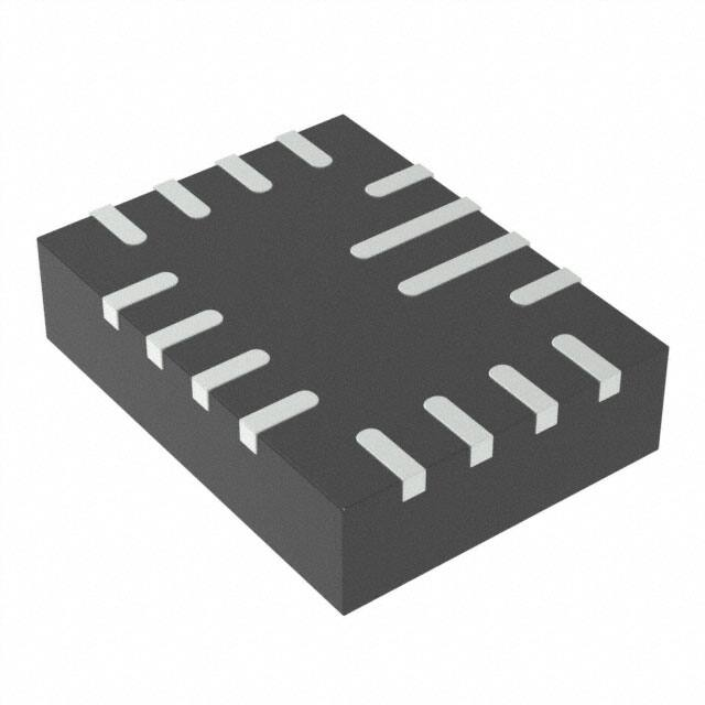
The MPQ4430 is available in a QFN-16
(3mmx4mm) package.
Wide 3.3V to 36V Operating Input Range
3.5A Continuous Output Current
1μA Low Shutdown Mode Current
10μA Sleep Mode Quiescent Current
Internal 90mΩ High-Side and 40mΩ LowSide MOSFETs
350kHz
to
2.5MHz
Programmable
Switching Frequency
Fixed Output Options: 3.3V, 3.8V, 5V
Synchronize to External Clock
Selectable In-Phase or 180° Out-of-Phase
Power Good (PG) Indicator
Programmable Soft-Start (SS) Time
80ns Minimum On Time
Selectable Forced CCM or AAM
Low Dropout Mode
Over-Current Protection (OCP) with ValleyCurrent Detection and Hiccup
Available in a QFN-16 (3mmx4mm)
Package
Available with Wettable Flank
AEC-Q100 Grade 1
APPLICATIONS
Automotive Systems
Industrial Power Systems
All MPS parts are lead-free, halogen-free, and adhere to the RoHS
directive. For MPS green status, please visit the MPS website under
Quality Assurance. “MPS” and “The Future of Analog IC Technology” are
registered trademarks of Monolithic Power Systems, Inc.
TYPICAL APPLICATION
100
95
90
85
80
75
70
65
Output Adjustable Version
MPQ4430 Rev. 1.1
5/28/2020
Output Fixed Version
60
0.01
0.1
www.MonolithicPower.com
MPS Proprietary Information. Patent Protected. Unauthorized Photocopy and Duplication Prohibited.
© 2020 MPS. All Rights Reserved.
1
10
1
�MPQ4430 – 36V, 3.5A, LOW IQ, SYNCHRONOUS, STEP-DOWN CONVERTER
ORDERING INFORMATION
Part Number*
MPQ4430GL
MPQ4430GL-AEC1
MPQ4430GLE-AEC1***
MPQ4430GLE-38-AEC1***
MPQ4430GLE-5-AEC1***
Package
Top Marking
MSL Rating**
See Below
QFN-16 (3mmx4mm)
See Below
See Below
See Below
1
* For Tape & Reel, add suffix –Z (e.g. MPQ4430GL–Z)
** Moisture Sensitivity Level Rating
*** Wettable Flank
TOP MARKING (MPQ4430GL & MPQ4430GL-AEC1)
MP: MPS prefix
Y: Year code
W: Week code
4430: First four digits of the part number
LLL: Lot number
TOP MARKING (MPQ4430GLE-AEC1)
MP: MPS prefix
Y: Year code
W: Week code
4430: First four digits of the part number
LLL: Lot number
E: Wettable lead flank
MPQ4430 Rev. 1.1
5/28/2020
www.MonolithicPower.com
MPS Proprietary Information. Patent Protected. Unauthorized Photocopy and Duplication Prohibited.
© 2020 MPS. All Rights Reserved.
2
�MPQ4430 – 36V, 3.5A, LOW IQ, SYNCHRONOUS, STEP-DOWN CONVERTER
TOP MARKING (MPQ4430GLE-38-AEC1)
MP: MPS prefix
Y: Year code
W: Week code
4430: First four digits of the part number
LLL: Lot number
E: Wettable lead flank
38: 3.8V fixed output
TOP MARKING (MPQ4430GLE-5-AEC1)
MP: MPS prefix
Y: Year code
W: Week code
4430: First four digits of the part number
LLL: Lot number
E: Wettable lead flank
5: 5V fixed output
MPQ4430 Rev. 1.1
5/28/2020
www.MonolithicPower.com
MPS Proprietary Information. Patent Protected. Unauthorized Photocopy and Duplication Prohibited.
© 2020 MPS. All Rights Reserved.
3
�MPQ4430 – 36V, 3.5A, LOW IQ, SYNCHRONOUS, STEP-DOWN CONVERTER
PACKAGE REFERENCE
TOP VIEW
QFN-16 (3mmx4mm)
ABSOLUTE MAXIMUM RATINGS (1)
Supply voltage (VIN) ....................... -0.3V to 40V
Switch voltage (VSW) ............. -0.3V to VIN +0.3V
BST voltage (VBST) .............................VSW + 6.5V
EN voltage (VEN) ............................. -0.3V to 40V
BIAS voltage (VBIAS) ........................ -0.3V to 20V
All other pins ..................................... -0.3V to 6V
Continuous power dissipation (TA = +25°C) (2)
QFN-16 (3mmx4mm) .................................. 2.6W
Junction temperature ................................ 150°C
Lead temperature...................................... 260°C
Storage temperature ................... -65°C to 150°C
Electrostatic Discharge (ESD)
HBM (human body model) .........................±2kV
CDM (charged device model) ................. ±750V
Recommended Operating Conditions
Supply voltage (VIN) ........................ 3.3V to 36V
Operating junction temp. (TJ) (3)
…………………………………...-40°C to +125°C
MPQ4430 Rev. 1.1
5/28/2020
Thermal Resistance
θJA
θJC
QFN-16 (3mmx4mm)
JESD51-7(4) ............................ 48 ...... 11 ... °C/W
EV4430-L-00A (5) ....................43 ....... 5 .... °C/W
NOTES:
1) Absolute maximum ratings are rated under room temperature
unless otherwise noted. Exceeding these ratings may
damage the device.
2) The maximum allowable power dissipation is a function of the
maximum junction temperature TJ(MAX), the junction-toambient thermal resistance θJA, and the ambient temperature
TA. The maximum allowable continuous power dissipation at
any ambient temperature is calculated by PD(MAX)=(TJ(MAX)TA)/ θJA. Exceeding the maximum allowable power dissipation
produces an excessive die temperature, causing the regulator
to go into thermal shutdown. Internal thermal shutdown
circuitry protects the device from permanent damage.
3) Mission profiles requiring operation above 125°C TJ may be
supported; contact MPS for details.
4) Measured on JESD51-7, 4-layer PCB.
5) Measured on EV4430-L-00A, 6.35cm * 6.35cm size, 2oz, 4layer PCB.
www.MonolithicPower.com
MPS Proprietary Information. Patent Protected. Unauthorized Photocopy and Duplication Prohibited.
© 2020 MPS. All Rights Reserved.
4
�MPQ4430 – 36V, 3.5A, LOW IQ, SYNCHRONOUS, STEP-DOWN CONVERTER
ELECTRICAL CHARACTERISTICS
VIN = 12V, VEN = 2V, TJ = -40°C to +125°C, unless otherwise noted. Typical values at TJ = +25°C.
Parameter
Symbol
VIN quiescent current
IQ
VIN shutdown current
ISHDN
VIN under-voltage lockout
threshold rising
VIN under-voltage lockout
threshold hysteresis
Feedback reference voltage
Condition
Min
VOUT
Output voltage accuracy of
MPQ4430-5
VOUT
Switching frequency
fSW
Minimum on time (6)
TON_MIN
SYNC input low voltage
VSYNC_LOW
SYNC input high voltage
VSYNC_HIGH
Units
10
18
10
25
VEN = 0V
1
5
µA
2.8
3.2
V
2.4
150
INUVHYS
Output voltage accuracy of
MPQ4430-38
Max
VFB = 0.85V, no load, no switching,
TJ = +25°C
VFB = 0.85V, no load, no switching
INUVRISING
VREF
Typ
784
TJ = 25°C
TJ = 25°C
TJ = 25°C
RFREQ = 180kΩ or from sync clock
RFREQ = 82kΩ or from sync clock
RFREQ = 27kΩ or from sync clock
800
µA
mV
816
mV
792
800
808
mV
3705
3743
4875
4925
400
850
2250
3800
3800
5000
5000
475
1000
2500
3895
3857
5125
5075
550
1150
2750
mV
mV
mV
mV
kHz
kHz
kHz
80
ns
0.4
V
1.8
V
Current limit
ILIMIT_HS
Duty cycle = 40%
4.7
5.8
7.3
A
Low-side valley current limit
ILIMIT_LS
VOUT = 3.3V, L = 4.7µH
3.1
4.4
5.7
A
ZCD current
Reverse current limit
IZCD
0.1
A
ILIMIT_REVERSE
3
A
Switch leakage current
ISW_LKG
HS switch on resistance
RON_HS
LS switch on resistance
RON_LS
Soft-start current
ISS
EN rising threshold
PGRISING
PG falling threshold
(VFB/VREF)
PGFALLING
PG deglitch timer
TPG_DEGLITCH
PG output voltage low
VCC load regulation
MPQ4430 Rev. 1.1
5/28/2020
1
µA
90
155
mΩ
40
75
mΩ
5
10
15
µA
0.9
1.05
1.2
V
VEN_HYS
PG rising threshold
(VFB/VREF)
VCC regulator
VSS = 0.8V
VEN_RISING
EN threshold hysteresis
0.01
VBST - VSW = 5V
VPG_LOW
120
mV
VFB rising
85
90
95
VFB falling
105
110
115
VFB falling
79
84
89
VFB rising
%
%
113.5 118.5 123.5
%
PG from low to high
30
µs
PG from high to low
50
µs
ISINK = 2mA
0.2
VCC
0.4
5
ICC = 5mA
V
V
3
www.MonolithicPower.com
MPS Proprietary Information. Patent Protected. Unauthorized Photocopy and Duplication Prohibited.
© 2020 MPS. All Rights Reserved.
%
5
�MPQ4430 – 36V, 3.5A, LOW IQ, SYNCHRONOUS, STEP-DOWN CONVERTER
ELECTRICAL CHARACTERISTICS (continued)
VIN = 12V, VEN = 2V, TJ = -40°C to +125°C, unless otherwise noted. Typical values at TJ = +25°C.
Parameter
Thermal shutdown
Symbol
(6)
Thermal shutdown hysteresis
(6)
Condition
Min
Typ
Max
Units
TSD
170
C
TSD_HYS
20
°C
NOTE:
6) Not tested in production and guaranteed by design and characterization.
MPQ4430 Rev. 1.1
5/28/2020
www.MonolithicPower.com
MPS Proprietary Information. Patent Protected. Unauthorized Photocopy and Duplication Prohibited.
© 2020 MPS. All Rights Reserved.
6
�MPQ4430 – 36V, 3.5A, LOW IQ, SYNCHRONOUS, STEP-DOWN CONVERTER
TYPICAL CHARACTERISTICS
VIN = 12V, TJ = -40°C to +125°C, unless otherwise noted.
1.5
20.0
1.4
1.3
15.0
1.2
1.1
1.0
10.0
0.9
0.8
5.0
0.7
0.6
0.0
-50 -30 -10 10 30 50 70 90 110 130
801.0
0.5
-50 -30 -10 10 30 50 70 90 110 130
3.0
2.9
Rising
2.8
2.7
2.6
2.5
Falling
2.4
-50 -30 -10 10 30 50 70 90 110 130
1050
6.0
1030
5.9
1010
5.8
990
5.7
970
5.6
950
-50 -30 -10 10 30 50 70 90 110 130
5.5
-50 -30 -10 10 30 50 70 90 110 130
4.5
150
3.1
4.4
130
4.3
110
4.2
90
4.1
70
4.0
-50 -30 -10 10 30 50 70 90 110 130
50
-50 -30 -10 10 30 50 70 90 110 130
800.5
800.0
799.5
799.0
798.5
798.0
797.5
797.0
-50 -30 -10 10 30 50 70 90 110 130
3.0
2.9
MPQ4430 Rev. 1.1
5/28/2020
2.8
2.7
-50 -30 -10 10 30 50 70 90 110 130
www.MonolithicPower.com
MPS Proprietary Information. Patent Protected. Unauthorized Photocopy and Duplication Prohibited.
© 2020 MPS. All Rights Reserved.
7
�MPQ4430 – 36V, 3.5A, LOW IQ, SYNCHRONOUS, STEP-DOWN CONVERTER
TYPICAL CHARACTERISTICS (continued)
VIN = 12V, TJ = -40°C to +125°C, unless otherwise noted.
150
65
10.2
140
60
10.1
130
55
120
10.0
50
110
100
45
90
40
80
9.9
9.8
9.7
35
70
60
50
-50 -30 -10 10 30 50 70 90 110130
30
9.6
25
-50 -30 -10 10 30 50 70 90110130
9.5
-50 -30 -10 10 30 50 70 90 110130
91.0%
112%
1.05
90.5%
111%
1.00
90.0%
110%
89.5%
109%
1.10
Rising
Falling
0.95
0.90
-50 -30 -10 10 30 50 70 90 110130
89.0%
-50 -30 -10 10 30 50 70 90110130
85.0%
120%
84.5%
119%
84.0%
118%
83.5%
117%
108%
-50 -30 -10 10 30 50 70 90110130
116%
83.0%
-50 -30 -10 10 30 50 70 90110130
MPQ4430 Rev. 1.1
5/28/2020
-50 -30 -10 10 30 50 70 90 110130
www.MonolithicPower.com
MPS Proprietary Information. Patent Protected. Unauthorized Photocopy and Duplication Prohibited.
© 2020 MPS. All Rights Reserved.
8
�MPQ4430 – 36V, 3.5A, LOW IQ, SYNCHRONOUS, STEP-DOWN CONVERTER
TYPICAL PERFORMANCE CHARACTERISTICS
VIN = 12V, VOUT = 5V, Io=3.5A, L = 4.7μH, fSW = 450kHz, with EMI filters, TA = +25°C, unless
otherwise noted. (7)
CISPR25 Class 5 Peak Conducted Emissions CISPR25 Class 5 Average Conducted Emissions
75
70
65
60
55
50
45
40
35
30
25
20
15
10
5
0
-5
-10
-15
-20
150kHz - 108MHz
CISPR25 CLASS 5 LIMITS
AVERAGE CONDUCTED EMI (dBuV)
PEAK CONDUCTED EMI (dBuV)
150kHz -108MHz
NOISE FLOOR
Frequency (MHz)
1
0.1
10
108
75
70
65
60
55
50
45
40
35
30
25
20
15
10
5
0
-5
-10
-15
-20
CISPR25 CLASS 5 LIMITS
NOISE FLOOR
Frequency (MHz)
1
0.1
10
108
CISPR25 Class 5 Peak Radiated Emissions
CISPR25 Class 5 Average Radiated Emissions
150kHz-30MHz
150kHz-30MHz
60
60
55
55
CISPR25 CLASS 5 LIMITS
50
AVERAGE RADIATED EMI (dBuV/m)
PEAK RADIATED EMI (dBuV/m)
50
45
40
35
30
25
20
15
10
NOISE FLOOR
5
0
-5
45
40
35
CISPR25 CLASS 5 LIMITS
30
25
20
15
10
5
0
NOISE FLOOR
-5
-10
-10
1
0.1
Frequency (MHz)
1
0.1
30
Frequency (MHz)
30
CISPR25 Class 5 Peak Radiated Emissions
CISPR25 Class 5 Average Radiated Emissions
Horizontal, 30MHz-200MHz
Horizontal, 30MHz-200MHz
55
55
HORIZONTAL POLARIZATION
50
45
CISPR25 CLASS 5 LIMITS
AVERAGE RADIATED EMI (dBuV/m)
PEAK RADIATED EMI (dBuV/m)
45
HORIZONTAL POLARIZATION
50
40
35
30
25
20
15
10
NOISE FLOOR
5
0
-5
30
40
50
60
70
80
90
100
110
120
130
Frequency (MHz)
MPQ4430 Rev. 1.1
5/28/2020
140
150
160
170
180
190
200
40
35
30
25
CISPR25 CLASS 5 LIMITS
20
15
10
5
0
-5
NOISE FLOOR
30
40
50
60
70
80
90
100
110
120
130
140
150
160
170
180
190
200
Frequency (MHz)
www.MonolithicPower.com
MPS Proprietary Information. Patent Protected. Unauthorized Photocopy and Duplication Prohibited.
© 2020 MPS. All Rights Reserved.
9
�MPQ4430 – 36V, 3.5A, LOW IQ, SYNCHRONOUS, STEP-DOWN CONVERTER
TYPICAL PERFORMANCE CHARACTERISTICS (continued)
VIN = 12V, VOUT = 5V, Io=3.5A, L = 4.7μH, fSW = 450kHz, with EMI filters, TA = +25°C, unless
otherwise noted. (7)
CISPR25 Class 5 Peak Radiated Emissions
CISPR25 Class 5 Average Radiated Emissions
Vertical, 30MHz-200MHz
55
55
VERTICAL POLARIZATION
50
45
CISPR25 CLASS 5 LIMITS
40
35
30
25
20
15
10
NOISE FLOOR
5
0
-5
30
40
50
60
VERTICAL POLARIZATION
50
AVERAGE RADIATED EMI (dBuV/m)
PEAK RADIATED EMI (dBuV/m)
45
Vertical, 30MHz-200MHz
70
80
90
100
110
120
130
140
150
160
170
180
190
40
35
30
25
CISPR25 CLASS 5 LIMITS
20
15
10
5
0
NOISE FLOOR
-5
200
30
Frequency (MHz)
40
50
60
70
80
90
100
110
120
130
140
150
160
170
180
190
200
Frequency (MHz)
CISPR25 Class 5 Peak Radiated Emissions
CISPR25 Class 5 Average Radiated Emissions
Horizontal, 200MHz-1GHz
Horizontal,200MHz-1GHz
55
55
HORIZONTAL POLARIZATION
50
45
45
CISPR25 CLASS 5 LIMITS
AVERAGE RADIATED EMI (dBuV/m)
PEAK RADIATED EMI (dBuV/m)
HORIZONTAL POLARIZATION
50
40
35
30
25
20
15
10
NOISE FLOOR
5
0
-5
200
300
400
500
600
700
800
900
40
35
30
25
CISPR25 CLASS 5 LIMITS
20
15
10
5
0
NOISE FLOOR
-5
1000
200
Frequency (MHz)
300
400
500
600
700
800
900
1000
Frequency (MHz)
CISPR25 Class 5 Peak Radiated Emissions
CISPR25 Class 5 Average Radiated Emissions
Vertical, 200MHz-1GHz
Vertical,200MHz-1GHz
55
55
VERTICAL POLARIZATION
50
AVERAGE RADIATED EMI (dBuV/m)
PEAK RADIATED EMI (dBuV/m)
45
CISPR25 CLASS 5 LIMITS
40
35
30
25
20
15
10
NOISE FLOOR
5
0
-5
200
300
400
VERTICAL POLARIZATION
50
500
600
Frequency (MHz)
700
800
900
1000
45
40
35
30
25
CISPR25 CLASS 5 LIMITS
20
15
10
5
0
NOISE FLOOR
-5
200
300
400
500
600
700
800
900
1000
Frequency (MHz)
NOTE:
7) The EMC test results are based on the application circuit with EMI filters as shown in Figure17.
MPQ4430 Rev. 1.1
5/28/2020
www.MonolithicPower.com
MPS Proprietary Information. Patent Protected. Unauthorized Photocopy and Duplication Prohibited.
© 2020 MPS. All Rights Reserved.
10
�MPQ4430 – 36V, 3.5A, LOW IQ, SYNCHRONOUS, STEP-DOWN CONVERTER
TYPICAL PERFORMANCE CHARACTERISTICS (continued)
VIN = 12V, VOUT = 3.3V, L = 10μH, fSW = 500kHz, AAM, TA = +25°C, unless otherwise noted.
fSW vs. RFREQ
Line Regulation
Load Regulation
0.10
0.03
IOUT =0.5A
0.00
0.05
V IN=12V
0.00
-0.03
V IN=36V
-0.05
IOUT =2A
-0.06
IOUT =3.5A
-0.09
-0.10
V IN=24V
-0.15
-0.20
-0.12
-0.15
-0.25
0
5 10 15 20 25 30 35 40
INPUT VOLTAGE (V)
MPQ4430 Rev. 1.1
5/28/2020
-0.30
0
0.5
1
1.5
2
2.5
3
3.5
LOAD CURRENT (A)
www.MonolithicPower.com
MPS Proprietary Information. Patent Protected. Unauthorized Photocopy and Duplication Prohibited.
© 2020 MPS. All Rights Reserved.
11
�MPQ4430 – 36V, 3.5A, LOW IQ, SYNCHRONOUS, STEP-DOWN CONVERTER
TYPICAL PERFORMANCE CHARACTERISTICS (continued)
VIN = 12V, VOUT = 3.3V, L = 10μH, fSW = 500kHz, AAM, TA = +25°C, unless otherwise noted.
100
95
90
85
80
75
70
65
60
55
50
45
40
0.01
100
95
100
VIN=12V
95
VIN=24V
100
95
VIN=12V
90
90
85
85
80
VIN=12V
80
VIN=24V
VIN=36V
75
0.1
1
LOAD CURRENT (A)
10
70
0.01
75
0.1
1
LOAD CURRENT (A)
10
95
0.1
1
LOAD CURRENT (A)
VIN=12V
95
VIN=12V
90
85
85
80
75
90
90
VIN=24V
VIN=36V
10
100
100
VIN=12V
70
0.01
VIN=24V
85
80
80
75
75
VIN=24V
70
65
60
0.01
0.1
1
LOAD CURRENT (A)
10
70
0.01
90
90
85
85
VIN=12V
80
0.1
1
LOAD CURRENT (A)
10
70
0.01
100
VIN=12V
90
80
75
70
70
65
65
60
60
55
55
40
50
30
45
20
45
40
0.01
VIN=24V
0.1
1
LOAD CURRENT (mA)
MPQ4430 Rev. 1.1
5/28/2020
10
40
0.01
10
VOUT=5V
80
75
50
0.1
1
LOAD CURRENT (A)
70
VIN=24V
0.1
1
LOAD CURRENT (mA)
VOUT=3.3V
60
50
10
10
0.1
1
10
100 1000
LOAD CURRENT (mA)
www.MonolithicPower.com
MPS Proprietary Information. Patent Protected. Unauthorized Photocopy and Duplication Prohibited.
© 2020 MPS. All Rights Reserved.
10000
12
�MPQ4430 – 36V, 3.5A, LOW IQ, SYNCHRONOUS, STEP-DOWN CONVERTER
TYPICAL PERFORMANCE CHARACTERISTICS (continued)
VIN = 12V, VOUT = 3.3V, L = 10μH, fSW = 500kHz, AAM, TA = +25°C, unless otherwise noted.
Efficiency vs. Load Current
Efficiency vs. Load Current
(Extreme Light Load)
(Extreme Light Load)
VIN=14V, FSW=400kHz
90
VIN=14V, FSW=2.2MHz
90
85
85
VOUT=5V
80
80
75
75
70
70
65
80
70
VOUT=3.3V
50
55
55
40
50
50
30
45
45
20
40
0.01
40
0.01
100
0.1
1
LOAD CURRENT (mA)
10
0.1
1
LOAD CURRENT (mA)
VOUT=3.3V
60
60
60
VOUT=5V
90
65
VOUT=3.3V
100
VOUT=5V
10
10
0.1
1
10
100 1000
LOAD CURRENT (mA)
Efficiency vs.
Load Current
Efficiency vs.
Load Current
Efficiency vs.
Load Current
VOUT=3.3V, FSW=500kHz,
Forced CCM Mode
VOUT=3.3V, FSW=2.2MHz,
Forced CCM Mode
VOUT=5V, FSW=500kHz,
Forced CCM Mode
100
VIN=8V
90
90
100
VIN=8V
90
80
80
80
70
70
70
VIN=36V
60
60
50
40
VIN=24V
30
VIN=12V
20
10
0.01
0.1
1
LOAD CURRENT (A)
10
60
VIN=12V
50
50
40
40
30
30
20
20
10
0.01
10
0.01
0.1
1
LOAD CURRENT (A)
10
10000
VIN=8V
VIN=36V
VIN=24V
VIN=12V
0.1
1
LOAD CURRENT (A)
10
Efficiency vs.
Load Current
100
VOUT=5V, FSW=2.2MHz,
Forced CCM Mode
90
VIN=8V
80
70
VIN=12V
60
50
40
30
20
10
0.01
0.1
1
LOAD CURRENT (A)
MPQ4430 Rev. 1.1
5/28/2020
10
www.MonolithicPower.com
MPS Proprietary Information. Patent Protected. Unauthorized Photocopy and Duplication Prohibited.
© 2020 MPS. All Rights Reserved.
13
�MPQ4430 – 36V, 3.5A, LOW IQ, SYNCHRONOUS, STEP-DOWN CONVERTER
TYPICAL PERFORMANCE CHARACTERISTICS (continued)
VIN = 12V, VOUT = 3.3V, L = 10μH, fSW = 500kHz, AAM, TA = +25°C, unless otherwise noted.
50
80
45
70
40
60
50
60
35
30
50
25
40
20
30
15
40
30
20
20
10
5
0
0.0 0.5 1.0 1.5 2.0 2.5 3.0 3.5
10
0
0.0 0.5 1.0 1.5 2.0 2.5 3.0 3.5
10
0
0.0 0.5 1.0 1.5 2.0 2.5 3.0 3.5
50
90
80
45
80
40
70
70
35
60
30
50
25
40
20
15
10
5
0
0.0 0.5 1.0 1.5 2.0 2.5 3.0 3.5
MPQ4430 Rev. 1.1
5/28/2020
60
50
40
30
30
20
20
10
10
0
0.0 0.5 1.0 1.5 2.0 2.5 3.0 3.5
0
0.0 0.5 1.0 1.5 2.0 2.5 3.0 3.5
www.MonolithicPower.com
MPS Proprietary Information. Patent Protected. Unauthorized Photocopy and Duplication Prohibited.
© 2020 MPS. All Rights Reserved.
14
�MPQ4430 – 36V, 3.5A, LOW IQ, SYNCHRONOUS, STEP-DOWN CONVERTER
TYPICAL PERFORMANCE CHARACTERISTICS (continued)
VIN = 12V, VOUT = 3.3V, L = 10μH, fSW = 500kHz, AAM, TA = +25°C, unless otherwise noted.
VOUT/AC
5mV/div.
VOUT/AC
10mV/div.
VOUT/AC
50mV/div.
VSW
10V/div.
IL
200mA/div.
IL
500mA/div.
IL
1A/div.
VSW
5V/div.
VSW
5V/div.
VIN
VIN
VIN
VIN
5V/div.
VIN
5V/div.
VOUT
2V/div.
VIN
5V/div.
VOUT
2V/div.
VOUT
2V/div.
VSW
5V/div.
IL
2A/div.
IL
500mA/div.
VSW
5V/div.
IL
200mA/div.
VSW
10V/div.
VIN
VIN
5V/div.
VOUT
2V/div.
IL
2A/div.
VSW
5V/div.
MPQ4430 Rev. 1.1
5/28/2020
VEN
2V/div.
VOUT
2V/div.
VEN
2V/div.
VOUT
2V/div.
IL
200mA/div.
IL
2A/div.
VSW
10V/div.
VSW
10V/div.
www.MonolithicPower.com
MPS Proprietary Information. Patent Protected. Unauthorized Photocopy and Duplication Prohibited.
© 2020 MPS. All Rights Reserved.
15
�MPQ4430 – 36V, 3.5A, LOW IQ, SYNCHRONOUS, STEP-DOWN CONVERTER
TYPICAL PERFORMANCE CHARACTERISTICS (continued)
VIN = 12V, VOUT = 3.3V, L = 10μH, fSW = 500kHz, AAM, TA = +25°C, unless otherwise noted.
VEN
2V/div.
VOUT
2V/div.
VSW
5V/div.
IL
500mA/div.
VOUT
2V/div.
VPG
5V/div.
IL
5A/div.
VEN
2V/div.
VOUT
2V/div.
IL
5A/div.
VSW
10V/div.
VSW
10V/div.
VEN
2V/div.
VOUT
2V/div.
VOUT
2V/div.
IL
5A/div.
VSW
5V/div.
VOUT
2V/div.
VSYNC
2V/div.
IL
5A/div.
VSW
20V/div.
MPQ4430 Rev. 1.1
5/28/2020
VPG
5V/div.
IL
2A/div.
VSW
20V/div.
VPG
5V/div.
VOUT
2V/div.
IL
2A/div.
VPG
5V/div.
IL
5A/div.
VSW
10V/div.
IL
2A/div.
VOUT
1V/div.
VSYNC
2V/div.
VSW
5V/div.
VSW
5V/div.
www.MonolithicPower.com
MPS Proprietary Information. Patent Protected. Unauthorized Photocopy and Duplication Prohibited.
© 2020 MPS. All Rights Reserved.
16
�MPQ4430 – 36V, 3.5A, LOW IQ, SYNCHRONOUS, STEP-DOWN CONVERTER
TYPICAL PERFORMANCE CHARACTERISTICS (continued)
VIN = 12V, VOUT = 3.3V, L = 10μH, fSW = 500kHz, AAM, TA = +25°C, unless otherwise noted.
3.3V
4.5V
MPQ4430 Rev. 1.1
5/28/2020
www.MonolithicPower.com
MPS Proprietary Information. Patent Protected. Unauthorized Photocopy and Duplication Prohibited.
© 2020 MPS. All Rights Reserved.
17
�MPQ4430 – 36V, 3.5A, LOW IQ, SYNCHRONOUS, STEP-DOWN CONVERTER
TYPICAL PERFORMANCE CHARACTERISTICS (continued)
VIN = 12V, VOUT = 3.3V, L = 10μH, fSW = 500kHz, AAM, TA = +25°C, unless otherwise noted.
MPQ4430 Rev. 1.1
5/28/2020
www.MonolithicPower.com
MPS Proprietary Information. Patent Protected. Unauthorized Photocopy and Duplication Prohibited.
© 2020 MPS. All Rights Reserved.
18
�MPQ4430 – 36V, 3.5A, LOW IQ, SYNCHRONOUS, STEP-DOWN CONVERTER
PIN FUNCTIONS
Pin #
Name
1
PHASE
2
VIN
3, 10
SW
4, 9
PGND
5
EN
6
SYNC
7
PG
8
BIAS
11
BST
12
VCC
13
AGND
14
SS
15
FB
16
FREQ
MPQ4430 Rev. 1.1
5/28/2020
Description
Selectable in-phase or 180° out-of-phase of SYNC input. Drive PHASE high to be
in-phase. Drive PHASE low to be 180° out-of-phase. Recommend to connect this pin
to GND if not used.
Input supply. VIN supplies power to all of the internal control circuitries and the
power switch connected to SW. A decoupling capacitor to ground must be placed
close to VIN to minimize switching spikes.
Switch node. SW is the output of the internal power switch. Pin 3 and Pin 10 are
internally connected.
Power ground. PGND is the reference ground of the power device and requires
careful consideration during PCB layout. For best results, connect PGND with copper
pours and vias.
Enable. Pull EN below the specified threshold to shut the chip down. Pull EN above
the specified threshold to enable the chip.
Synchronize. Apply a 350kHz to 2.5MHz clock signal to SYNC to synchronize the
internal oscillator frequency to the external clock. The external clock should be at
least 250kHz larger than the RFREQ set frequency. SYNC can also be used to select
forced continuous conduction mode (CCM) or advanced asynchronous mode (AAM).
Before the chip starts up, drive SYNC low or leave SYNC floating to choose AAM,
and drive SYNC high to external power source or pull up SYNC to VCC directly to set
the part forced CCM mode.
Power good indicator. The output of PG is an open drain and goes high if the output
voltage is within ±10% of the nominal voltage. Float PG if not used.
External power supply for the internal regulator. Connect BIAS to an external
power supply (5V ≤ VBIAS ≤ 18V) to reduce power dissipation and increase efficiency.
Float BIAS or connect BIAS to ground if not used.
Bootstrap. BST is the positive power supply of the high-side MOSFET driver
connected to SW. Connect a bypass capacitor between BST and SW.
Internal bias supply. VCC supplies power to the internal control circuit and gate
drivers. A ≥1µF decoupling capacitor to ground is required close to VCC.
Analog ground. AGND is the reference ground of the logic circuit.
Soft-start input. Place an external capacitor from SS to AGND to set the soft-start
period. The MPQ4430 sources 10µA from SS to the soft-start capacitor during startup. As the SS voltage rises, the feedback threshold voltage increases to limit inrush
current during start-up. Floating the PIN will activate the internal 0.7ms soft-tart
setting.
Feedback input. For adjustable output version, connect FB to the tap of an external
resistor divider from the output to AGND to set the output voltage. The feedback
threshold voltage is 0.8V. Place the resistor divider as close to FB as possible. Avoid
placing vias on the FB traces. For fixed output version, connect FB pin to the output
directly.
Switching frequency program. Connect a resistor from FREQ to ground to set the
switching frequency.
www.MonolithicPower.com
MPS Proprietary Information. Patent Protected. Unauthorized Photocopy and Duplication Prohibited.
© 2020 MPS. All Rights Reserved.
19
�MPQ4430 – 36V, 3.5A, LOW IQ, SYNCHRONOUS, STEP-DOWN CONVERTER
BLOCK DIAGRAM
Figure 1-1: Functional Block Diagram of Output Adjustable Version
Figure 1-2: Functional Block Diagram of Fixed Output Version
MPQ4430 Rev. 1.1
5/28/2020
www.MonolithicPower.com
MPS Proprietary Information. Patent Protected. Unauthorized Photocopy and Duplication Prohibited.
© 2020 MPS. All Rights Reserved.
20
�MPQ4430 – 36V, 3.5A, LOW IQ, SYNCHRONOUS, STEP-DOWN CONVERTER
TIMING SEQUENCE
VIN
0
SW
0
EN
EN
Threshold
0
VCC
VCC
Threshold
0
118.5% Vref
90% Vref
50% REF 84% Vref
Vo
110% Vref
SS
0
IL=ILimit
IL
0
PG
30µs
50µs
30µs
50µs
30µs
0
Start-Up
N or m al
OCP
N or m al
OV
N o r m al
EN Shutdown
OC
Release
Figure 2: Time Sequence
MPQ4430 Rev. 1.1
5/28/2020
www.MonolithicPower.com
MPS Proprietary Information. Patent Protected. Unauthorized Photocopy and Duplication Prohibited.
© 2020 MPS. All Rights Reserved.
21
�MPQ4430 – 36V, 3.5A, LOW IQ, SYNCHRONOUS, STEP-DOWN CONVERTER
OPERATION
The
MPQ4430
is
a
high-frequency,
synchronous, rectified, step-down, switch-mode
converter with integrated internal high-side and
low-side power MOSFETs. The MPQ4430
offers a very compact solution that achieves
3.5A of continuous output current with excellent
load and line regulation over a wide 3.3V to 36V
input supply range.
The MPQ4430 features a switching frequency
programmable from 350kHz to 2.5MHz,
external soft start, power good indication, and
precision current limit. Its very low operational
quiescent current makes it suitable for batterypowered applications.
Pulse-Width Modulation (PWM) Control
At moderate to high output current, the
MPQ4430 operates in a fixed-frequency, peakcurrent-control mode to regulate the output
voltage. An internal clock initiates a pulse-width
modulation (PWM) cycle. At the rising edge of
the clock, the high-side power MOSFET (HSFET) is turned on, and the inductor current rises
linearly to provide energy to the load. The HSFET remains on until its current reaches the
value set by the COMP voltage (VCOMP), which
is the output of the internal error amplifier. If in
one PWM period, the current in the HS-FET
does not reach VCOMP, the HS-FET remains on,
saving a turn-off operation.
When the HS-FET is off, it remains off until the
next clock cycle begins. The low-side MOSFET
(LS-FET) is turned on immediately while the
inductor current flows through it.
Once the device is in CCM, SYNC can be
pulled low again, or with an external clock if
needed. The advantage of CCM is the
controllable frequency and smaller output ripple,
but it also has low efficiency at light load.
Driving SYNC below its specified threshold
(0.4V) or leaving SYNC floating before the chip
starts up enables AAM power-save mode. The
MPQ4430
first
enters
non-synchronous
operation for as long as the inductor current
approaches zero at light load. If the load is
further decreased or is at no load, then VCOMP is
below the internally set AAM value (VAAM). The
MPQ4430 then enters sleep mode, which
consumes very low quiescent current to further
improve light-load efficiency.
In sleep mode, the internal clock is blocked first,
so the MPQ4430 skips some pulses. Since the
FB voltage (VFB) is lower than the internal 0.8V
reference (VREF) at this time, VCOMP ramps up
until it crosses over VAAM. Then the internal
clock is reset, and the crossover time is taken
as the benchmark of the next clock. This control
scheme helps achieve high efficiency by scaling
down the frequency to reduce switching and
gate driver losses during light-load or no-load
conditions.
When the output current increases from lightload condition, VCOMP becomes larger, and the
switching frequency increases. If the DC value
of VCOMP exceeds VAAM, the operation mode
resumes DCM or CCM, which have a constant
switching frequency.
To prevent shoot-through, a dead time is
inserted to prevent the HS-FET and LS-FET
from being on at the same time. For each turnon and -off in a switching cycle, the HS-FET
turns on or off with minimum on and off time
limit.
Forced CCM and AAM
The
MPQ4430
has
selectable
forced
continuous conduction mode (CCM) and
advanced asynchronous mode (AAM) (see
Figure 3). Driving SYNC higher than its
specified threshold (1.8V) before the chip starts
up forces the device into CCM with a fixed
frequency regardless of the output load current.
MPQ4430 Rev. 1.1
5/28/2020
Figure 3 : Forced CCM and AAM
www.MonolithicPower.com
MPS Proprietary Information. Patent Protected. Unauthorized Photocopy and Duplication Prohibited.
© 2020 MPS. All Rights Reserved.
22
�MPQ4430 – 36V, 3.5A, LOW IQ, SYNCHRONOUS, STEP-DOWN CONVERTER
Error Amplifier (EA)
The error amplifier compares VFB with VREF and
outputs a current proportional to the difference
between the two. This output current then
charges
or
discharges
the
internal
compensation network to form VCOMP, which
controls the power MOSFET current. The
optimized internal compensation network
minimizes the external component count and
simplifies the control loop design.
Internal Regulator and BIAS
Most of the internal circuitry is powered on by
the 5V internal regulator. This regulator takes
the VIN input and operates in the full VIN range.
When VIN exceeds 5V, the output of the
regulator is in full regulation. When VIN falls
below 5V, the output decreases following VIN.
A decoupling ceramic capacitor is needed close
to VCC.
For better thermal performance, connect BIAS
to an external power supply between 5V and
18V. The BIAS supply overrides VIN to power
the internal regulator. Using the BIAS supply
allows VCC to be derived from a high-efficiency
external source, such as VOUT. Float BIAS or
connect BIAS to ground if not used.
Under-Voltage Lockout (UVLO)
Under-voltage lockout (UVLO) protects the chip
from operating at an insufficient supply voltage.
The UVLO comparator monitors the output
voltage of the internal regulator (VCC). The
UVLO rising threshold is about 2.8V with a
150mV hysteresis.
Enable Control (EN)
EN is a digital control pin that turns the
regulator on and off. When EN is pulled below
its threshold voltage, the chip is put into the
lowest shutdown current mode. Pulling EN
above its threshold voltage turns on the part.
Do not float EN.
Power Good Indicator (PG)
The MPQ4430 has a power good (PG) indicator.
PG is the open drain of a MOSFET and should
be connected to VCC or another voltage source
through a resistor (e.g.: 100kΩ). In the
presence of an input voltage, the MOSFET
turns on so that PG is pulled low before SS is
ready. When the regulator output is within
MPQ4430 Rev. 1.1
5/28/2020
±10% of its nominal output, the PG output is
pulled high after a delay, typically 30μs. When
the output voltage moves outside of this range
with a hysteresis, the PG output is pulled low
with a 50μs delay to indicate a failure output
status.
Programmable Frequency
The oscillating frequency of the MPQ4430 can
be programmed either by an external frequency
resistor (RFREQ) or by a logic level synchronous
clock. The frequency resistor should be located
between FREQ and ground as close as to the
device as possible.
The value of RFREQ can be estimated with
Equation (1):
RFREQ (kΩ)
170000
fSW 1.11(kHz)
(1)
The calculated resistance may need fine-tuning
during the bench test.
FREQ is not allowed to be floated even if an
external SYNC clock is added.
SYNC and PHASE
The internal oscillator frequency can be
synchronized to an external clock ranging from
350kHz up to 2.5MHz through SYNC. The
external clock should be at least 250kHz larger
than the RFREQ set frequency. Ensure that the
high amplitude of the SYNC clock is higher than
1.8V, and the low amplitude is lower than 0.4V.
There is no pulse width requirement, but there
is always parasitic capacitance of the pad, so if
the pulse width is too short, a clear rising and
falling edge may not be seen due to the
parasitic capacitance. A pulse longer than
100ns is recommended in application.
PHASE is used when two or more MPQ4430
devices are in parallel with the same SYNC
clock. Pulling PHASE high forces the device to
operate in-phase of the SYNC clock. Pulling it
low forces the device to be 180° out-of-phase of
the SYNC clock. By setting different voltages
for PHASE, two devices can operate 180° outof-phase to reduce the total input current ripple
so a smaller input bypass capacitor can be
used (see Figure 4). The PHASE rising
threshold is about 2.5V with a 400mV
hysteresis.
www.MonolithicPower.com
MPS Proprietary Information. Patent Protected. Unauthorized Photocopy and Duplication Prohibited.
© 2020 MPS. All Rights Reserved.
23
�MPQ4430 – 36V, 3.5A, LOW IQ, SYNCHRONOUS, STEP-DOWN CONVERTER
The MPQ4430 has cycle-by-cycle peak currentlimit protection with valley-current detection and
hiccup mode.
Figure 4 : In-Phase and 180° Out-of-Phase
Soft Start (SS)
Soft start (SS) is implemented to prevent the
converter output voltage from overshooting
during start-up. When the chip starts up, an
internal current source begins charging the
external soft-start capacitor. The internal SS
voltage (VSSI) rises with the soft-start voltage
(VSS), but VSSI is a little different with VSS due to
a 0.5V offset and some delay. When VSS is
lower than 0.5V, VSSI is 0V. VSSI rises from 0V to
0.8V during the period of VSS rises from 0.5V to
1.6V. At this time the error amplifier uses VSSI
as the reference, and the output voltage ramps
up from 0V to the regulated value following VSSI
rising. When VSS reaches 1.6V, VSSI is 0.8V and
overrides the internal VREF, so the error
amplifier uses the internal VREF as the reference.
The soft-start time (tSS) set by the external SS
capacitor can be calculated with Equation (2):
t SS (ms)
CSS (nF) 1.1V
ISS (A)
(2)
Where CSS is the external SS capacitor, and ISS
is the internal 10μA SS charge current. There is
also an internal 0.7ms soft start when SS PIN
float, the final SS time is determined by the
longer time between 0.7ms and external SS
setting time.
SS can be used for tracking and sequencing.
Pre-Bias Start-Up
At start-up, if VFB is higher than VSSI-155mV,
which means the output has a pre-bias voltage,
neither the HS-FET nor the LS-FET are turned
on until VSSI-155mV is higher than VFB.
Over-Current Protection (OCP) and Hiccup
MPQ4430 Rev. 1.1
5/28/2020
The power MOSFET current is accurately
sensed via a current sense MOSFET. It is then
fed to the high-speed current comparator for
current-mode control purposes. During the HSFET on state, if the sensed current exceeds the
peak-current limit value set by the COMP highclamp voltage, the HS-FET turns off
immediately. Then the LS-FET turns on to
discharge the energy, and the inductor current
decreases. The HS-FET remains off unless the
inductor valley current is lower than a certain
current threshold (the valley current limit), even
though the internal clock pulses high. If the
inductor current does not drop below the valley
current limit when the internal clock pulses high,
the HS-FET misses the clock, and the switching
frequency decreases to half the nominal value.
Both the peak and valley current limits assist in
keeping the inductor current from running away
during an overload or short-circuit condition.
When the output is shorted to ground, causing
the output voltage to drop below 55% of its
nominal output, the peak current limit is kicked,
and the device considers this to be an output
dead short and triggers hiccup mode
immediately to restart the part periodically.
In hiccup mode, the MPQ4430 disables its
output power stage and discharges the softstart capacitor slowly. The MPQ4430 restarts
with a full soft-start when the soft-start capacitor
is fully discharged. If the short-circuit condition
still remains after the soft start ends, the device
repeats this operation until the fault is removed
and output returns to the regulation level. This
protection mode reduces the average short
circuit current greatly to alleviate thermal issues
and protect the regulator.
Floating Driver and Bootstrap Charging
A 0.1μF to 1μF external bootstrap capacitor
powers the floating power MOSFET driver. The
floating driver has its own UVLO protection with
a rising threshold of 2.5V and hysteresis of
200mV.
The bootstrap capacitor voltage is charged to
~5V from VCC through a PMOS pass transistor
when the LS-FET is on.
www.MonolithicPower.com
MPS Proprietary Information. Patent Protected. Unauthorized Photocopy and Duplication Prohibited.
© 2020 MPS. All Rights Reserved.
24
�MPQ4430 – 36V, 3.5A, LOW IQ, SYNCHRONOUS, STEP-DOWN CONVERTER
At a high duty cycle operation or sleep mode
condition, the time period available to the
bootstrap charging is less, so the bootstrap
capacitor may not be charged sufficiently. In
case the external circuit does not have
sufficient voltage or time to charge the
bootstrap capacitor, extra external circuitry can
be used to ensure that the bootstrap voltage is
in the normal operation region.
BST Refresh
To improve dropout, the MPQ4430 is designed
to operate at close to 100% duty cycle for as
long as the BST to SW voltage is greater than
2.5V. When the voltage from BST to SW drops
below 2.5V, the HS-FET is turned off using a
UVLO circuit, which forces the LS-FET on to
refresh the charge on the BST capacitor.
Since the supply current sourced from the BST
capacitor is low, the HS-FET can remain on for
more switching cycles than are required to
refresh the capacitor, making the effective duty
cycle of the switching regulator high.
Start-Up and Shutdown
If both VIN and EN exceed their appropriate
thresholds, the chip starts up. The reference
block starts first, generating a stable reference
voltage and current, and then the internal
regulator is enabled. The regulator provides a
stable supply for the rest of the circuitries.
While the internal supply rail is up, an internal
timer holds the power MOSFET off for about
50µs to blank start-up glitches. When the softstart block is enabled, it first holds its SS output
low to ensure that the rest of the circuitries are
ready and slowly ramps up.
Three events can shut down the chip: VIN low,
EN low, and thermal shutdown. During the
shutdown procedure, the signaling path is
blocked first to avoid any fault triggering. VCOMP
and the internal supply rail are then pulled down.
The floating driver is not subject to this
shutdown command, but its charging path is
disabled.
The effective duty cycle during the dropout of
the regulator is mainly influenced by the voltage
drops across the HS-FET, LS-FET, inductor
resistance, and printed circuit board resistance.
In low dropout mode, the COMP is high
clamped; when VIN fast rising, the COMP need
time to jump out high clamped condition, which
may generate overshoot on VOUT; Adjusting the
loop response faster and with bigger COUT
capacitance can help improve the overshoot.
Thermal Shutdown
Thermal shutdown is implemented to prevent
the chip from running away thermally. When the
silicon die temperature exceeds its upper
threshold, the power MOSFETs shut down.
When the temperature drops below its lower
threshold, the chip is enabled again.
MPQ4430 Rev. 1.1
5/28/2020
www.MonolithicPower.com
MPS Proprietary Information. Patent Protected. Unauthorized Photocopy and Duplication Prohibited.
© 2020 MPS. All Rights Reserved.
25
�MPQ4430 – 36V, 3.5A, LOW IQ, SYNCHRONOUS, STEP-DOWN CONVERTER
APPLICATION INFORMATION
Setting the Output Voltage
For adjustable output version, the external
resistor divider connected to FB sets the output
voltage (see Figure 5).
Since CIN absorbs the input switching current, it
requires an adequate ripple current rating. The
RMS current in the input capacitor can be
estimated with Equation (4):
ICIN ILOAD
VOUT
V
(1 OUT )
VIN
VIN
(4)
The worst-case condition occurs at VIN = 2VOUT,
shown in Equation (5):
ICIN
Figure 5: Feedback Network
Choose RFB1 first, then calculate RFB2 with
Equation (3):
R FB2
R FB1
VOUT
1
0.8V
(3)
Table 1 lists the recommended feedback
resistor values for common output voltages.
Table 1: Resistor Selection for Common Output
Voltages
VOUT (V)
RFB1 (kΩ)
RFB2 (kΩ)
3.3
41.2 (1%)
13 (1%)
5
68.1 (1%)
13 (1%)
For fixed output version, connect FB pin to the
output directly.
Selecting the Input Capacitor
The input current to the step-down converter is
discontinuous and therefore requires a
capacitor to supply AC current to the converter
while maintaining the DC input voltage. For the
best performance, use low ESR capacitors.
Ceramic capacitors with X5R or X7R dielectrics
are highly recommended because of their low
ESR and small temperature coefficients.
For most applications, use a 4.7µF to 10µF
capacitor. It is strongly recommended to use
another lower-value capacitor (e.g.: 0.1µF) with
a small package size (0603) to absorb highfrequency switching noise. Place the smaller
capacitor as close to VIN and GND as possible.
MPQ4430 Rev. 1.1
5/28/2020
ILOAD
2
(5)
For simplification, choose an input capacitor
with an RMS current rating greater than half of
the maximum load current.
The input capacitor can be electrolytic, tantalum,
or ceramic. When using electrolytic or tantalum
capacitors, add a small, high-quality ceramic
capacitor (e.g.: 0.1μF) as close to the IC as
possible. When using ceramic capacitors,
ensure that they have enough capacitance to
provide a sufficient charge to prevent excessive
voltage ripple at the input. The input voltage
ripple caused by the capacitance can be
estimated with Equation (6):
VIN
ILOAD
V
V
OUT (1 OUT )
fSW CIN VIN
VIN
(6)
Selecting the Output Capacitor
The output capacitor maintains the DC output
voltage. Use ceramic, tantalum, or low-ESR
electrolytic capacitors. For best results, use low
ESR capacitors to keep the output voltage
ripple low. The output voltage ripple can be
estimated with Equation (7):
V
V
1
) (7)
VOUT OUT (1 OUT ) (RESR
fSW L
VIN
8fSW COUT
Where L is the inductor value, and RESR is the
equivalent series resistance (ESR) value of the
output capacitor.
For ceramic capacitors, the capacitance
dominates the impedance at the switching
frequency and causes the majority of the output
voltage ripple.
www.MonolithicPower.com
MPS Proprietary Information. Patent Protected. Unauthorized Photocopy and Duplication Prohibited.
© 2020 MPS. All Rights Reserved.
26
�MPQ4430 – 36V, 3.5A, LOW IQ, SYNCHRONOUS, STEP-DOWN CONVERTER
For simplification, the output voltage ripple can
be estimated with Equation (8):
VOUT
VOUT
V
(1 OUT ) (8)
8 fSW L COUT
VIN
2
For tantalum or electrolytic capacitors, the ESR
dominates the impedance at the switching
frequency. For simplification, the output ripple
can be approximated with Equation (9):
VOUT
VOUT
V
(1 OUT ) RESR
fSW L
VIN
Selecting the Inductor
A 1µH to 10µH inductor with a DC current rating
at least 25% higher than the maximum load
current is recommended for most applications.
For higher efficiency, choose an inductor with a
lower DC resistance. A larger-value inductor
results in less ripple current and a lower output
ripple voltage, but also has a larger physical
size, higher series resistance, and lower
saturation current. A good rule for determining
the inductor value is to allow the inductor ripple
current to be approximately 30% of the
maximum load current. The inductance value
can then be calculated with Equation (10):
VOUT
V
(1 OUT )
fSW IL
VIN
VIN
VIN
RUP
EN
RDOWN
(9)
The characteristics of the output capacitor also
affect the stability of the regulation system. The
MPQ4430 can be optimized for a wide range of
capacitance and ESR values.
L
higher UVLO point, an external resistor divider
between VIN and EN can be used to achieve a
higher equivalent UVLO threshold (see Figure
6).
Figure 6: Adjustable UVLO Using EN Divider
The UVLO threshold can be calculated with
Equation (12) and Equation (13):
R UP
) VEN_RISING
R DOWN
R UP
(1
) VEN_FALLING
R DOWN
INUVRISING (1
INUVFALLING
(12)
(13)
Where VEN_RISING is 1.05V, and VEN_FALLING is
0.93V.
External BST Diode and Resistor
An external BST diode can enhance the
efficiency of the regulator when the duty cycle is
high. A power supply between 2.5V and 5V can
be used to power the external bootstrap diode.
VCC or VOUT is recommended to be this power
supply in the circuit (see Figure 7).
(10)
Where ∆IL is the peak-to-peak inductor ripple
current.
Choose the inductor ripple current to be
approximately 30% of the maximum load
current. The maximum inductor peak current
can be calculated with Equation (11):
ILP ILOAD
VOUT
V
(1 OUT )
2fSW L
VIN
(11)
VIN UVLO Setting
The MPQ4430 has an internal fixed undervoltage lockout (UVLO) threshold. The rising
threshold is 2.8V, while the falling threshold is
about 2.65V. For the applications that need a
MPQ4430 Rev. 1.1
5/28/2020
Figure 7: Optional External Bootstrap Diode to
Enhance Efficiency
The recommended external BST diode is
IN4148, and the recommended BST capacitor
value is 0.1µF to 1μF. A resistor in series with
the BST capacitor (RBST) can reduce the SW
rising rate and voltage spikes. This helps
enhance EMI performance and reduce voltage
stress at a high VIN. A higher resistance is
better for SW spike reduction but compromises
efficiency. To make a tradeoff between EMI and
efficiency, a ≤20Ω RBST is recommended.
www.MonolithicPower.com
MPS Proprietary Information. Patent Protected. Unauthorized Photocopy and Duplication Prohibited.
© 2020 MPS. All Rights Reserved.
27
�MPQ4430 – 36V, 3.5A, LOW IQ, SYNCHRONOUS, STEP-DOWN CONVERTER
Hot-Plug Application
In a hot-plug application, the VIN pin of the IC
may turn on and off frequently before the power
supply can establish a connection with the IC. In
applications where the input power turns on and
off frequently, the BST capacitor may have a
residual voltage when the IC is turned on. This
may turn on high-side MOSFET (HS-FET) for a
short time before VCC can rise high enough,
which causes an unexpected overshoot on
VOUT.
To protect the IC, hot-plug applications are not
recommended. If a hot-plug application must be
initiated, use a small BST capacitor (e.g. 47nF), a
large VCC capacitor (e.g. 4.7μF), and a large PG
resistor (e.g. 1MΩ) to reduce the overshoot risk.
Contact an MPS FAE to confirm the design.
PCB Layout Guidelines (8)
Efficient PCB layout, especially for input
capacitor placement, is critical for stable
operation. A four-layer layout is strongly
recommended to achieve better thermal
performance. For best results, refer to Figure 8
and follow the guidelines below.
1.
Place symmetric input capacitors as close to
VIN and GND as possible. Recommend to
connect pin1 to GND for symmetric input
structure if in-phase not used. Pin3 and
pin10 are internally connected. Connecting
together on layout or not are both OK.
Recommend to leave pin3 floating for shorter
pin4 and pin1 trace and smaller input hot
loop.
2.
Use a large ground plane to connect to
PGND directly.
3.
Add vias near PGND if the bottom layer is a
ground plane.
4.
Ensure that the high-current paths at GND
and VIN have short, direct, and wide traces.
5.
Place the ceramic input capacitor, especially
the small package size (0603) input bypass
capacitor, as close to VIN and PGND as
possible to minimize high-frequency noise.
6.
Keep the connection of the input capacitor
and VIN as short and wide as possible.
MPQ4430 Rev. 1.1
5/28/2020
7.
Place the VCC capacitor as close to VCC
and GND as possible.
8.
Route SW and BST away from sensitive
analog areas, such as FB.
9.
Place the feedback resistors close to the
chip to ensure that the trace which connects
to FB is as short as possible.
10. Use multiple vias to connect the power
planes to the internal layers.
NOTE:
8) The recommended PCB layout is based on Figure 9.
Top Layer
Inner Layer 1
Inner Layer 2
www.MonolithicPower.com
MPS Proprietary Information. Patent Protected. Unauthorized Photocopy and Duplication Prohibited.
© 2020 MPS. All Rights Reserved.
28
�MPQ4430 – 36V, 3.5A, LOW IQ, SYNCHRONOUS, STEP-DOWN CONVERTER
Bottom Layer
Figure 8: Recommended PCB Layout
MPQ4430 Rev. 1.1
5/28/2020
www.MonolithicPower.com
MPS Proprietary Information. Patent Protected. Unauthorized Photocopy and Duplication Prohibited.
© 2020 MPS. All Rights Reserved.
29
�MPQ4430 – 36V, 3.5A, LOW IQ, SYNCHRONOUS, STEP-DOWN CONVERTER
TYPICAL APPLICATION CIRCUITS
Figure 9: VOUT = 3.3V, fSW = 500kHz
Figure 10: VOUT = 3.3V, fSW = 500kHz for