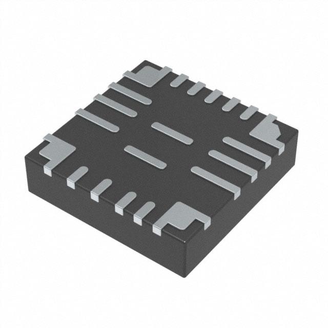
MPQ4491M
The Future of Analog IC Technology
Smart, Single USB Charging Port Power
Converter with Selectable Frequency
for Automotive, AEC-Q100 Qualified
DESCRIPTION
FEATURES
The MPQ4491M integrates a monolithic, stepdown, switch-mode converter and a single USB
current-limit switch with charging port
identification circuits. It achieves 2.5A of
continuous output current with excellent load
and line regulation over a wide input supply
range.
The output of the USB switch is current limited.
The MPQ4491M has a USB dedicate charging
port (DCP) which supports battery charging
specification 1.2 (BC1.2), divider mode, and
1.2V/1.2V mode without the need of outside
user interaction. The output voltage has
programmable line drop compensation.
Full protection features include hiccup current
limiting, output over-voltage protection (OVP), and
thermal shutdown.
The MPQ4491M requires a minimal number of
readily available, standard, external components
and is available in QFN-26 (4mmx4mm) and
QFN-25 (4mmx4mm) packages.
EMI Reduction Technique
14V Typical Operating Input Voltage
36V Max. Operating Input Voltage
Fixed 5V Output Voltage with Line Drop
Compensation
Accurate USB Output Current Limit
40mΩ/32mΩ Low-RDS(ON) Internal Buck
Power MOSFETs
24mΩ Low-RDS(ON) Internal USB Power
MOSFETs
350kHz/250kHz/150kHz Frequency
Selectable
Programmable Line Drop Compensation
Output Over-Voltage Protection (OVP)
Hiccup Current Limit
Supports DCP Schemes for BC1.2, Divider
Mode, and 1.2V/1.2V Mode
±8kV HBM ESD Rating for USB, DP, and
DM
Available in QFN-26 (4mmx4mm) and QFN25 (4mmx4mm) Packages
Available in AEC-Q100 Grade 1
APPLICATIONS
USB Dedicated Charging Ports (DCP)
Automotive Cigarette Lighter Adapters
Power Supply for Linear Chargers
All MPS parts are lead-free, halogen-free, and adhere to the RoHS directive. For
MPS green status, please visit the MPS website under Quality
Assurance. “MPS” and “The Future of Analog IC Technology” are registered
trademarks of Monolithic Power Systems, Inc.
TYPICAL APPLICATION
MPQ4491M Rev. 1.01
www.MonolithicPower.com
6/5/2017
MPS Proprietary Information. Patent Protected. Unauthorized Photocopy and Duplication Prohibited.
© 2017 MPS. All Rights Reserved.
1
�MPQ4491M–SMART, SINGLE USB CHARGING PORT POWER CONVERTER
WITH SELECTABLE FREQUENCY FOR AUTOMOTIVE, AEC-Q100 QUALIFIED
ORDERING INFORMATION
Part Number*
MPQ4491MGR
MPQ4491MGR-AEC1
MPQ4491MGRE
MPQ4491MGRE-AEC1
Package
Top Marking
QFN-26 (4mmx4mm)**
See Below
QFN-25 (4mmx4mm)
See Below
* For Tape & Reel, add suffix –Z (e.g. MPQ4491MGR–Z)
**QFN-26 (4mmx4mm) is not recommended for new designs
TOP MARKING (QFN-26 (4mmx4mm))
MPS: MPS prefix
Y: Year code
WW: Week code
M4491M: Product code of MPQ4491MGR and MPQ4491MGR-AEC1
LLLLLL: Lot number
TOP MARKING (QFN-25 (4mmx4mm))
MPS: MPS prefix
Y: Year code
WW: Week code
M4491M: Product code of MPQ4491MGRE and MPQ4491MGRE-AEC1
LLLLLL: Lot number
E: Part of the suffix
MPQ4491M Rev. 1.01
www.MonolithicPower.com
6/5/2017
MPS Proprietary Information. Patent Protected. Unauthorized Photocopy and Duplication Prohibited.
© 2017 MPS. All Rights Reserved.
2
�MPQ4491M–SMART, SINGLE USB CHARGING PORT POWER CONVERTER
WITH SELECTABLE FREQUENCY FOR AUTOMOTIVE, AEC-Q100 QUALIFIED
PACKAGE REFERENCE
NC
22
21
AGND
NC
23
VCC
DP
24
TOP VIEW
VDROP
DM
TOP VIEW
20
19
18
USB
1
17
NC
USB
2
16
NC
OUT
3
IN
4
PGND
5
15 OUT
25 OUT
14 IN
26 SW
6
7
8
9
10
11
12
PGND
FREQ
EN
SW
SW
BST
PGND
13 PGND
QFN-26 (4mmx4mm)
QFN-25 (4mmx4mm)
ABSOLUTE MAXIMUM RATINGS (1)
Thermal Resistance
Supply voltage (VIN) ..................................... 40V
VSW ......................................................................
-0.3V (-5V for 2V, OC
TJ = -40°C to +125°C
VOUT = 5V, VBUS connected to GND,
TJ = +25°C
VOUT = 5V, VBUS connected to GND,
TJ = -40°C to +125°C
mΩ
A
mV
mV
mV
V
2.5
VMIDDLE
TSS
2.9
500
VCC 0.4V
VHIGH
THICP
On time of hiccup mode
TJ = +25°C
Max load 2.4A, VDROP = float, TJ = +25°C
Max load 2.4A, VDROP = high
Max load 2.4A, VDROP = GND
24
2.75
400
280
130
V
1
1.6
0.4
2.2
0.9
1.6
2.4
50
50
3(7)
70
75
3.5
5
6.5
3
5
7
6.5
8.5
10.5
V
ms
Ω
ms
s
6
8.5
11
125
155
125
160
2.7
2.7
22
22
2.82
2.85
30
34
BC1.2 DCP Mode
DP and DM short
resistance
RDP/DM_Short
VDP = 0.8V, IDM = 1mA, TJ = +25°C
VDP = 0.8V, IDM = 1mA,
TJ = -40°C to +125°C
Ω
Divider Mode
DP/DM output voltage
VDP/DM_Divider
DP/DM output impedance
RDP/DM_Divider
VOUT = 5V, TJ = +25°C
VOUT = 5V, TJ = -40°C to +125°C
TJ = +25°C
TJ = -40°C to +125°C
2.54
2.5
16
14
MPQ4491M Rev. 1.01
www.MonolithicPower.com
6/5/2017
MPS Proprietary Information. Patent Protected. Unauthorized Photocopy and Duplication Prohibited.
© 2017 MPS. All Rights Reserved.
V
kΩ
5
�MPQ4491M–SMART, SINGLE USB CHARGING PORT POWER CONVERTER
WITH SELECTABLE FREQUENCY FOR AUTOMOTIVE, AEC-Q100 QUALIFIED
ELECTRICAL CHARACTERISTICS (continued)
(6)
VIN = 12V, VEN = 5V, TJ = -40°C to +125°C . Typical value is tested at TJ = +25°C, unless
otherwise noted.
Parameter
1.2V/1.2V Mode
Symbol
DP/DM output voltage
VDP/DM_1.2V
DP/DM output impedance
RDP/DM_1.2V
Condition
Min
Typ
Max
VOUT = 5V, TJ = +25°C
VOUT = 5V, TJ = -40°C to +125°C
TJ = +25°C
TJ = -40°C to +125°C
1.16
1.15
55
50
1.25
1.25
68
68
1.34
1.35
80
93
Units
V
kΩ
NOTES:
o
6) All min/max parameters are tested at TJ = 25 C. Limits over temperature are guaranteed by design, characterization, and correlation.
7) Guaranteed by design.
MPQ4491M Rev. 1.01
www.MonolithicPower.com
6/5/2017
MPS Proprietary Information. Patent Protected. Unauthorized Photocopy and Duplication Prohibited.
© 2017 MPS. All Rights Reserved.
6
�MPQ4491M–SMART, SINGLE USB CHARGING PORT POWER CONVERTER
WITH SELECTABLE FREQUENCY FOR AUTOMOTIVE, AEC-Q100 QUALIFIED
TYPICAL PERFORMANCE CHARACTERISTICS
VIN = 12V, VOUT = 5V, L = 22µH, fS = 250kHz, TA = 25°C, unless otherwise noted.
LINE DROP COMPENSATION (mV)
Line Drop Compensation
vs. Load Current
100
450
400
350
95
VDROP=Float
90
300
200
80
VDROP=VCC
100
50
0
0
VIN=12V
85
250
150
Efficiency vs.
Load Current
0.5
1
1.5
2
LOAD CURRENT (A)
VIN=24V
75
VIN=36V
70
VDROP=GND
2.5
VIN=7V
65
0
0.5
1
1.5
2
LOAD CURRENT (A)
2.5
MPQ4491M Rev. 1.01
www.MonolithicPower.com
6/5/2017
MPS Proprietary Information. Patent Protected. Unauthorized Photocopy and Duplication Prohibited.
© 2017 MPS. All Rights Reserved.
7
�MPQ4491M–SMART, SINGLE USB CHARGING PORT POWER CONVERTER
WITH SELECTABLE FREQUENCY FOR AUTOMOTIVE, AEC-Q100 QUALIFIED
TYPICAL PERFORMANCE CHARACTERISTICS (continued)
VIN = 12V, VOUT = 5V, L = 22µH, fS = 250kHz, TA = 25°C, unless otherwise noted.
MPQ4491M Rev. 1.01
www.MonolithicPower.com
6/5/2017
MPS Proprietary Information. Patent Protected. Unauthorized Photocopy and Duplication Prohibited.
© 2017 MPS. All Rights Reserved.
8
�MPQ4491M–SMART, SINGLE USB CHARGING PORT POWER CONVERTER
WITH SELECTABLE FREQUENCY FOR AUTOMOTIVE, AEC-Q100 QUALIFIED
PIN FUNCTIONS
QFN-25
QFN-26
(4mmx4mm) (4mmx4mm)
Pin #
Pin #
1, 23
24
2
1, 2
3, 14, 24
3, 15, 25
4, 13
4, 14
5, 6, 11, 12
5, 6, 12, 13
7
7
8
8
9, 25
9, 10, 26
10
11
15
16, 17
16, 17
18
18
19
19
20
20, 21
21, 22
22
23
Name
Description
D- data line to USB connector. DM is the input/output used for
handshaking with portable devices.
USB
USB output.
Buck output. OUT is the power input for USB. The internal circuit
OUT
senses the OUT voltage and regulates it at 5V.
Supply voltage. IN is the drain of the internal power device and power
supply for the entire chip. The MPQ4491M operates with a 7V to 36V
IN
input voltage. CIN is needed to prevent large voltage spikes at the
input. Place CIN as close to the IC as possible.
Power ground. PGND is the reference ground of the regulated output
PGND voltage and requires extra care during PCB layout. Connect PGND to
GND with copper traces and vias.
Frequency selection. Float FREQ to set the frequency at 150kHz.
FREQ Pull FREQ to ground to set the frequency at 250kHz. Pull FREQ high
to set the frequency at 350kHz.
On/off control input. A 1MΩ resistor is connected between EN and
EN
GND in the internal circuit.
SW
Switch output. Use a wide PCB trace to make the connection.
Bootstrap. Requires a 0.1µF capacitor connected between SW and
BST
BST to form a floating supply across the high-side switch driver.
No connection. NC can be connected to OUT for better thermal
NC
dissipation.
AGND Analog ground. Connect AGND to PGND.
Internal 5V LDO regulator output. Decouple VCC with a 0.22µF
VCC
capacitor.
Line drop compensation selection. Refer to the EC table for detailed
VDROP
specifications.
NC
No connection. NC must be left floating.
D+ data line to USB connector. DP is the input/output used for
DP
handshaking with portable devices.
DM
MPQ4491M Rev. 1.01
www.MonolithicPower.com
6/5/2017
MPS Proprietary Information. Patent Protected. Unauthorized Photocopy and Duplication Prohibited.
© 2017 MPS. All Rights Reserved.
9
�MPQ4491M–SMART, SINGLE USB CHARGING PORT POWER CONVERTER
WITH SELECTABLE FREQUENCY FOR AUTOMOTIVE, AEC-Q100 QUALIFIED
BLOCK DIAGRAM
IN
EN
1MΩ
12KΩ
Current Sense
Amplifier
VCC
Regulator
7.6V
VCC
Oscillator
Σ
Reference
Bootstrap
Regulator
FREQ
HS
Driver
Current Limit
Comparator
Control
Logic
OUT
Rtop
SS
Rbot
VCC
SW
LS
Driver
PGND
Error Amplifier
Line Drop
Compensation
VDROP
BST
OVP Comparator
PWM Comparator
Curent
Sense
USB
Discharge
Charge
Pump
UVLO
Current
Limit
Control
Logic
Thermal
Sense
Discharge
2.7V
AGND
1.2V
DP
Auto
Detect
DM
NC
Figure 1: Functional Block Diagram
MPQ4491M Rev. 1.01
www.MonolithicPower.com
6/5/2017
MPS Proprietary Information. Patent Protected. Unauthorized Photocopy and Duplication Prohibited.
© 2017 MPS. All Rights Reserved.
10
�MPQ4491M–SMART, SINGLE USB CHARGING PORT POWER CONVERTER
WITH SELECTABLE FREQUENCY FOR AUTOMOTIVE, AEC-Q100 QUALIFIED
OPERATION
BUCK CONVERTER SECTION:
The MPQ4491M integrates a monolithic,
synchronous, rectified, step-down, switch-mode
converter with internal power MOSFETs and a
USB current-limit switch with charging port
auto-detection. The MPQ4491 offers a very
compact solution that achieves 2.5A of
continuous output current with excellent load
and line regulation over a wide input supply
range.
The MPQ4491M operates in a fixed-frequency,
peak-current-mode control to regulate the
output voltage. The internal clock initiates the
PWM cycle, which turns on the integrated highside power MOSFET (HS-FET). The HS-FET
turns on and remains on until its current
reaches the value set by the COMP voltage
(VCOMP). If the power switch is off, it remains off
until the next clock cycle begins. If the duty
cycle reaches 88% (350kHz switching
frequency) in one PWM period, the current in
the power MOSFET cannot reach the value set
by VCOMP, and the power MOSFET is forced off.
Error Amplifier (EA)
The error amplifier (EA) compares the internal
feedback voltage against the internal 1V
reference (REF) and outputs a COMP voltage
which controls the power MOSFET current. The
optimized internal compensation network
minimizes the external component count and
simplifies the control loop design.
Internal VCC Regulator
The 5V internal regulator powers most of the
internal circuitries after pulling EN high. This
regulator takes the VIN input and operates in the
full VIN range. When VIN is greater than 5.0V,
the output of the regulator is in full regulation.
When VIN is lower than 5.0V, the output voltage
decreases with VIN. An external 0.22µF ceramic
capacitor is required for decoupling.
Enable Control (EN)
The MPQ4491M has an enable control (EN).
Pull EN high to enable the IC; pull EN low to
disable the IC. Connect EN to VIN through a
resistor for automatic start-up. An internal 1MΩ
resistor connected from EN to GND allows EN
to float to shut down the IC. EN is clamped
internally using a 7.6V series Zener diode (see
Figure 2). Connecting the EN input through a
pull-up resistor to any voltage on VIN limits the
EN input current below 230μA and limits the
amplitude of the voltage source below 10V to
prevent damage to the Zener diode.
For example, if 36V is connected to VIN, then
RPULLUP ≥ (36V – 10V) / 230µA = 113kΩ.
Figure 2: Zener Diode between EN and GND
Under-Voltage Lockout (UVLO)
Under-voltage lockout (UVLO) protects the chip
from operating with an insufficient supply
voltage. The UVLO comparator monitors the
input voltage. The UVLO rising threshold is
5.7V, while its falling threshold is 4.7V.
Internal Soft Start (SS)
The soft start (SS) prevents the converter
output voltage from overshooting during startup. When the chip starts up, the internal
circuitry generates a SS voltage that ramps up
from 0V to 5V. When SS is lower than REF, the
error amplifier uses SS as the reference. When
SS is higher than REF, the error amplifier uses
REF as the reference. The SS time is set to
1.65ms internally.
If the output of the MPQ4491M is pre-biased to
a certain voltage during start-up, the IC disables
the switching of both the high-side and low-side
switches until the voltage on the internal SS
capacitor exceeds the internal feedback voltage.
Buck Over-Current Protection (OCP)
The MPQ4491M has a cycle-by-cycle overcurrent limit for when the inductor peak current
exceeds the current limit threshold and the FB
voltage drops below the under-voltage (UV)
threshold, typically 70% below the reference.
Once UV is triggered, the MPQ4491M enters
hiccup mode to restart the part periodically.
This protection mode is especially useful when
the output is dead-shorted to ground. The
MPQ4491M Rev. 1.01
www.MonolithicPower.com
6/5/2017
MPS Proprietary Information. Patent Protected. Unauthorized Photocopy and Duplication Prohibited.
© 2017 MPS. All Rights Reserved.
11
�MPQ4491M–SMART, SINGLE USB CHARGING PORT POWER CONVERTER
WITH SELECTABLE FREQUENCY FOR AUTOMOTIVE, AEC-Q100 QUALIFIED
average short-circuit current is greatly reduced
to alleviate thermal issues and protect the
regulator. The MPQ4491M exits hiccup mode
once the over-current condition is removed.
Buck Output Over-Voltage Protection (OVP)
The MPQ4491M buck converter has output
over-voltage protection (OVP). If the output is
higher than 6V, the high-side switch stops
turning on, and the low-side switch turns on to
discharge the output voltage until the output
decreases to 5.75V. The chip then resumes
normal operation.
If the output over-voltage cannot be discharged
to 5.75V, the low-side switch turns off after the
inductor current reaches a negative current limit.
The low-side switch turns on again when the
next clock cycle is triggered.
Floating Driver and Bootstrap Charging
An external bootstrap capacitor powers the
floating power MOSFET driver. This floating
driver has its own UVLO protection. The
UVLO’s rising threshold is 2.2V with a
hysteresis of 150mV. The bootstrap capacitor
voltage is regulated internally by VIN through D1,
M1, C4, L1, and C2 (see Figure 3). If VBST -VSW
exceeds 5V, U1 regulates M1 to maintain a 5V
BST voltage across C4.
Start-Up and Shutdown
If both VIN and EN exceed their respective
thresholds, the chip is enabled. The reference
block starts first, generating a stable reference
voltage and current, and then the internal
regulator is enabled. The regulator provides a
stable supply for the remaining circuitries.
Three events can shut down the chip: EN low,
VIN low, and thermal shutdown. During the
shutdown procedure, the signaling path is
blocked first to avoid any fault triggering. The
COMP voltage and the internal supply rail are
then pulled down. The floating driver is not
subject to this shutdown command.
Buck Output Discharge
The buck portion involves a discharge function
that provides a resistive discharge path for the
external output capacitor. The function is active
when the part is disabled (input voltage is under
UVLO, enable off), and is done in a very limited
amount of time. After VCC is discharged below
1V, the buck output discharge resistor is
disconnected.
D1
VIN
M1
BST
5V
U1
C4
VOUT
SW
L1
C2
Figure 3: Internal Bootstrap Charging Circuit
MPQ4491M Rev. 1.01
www.MonolithicPower.com
6/5/2017
MPS Proprietary Information. Patent Protected. Unauthorized Photocopy and Duplication Prohibited.
© 2017 MPS. All Rights Reserved.
12
�MPQ4491M–SMART, SINGLE USB CHARGING PORT POWER CONVERTER
WITH SELECTABLE FREQUENCY FOR AUTOMOTIVE, AEC-Q100 QUALIFIED
USB CURRENT-LIMIT SWITCH SECTION:
MPQ4491M adjusts the OVP threshold based
on different USB loading currents.
Current-Limit Switch
The MPQ4491M integrates a single-channel,
USB current-limit switch that provides built-in,
soft-start circuitry that controls the rising slew
rate of the output voltage to limit inrush current
and voltage surges.
The MPQ4491M uses intelligent line drop
compensation and a dynamic over-voltage
protection control scheme to ensure that the
voltage at the cable terminal meets the 4.75V5.25V specification.
When the load current reaches the current-limit
threshold (typically 2.75A), the USB power
MOSFET switches into foldback current-limit
mode, 70% of the current limit (see Figure 4). If
the over-current limit condition lasts longer than
3ms, the chip enters hiccup mode with a 3ms
on time and an 8.5s off time.
Figure 4: Over-Current Limit
During VIN or EN start-up, the CC load current
cannot exceed 70% of the current limit to avoid
triggering a foldback current limit and causing a
start-up failure.
Output Line Drop Compensation
The MPQ4491M can compensate for an output
voltage drop, such as high impedance caused
by a long trace, to maintain a fairly constant 5V
load-side voltage.
The MPQ4491M uses the internal currentsense output voltage of the current-limit switch
to compensate for the line drop voltage. Since
the trace resistance varies for different cables,
the MPQ4491M provides selectable line drop
compensation through VDROP. The line drop
compensation amplitude increases linearly as
the load current increases, and also has an
upper limitation.
USB Output Over-Voltage Protection (OVP)
The USB switch’s output uses a dynamic overvoltage protection (OVP) threshold to protect
the device at its cable terminal. The
USB Output Discharge
The USB portion involves a discharge function
that provides a resistive discharge path for the
external output capacitor. The function is active
when the part is disabled (input voltage is under
UVLO, enable off), and is done in a very limited
amount of time.
Auto-Detection
The MPQ4491M integrates the USB dedicated
charging port auto-detect function, which
recognizes most mainstream portable devices.
It supports the following charging schemes:
USB battery charging specification BC1.2/
Chinese
Telecommunications
Industry
Standard YD/T 1591-2009
Divider mode
1.2V/1.2V mode
The auto-detect function is a state machine that
supports all of the DCP charging schemes
above.
For MPQ4491MGRE and MPQ4491MGREAEC1, after power startup, it will enter default
divider mode, output voltage is 5.05V with full
line drop compensation. If it enters BC1.2 short
mode or 1.2V/1.2V mode, output voltage will
change to 5.25V with half line drop
compensation. By doing this, the device uses
BC1.2 mode or 1.2V/1.2V mode that can
charge at its full rated current.
For MPQ4491MGR and MPQ4491MGR-AEC1,
the output voltage is always 5.05V with full line
drop compensation no matter which charging
mode it is.
Thermal Shutdown
Thermal shutdown prevents the chip from
operating at exceedingly high temperatures.
When the silicon die temperature exceeds
165°C, the entire chip shuts down. When the
temperature falls below its lower threshold,
typically 145°C, the chip is enabled again.
MPQ4491M Rev. 1.01
www.MonolithicPower.com
6/5/2017
MPS Proprietary Information. Patent Protected. Unauthorized Photocopy and Duplication Prohibited.
© 2017 MPS. All Rights Reserved.
13
�MPQ4491M–SMART, SINGLE USB CHARGING PORT POWER CONVERTER
WITH SELECTABLE FREQUENCY FOR AUTOMOTIVE, AEC-Q100 QUALIFIED
APPLICATION INFORMATION
Selecting the Inductor
Use an inductor with a DC current rating at
least 25% percent higher than the maximum
load current for most applications. Select an
inductor with a small DC resistance for optimum
efficiency. For most designs, the inductor value
can be derived from Equation (1):
L1
VOUT (VIN VOUT )
VIN IL fOSC
(1)
Where ∆IL is the inductor ripple current.
I L
2
(2)
A 22μH toroidal inductor is recommended to
improve EMI.
Selecting the Buck Input Capacitor
The input current to the step-down converter is
discontinuous and therefore requires a
capacitor to supply AC current to the step-down
converter while maintaining the DC input
voltage. For best performance, use low ESR
capacitors. Ceramic capacitors with X5R or
X7R dielectrics are highly recommended
because of their low ESR and small
temperature coefficients. For CLA applications,
a low ESR 100μF electrolytic capacitor and twopiece
10μF
ceramic
capacitors
are
recommended for EMI reduction.
Since the input capacitor (C1) absorbs the input
switching current, it requires an adequate ripple
current rating. The RMS current in the input
capacitor can be estimated with Equation (3):
I C1 ILOAD
VOUT VOUT
1
VIN
VIN
The input capacitor can be electrolytic, tantalum,
or ceramic. When using electrolytic capacitors,
add two high-quality ceramic capacitors as
close to IN as possible. The input voltage ripple
caused by capacitance can be estimated with
Equation (5):
VIN
Choose the inductor ripple current to be
approximately 30% of the maximum load
current. The maximum inductor peak current is
calculated with Equation (2):
IL(MAX ) ILOAD
For simplification, choose an input capacitor
with an RMS current rating greater than half of
the maximum load current.
ILOAD
V
V
OUT 1 OUT
fS C1 VIN
VIN
(5)
Selecting Buck Output Capacitor
The device requires an output capacitor (C2) to
maintain the DC output voltage. Estimate the
output voltage ripple with Equation (6):
VOUT
VOUT VOUT
1
fS L1
VIN
(6)
1
RESR
8
f
C2
S
Where L1 is the inductor value and RESR is the
equivalent series resistance (ESR) value of the
output capacitor.
For electrolytic capacitors, the ESR dominates
the impedance at the switching frequency. For
simplification, the output ripple can be
approximated with Equation (7):
∆VOUT
VOUT
V
1 OUT
fS L1
VIN
RESR
(7)
The characteristics of the output capacitor
affect the stability of the regulatory system. Low
ESR electrolytic capacitors are recommended
for low output ripple and good control loop
stability. For CLA applications, a 1µF ceramic
capacitor and a 270µF polymer or electrolytic
capacitor with ~20mΩ ESR are recommended.
(3)
The worse case condition occurs at VIN = 2VOUT,
shown in Equation (4):
IC1
ILOAD
2
(4)
MPQ4491M Rev. 1.01
www.MonolithicPower.com
6/5/2017
MPS Proprietary Information. Patent Protected. Unauthorized Photocopy and Duplication Prohibited.
© 2017 MPS. All Rights Reserved.
14
�MPQ4491M–SMART, SINGLE USB CHARGING PORT POWER CONVERTER
WITH SELECTABLE FREQUENCY FOR AUTOMOTIVE, AEC-Q100 QUALIFIED
(8)
PCB Layout Guidelines
Efficient PCB layout is critical for stable
operation and thermal dissipation. For best
results, refer to Figure 5 and follow the
guidelines below.
1. Connect OUT using short, direct, and wide
traces. It is highly recommended to add vias
under the IC and route the OUT trace on
both PCB layers.
2. Use a large copper plane for PGND.
Multiple vias should be added for better
thermal dissipation.
4. Use a large copper plane for SW and USB.
5. Place the USB output capacitor close to
USB.
6. Place two ceramic input decoupling
capacitors as close to IN and PGND as
possible to improve EMI performance.
7. Place the VCC decoupling capacitor as
close to VCC as possible.
NOTES:
8) The recommended layout is based on Figure 6: Typical
Application Circuit on the next page.
3. Connect AGND to PGND.
Top Layer
Mid1 Layer
USB
GND
BUCK Vo
VIN
GND
Mid2 Layer
Bottom Layer
Figure 5: Recommended Layout
MPQ4491M Rev. 1.01
www.MonolithicPower.com
6/5/2017
MPS Proprietary Information. Patent Protected. Unauthorized Photocopy and Duplication Prohibited.
© 2017 MPS. All Rights Reserved.
15
�MPQ4491M–SMART, SINGLE USB CHARGING PORT POWER CONVERTER
WITH SELECTABLE FREQUENCY FOR AUTOMOTIVE, AEC-Q100 QUALIFIED
TYPICAL APPLICATION CIRCUITS
10
Figure 6: VIN = 7V ‐ 36V, USB = 5V/2.5A
NOTE: The typical application circuit is based on the QFN-25 (4mmx4mm).
MPQ4491M Rev. 1.01
www.MonolithicPower.com
6/5/2017
MPS Proprietary Information. Patent Protected. Unauthorized Photocopy and Duplication Prohibited.
© 2017 MPS. All Rights Reserved.
16
�MPQ4491M–SMART, SINGLE USB CHARGING PORT POWER CONVERTER
WITH SELECTABLE FREQUENCY FOR AUTOMOTIVE, AEC-Q100 QUALIFIED
PACKAGE INFORMATION
QFN-26 (4mmx4mm)
MPQ4491M Rev. 1.01
www.MonolithicPower.com
6/5/2017
MPS Proprietary Information. Patent Protected. Unauthorized Photocopy and Duplication Prohibited.
© 2017 MPS. All Rights Reserved.
17
�MPQ4491M–SMART, SINGLE USB CHARGING PORT POWER CONVERTER
WITH SELECTABLE FREQUENCY FOR AUTOMOTIVE, AEC-Q100 QUALIFIED
QFN-25 (4mmx4mm)
NOTICE: The information in this document is subject to change without notice. Users should warrant and guarantee that third
party Intellectual Property rights are not infringed upon when integrating MPS products into any application. MPS will not
assume any legal responsibility for any said applications.
MPQ4491M Rev.1.0
www.MonolithicPower.com
6/5/2017
MPS Proprietary Information. Patent Protected. Unauthorized Photocopy and Duplication Prohibited.
© 2017 MPS. All Rights Reserved.
18
�