MPQ6533
Three-Channel Automotive Pre-Driver,
AEC-100 Qualified
DESCRIPTION
FEATURES
The MPQ6533 is a gate driver IC designed for
automotive DC motor driver applications. The
device drives six N-channel power MOSFETs to
drive DC motors or other loads.
•
•
•
The MPQ6533 integrates an LDO regulator to
generate gate drive voltages for the low-side
MOSFETs. The device also provides a charge
pump that generates a voltage to drive an
external N-channel MOSFET for reverse battery
protection. The high-side gate drive is
generated by the bootstrap capacitors and an
internal charge pump, which allows for 100%
duty cycle operation.
•
•
•
•
•
•
•
•
•
•
An internal amplifier measures the voltage drop
across the low-side MOSFETs. This allows the
current to be measured without using shunt
resistors.
•
Integrated LDO Regulator for Gate Drive
Charge Pump for External N-Channel
MOSFET Reverse Battery Protection
Current-Sense Amplifier that Measures the
Drop Across the Low-Side MOSFETs
Low-Power Sleep Mode
Configurable Short-Circuit Protection
Adjustable Slew Rate Control
Adjustable Dead Time Control
Over-Temperature Shutdown
Under-Voltage Warning and Shutdown
Open and Short Load Detection
Serial Peripheral Interface (SPI)
Fault Indication Output
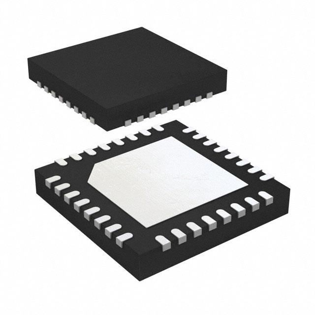
Available in a QFN-32 (5mmx5mm)
Package
Available in AEC-Q100 Grade 1
Internal safety features include configurable
over-current protection (OCP), adjustable dead
time control, under-voltage lockout (UVLO), and
thermal shutdown.
APPLICATIONS
The MPQ6533 is available in a QFN-32
(5mmx5mm) package with an exposed thermal
pad.
All MPS parts are lead-free, halogen-free, and adhere to the RoHS
directive. For MPS green status, please visit the MPS website under Quality
Assurance. “MPS”, the MPS logo, and “Simple, Easy Solutions” are
trademarks of Monolithic Power Systems, Inc. or its subsidiaries.
•
•
Automotive Actuators
Brushed DC Motor Drivers
TYPICAL APPLICATION
VIN
nSLEEP
CP1
CP2
VG
ENA
VRG
VIN
nSCS
SCK
SDI
SDO
nFAULT
BSTA
MPQ6533
GHA
ENB
ENC
SHA
INA
INB
GLA
INC
GND
CSO
AGND
Channel A
(Applicable to
Channels B and C)
MPQ6533 Rev. 1.0
MonolithicPower.com
8/25/2021
MPS Proprietary Information. Patent Protected. Unauthorized Photocopy and Duplication Prohibited.
© 2021 MPS. All Rights Reserved.
1
�MPQ6533 – STEP MOTOR DRIVER W/ INTERNAL CURRENT SENSE, AEC-Q100
ORDERING INFORMATION
Part Number*
MPQ6533GUE-AEC1
Package
QFN-32 (5mmx5mm)
Top Marking
See Below
MSL Rating
3
* For Tape & Reel, add suffix -Z (e.g. MPQ6533GUE-AEC1-Z).
TOP MARKING
MPS: MPS prefix
YY: Year code
WW: Week code
MP6533: Product code of MPQ6533GUE-AEC1
LLLLLLL: Lot number
E: Wettable lead flank
PACKAGE REFERENCE
INB
INA
ENC
ENB
ENA
nSLEEP
nFAULT
CSO
TOP VIEW
AGND
1
24
INC
nSCS
2
23
VRG
SCK
3
22
CP1
SDI
4
21
CP2
SDO
5
20
VIN
BSTA
6
19
VG
SHA
7
18
GND
GHA
8
17
GLC
GHC
SHC
BSTC
GLB
GHB
SHB
BSTB
GLA
GND
QFN-32 (5mmx5mm)
MPQ6533 Rev. 1.0
MonolithicPower.com
8/25/2021
MPS Proprietary Information. Patent Protected. Unauthorized Photocopy and Duplication Prohibited.
© 2021 MPS. All Rights Reserved.
2
�MPQ6533 – STEP MOTOR DRIVER W/ INTERNAL CURRENT SENSE, AEC-Q100
PIN FUNCTIONS
Pin #
Name
Description
18
1
GND
AGND
20
VIN
22
21
CP1
CP2
19
VG
23
6
VRG
BSTA
7
SHA
8
9
10
GHA
GLA
BSTB
11
SHB
12
13
GHB
GLB
Power ground.
Analog ground.
Input supply voltage. Bypass VIN with a minimum 1µF, X7R ceramic capacitor
connected to ground. Additional bulk capacitance may be required.
Reverse battery gate drive charge pump capacitor. Connect a 220nF, X7R ceramic
capacitor between the CP1 and CP2 pins.
Gate drive LDO output voltage. Connect a 10µF, 10V, X7R ceramic capacitor from
VG to ground.
Reverse battery MOSFET gate drive output.
Channel A bootstrap capacitor. Place a ceramic capacitor between BSTA and SHA.
Channel A output (drain of the low-side MOSFET, source of the high-side
MOSFET).
Channel A high-side gate drive output.
Channel A low-side gate drive output.
Channel B bootstrap capacitor. Place a ceramic capacitor between BSTB and SHB.
Channel B output (drain of the low-side MOSFET, source of the high-side
MOSFET).
Channel B high-side gate drive output.
Channel B low-side gate drive output.
13
BSTC
15
SHC
16
17
29
28
29
26
GHC
GLC
ENA
ENB
ENC
INA
25
24
32
INB
INC
CSO
31
nFAULT
5
4
SDO
SDI
3
SCK
2
nSCS
30
nSLEEP
Channel C bootstrap capacitor. Place a ceramic capacitor between BSTC and SHC.
Channel C output (drain of the low-side MOSFET, source of the high-side
MOSFET).
Channel C high-side gate drive output.
Channel C low-side gate drive output.
Channel A enable input. The ENA pin is pulled down internally.
Channel B enable input. The ENB pin is pulled down internally.
Channel C enable input. The ENC pin is pulled down internally.
Channel A input. The INA pin is pulled down internally.
Channel B input. The INB pin is pulled down internally.
Channel C input. The INC pin is pulled down internally.
Current-sense output. The channel is selected by the SPI register
Fault Indication. The nFAULT pin pulls logic low if a fault occurs. nFAULT has an
open-drain output.
Serial data output. SDO has a high impedance when nSCS = 1.
Serial data input. SDI is pulled down internally.
Serial clock input. Data is captured on the rising edge of SCK. SCK is pulled down
internally.
Serial chip selection. The nSCS pin pulls active low to enable serial data transfers.
nSCS is pulled down internally.
Sleep mode input. nSLEEP pulls logic low to enter low-power sleep mode. nSLEEP is
pulled down internally.
MPQ6533 Rev. 1.0
MonolithicPower.com
8/25/2021
MPS Proprietary Information. Patent Protected. Unauthorized Photocopy and Duplication Prohibited.
© 2021 MPS. All Rights Reserved.
3
�MPQ6533 – STEP MOTOR DRIVER W/ INTERNAL CURRENT SENSE, AEC-Q100
θJA
θJC
ABSOLUTE MAXIMUM RATINGS (1)
Thermal Resistance (4)
Input voltage (VIN) ........................ -0.3V to +45V
VRG.............................................. -40V to +59V
VG ……………………………….... -0.3V to +14V
CP1 ……………………………….. -0.3V to +14V
CP1 (transient