MPQ8633B
16V, 20A, Synchronous, Step-Down
Converter with Adjustable Current Limit,
Programmable Frequency, and Voltage Tracking
The Future of Analog IC Technology
DESCRIPTION
The MPQ8633B is a fully integrated, highfrequency, synchronous, buck converter. It
offers a very compact solution that achieves up
to 20A of output current with excellent load and
line regulation over a wide input supply range.
The MPQ8633B operates at high efficiency
over a wide output current load range.
The
MPQ8633B
adopts
an
internally
compensated constant-on-time (COT) control
mode that provides fast transient response and
eases loop stabilization.
The operating frequency can be set to
600kHz, 800kHz, or 1000kHz easily with MODE
configuration,
allowing
the
MPQ8633B
frequency to remain constant regardless of the
input and output voltages.
The output voltage start-up ramp is controlled
by an internal 1ms timer. It can be increased by
adding a capacitor on TRK/REF. An open-drain
power good (PGOOD) signal indicates if the
output is within its nominal voltage range.
PGOOD is clamped at around 0.7V with an
external pull-up voltage when the input supply
fails to power the MPQ8633B.
Full protection features include over-current
protection (OCP), over-voltage protection
(OVP), under-voltage protection (UVP), and
over-temperature protection (OTP).
The MPQ8633B requires a minimal number of
readily
available,
standard,
external
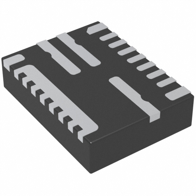
components and is available in a QFN-21
(3mmx4mm) package.
FEATURES
Wide Input Voltage Range
o 2.7V to 16V with External 3.3V VCC
Bias
o 4V to 16V with Internal Bias or External
3.3V VCC Bias
Differential Output Voltage Remote Sense
Programmable Accurate Current Limit Level
20A Output Current
Low RDS(ON) Integrated Power MOSFETs
Proprietary Switching Loss Reduction
Technique
Adaptive COT for Ultrafast Transient
Response
Stable with Zero ESR Output Capacitor
0.5% Reference Voltage over 0°C to +70°C
Junction Temperature Range
1% Reference Voltage from -40°C to
+125°C Junction Temperature Range
Selectable Pulse Skip or Forced CCM
Operation
Excellent Load Regulation
Output Voltage Tracking
Output Voltage Discharge
PGOOD Active Clamped at Low Level
during Power Failure
Programmable Soft-Start Time from 1ms
Pre-Bias Start-Up
Selectable Switching Frequency from
600kHz, 800kHz, and 1000kHz
Non-Latch OCP, UVP, UVLO, Thermal
Shutdown, and Latch-Off for OVP
Output Adjustable from 0.6V to 90%*VIN,
up to 5.5V Max
Available in a QFN-21 (3mmx4mm)
Package
APPLICATIONS
Telecom and Networking Systems
Servers, Cloud-Computing, Storage
Base Stations
General Purpose Point-of-Load (PoL)
12V Distribution Power Systems
High-end TV
Game Consoles and Graphic Cards
All MPS parts are lead-free, halogen-free, and adhere to the RoHS directive.
For MPS green status, please visit the MPS website under Quality
Assurance. “MPS” and “The Future of Analog IC Technology” are registered
trademarks of Monolithic Power Systems, Inc.
MPQ8633B Rev.1.03
www.MonolithicPower.com
11/2/2018
MPS Proprietary Information. Patent Protected. Unauthorized Photocopy and Duplication Prohibited.
© 2018 MPS. All Rights Reserved.
1
�MPQ8633B – 16V, 20A, SYNCHRONOUS, STEP-DOWN CONVERTER W/ ADJUSTABLE
CURRENT LIMIT, PROGRAMMBALE FREQUENCY, AND VOLTAGE TRACKING
TYPICAL APPLICATION
MPQ8633B Rev.1.03
www.MonolithicPower.com
11/2/2018
MPS Proprietary Information. Patent Protected. Unauthorized Photocopy and Duplication Prohibited.
© 2018 MPS. All Rights Reserved.
2
�MPQ8633B – 16V, 20A, SYNCHRONOUS, STEP-DOWN CONVERTER W/ ADJUSTABLE
CURRENT LIMIT, PROGRAMMBALE FREQUENCY, AND VOLTAGE TRACKING
ORDERING INFORMATION
Part Number
MPQ8633BGLE*
Package
QFN-21 (3mmx4mm)
Top Marking
See Below
* For Tape & Reel, add suffix –Z (e.g. MPQ8633BGLE–Z)
TOP MARKING
MP: MPS prefix
Y: Year code
W: Week code
8633B: First five digits of the part number
LLL: Lot number
E: MPQ8633BGLE
PACKAGE REFERENCE
TOP VIEW
QFN-21 (3mmx4mm)
MPQ8633B Rev.1.03
www.MonolithicPower.com
11/2/2018
MPS Proprietary Information. Patent Protected. Unauthorized Photocopy and Duplication Prohibited.
© 2018 MPS. All Rights Reserved.
3
�MPQ8633B – 16V, 20A, SYNCHRONOUS, STEP-DOWN CONVERTER W/ ADJUSTABLE
CURRENT LIMIT, PROGRAMMBALE FREQUENCY, AND VOLTAGE TRACKING
ABSOLUTE MAXIMUM RATINGS (1)
Supply voltage (VIN) ...................................... 18V
VSW(DC) ............................................... -0.3V to VIN
VSW (25ns) (2) ...................................... -3V to 25V
VSW (25ns) .......................................... -5V to 25V
VBST........................................................ VSW + 4V
VCC, EN ........................................................ 4.5V
All other pins .................................. -0.3V to 4.3V
Junction temperature ................................ 170°C
Lead temperature...................................... 260°C
Storage temperature .................-65°C to +170°C
Thermal Resistance (5)
θJB θJC_TOP
QFN-21 (3mmx4mm) ........... 8 ....... 18 ...... °C/W
NOTES:
1) Exceeding these ratings may damage the device.
2) Measured using a differential oscilloscope probe.
3) The device is not guaranteed to function outside of its
operating conditions.
4) The voltage rating can be in the range of -3V to 23V for a
period of 25ns or less with a maximum repetition rate of
1000kHz when the input voltage is 16V.
5) θJB is the thermal resistance from the junction to the board
around the PGND soldering point.
θJC_TOP is the thermal resistance from the junction to the top of
the package.
Recommended Operating Conditions (3)
Supply voltage (VIN) ............................ 4V to 16V
VIN(DC) - VSW(DC) (4) ................... -0.3V to VIN + 0.3V
VSW(DC) (4) ................................ -0.3V to VIN + 0.3V
Output voltage (VOUT) ...................... 0.6V to 5.5V
External VCC bias (VCC_EXT) ......... 3.12V to 3.6V
Maximum output current (IOUT_MAX) ............... 20A
Maximum output current limit (IOC_MAX) ......... 24A
Maximum peak inductor current (IL_PEAK) ...... 28A
EN voltage (VEN) ......................................... 3.6V
Operating junction temp. (TJ). ...-40°C to +125°C
MPQ8633B Rev.1.03
www.MonolithicPower.com
11/2/2018
MPS Proprietary Information. Patent Protected. Unauthorized Photocopy and Duplication Prohibited.
© 2018 MPS. All Rights Reserved.
4
�MPQ8633B – 16V, 20A, SYNCHRONOUS, STEP-DOWN CONVERTER W/ ADJUSTABLE
CURRENT LIMIT, PROGRAMMBALE FREQUENCY, AND VOLTAGE TRACKING
ELECTRICAL CHARACTERISTICS
VIN = 12V, TJ = -40°C to +125°C, unless otherwise noted.
Parameters
Supply Current
Supply current (shutdown)
Supply current (quiescent)
Symbol
IIN
IIN
Condition
Min
Typ
Max
Units
VEN = 0V
VEN = 2V, VFB = 0.62V
0
650
10
850
μA
μA
VEN = 0V, VSW = 0V
VEN = 0V, VSW = 12V
VEN = 2V @ 25oC
VEN = 2V @ 25oC
0
0
8.6
2.5
10
30
μA
1.15
9
1.2
10
-10
200
1.25
11
V
μA/A
A
ns
480
600
720
kHz
680
800
920
kHz
850
1000
1150
kHz
50
180
ns
ns
MOSFET
Switch leakage
HS on-state resistance
LS on-state resistance
Current Limit
Current limit threshold
ICS to IOUT ratio
Low-side negative current limit
Negative current limit time out6)
Switching Frequency
Switching frequency(7)
SWLKG_HS
SWLKG_LS
RDS_ON_HS
RDS_ON_LS
VLIM
ICS/IOUT
ILIM_NEG
tNCL_Timer
fSW
Minimum on time (6)
TON_MIN
(6)
Minimum off time
TOFF_MIN
Over-Voltage and Under-Voltage Protection
OVP threshold
VOVP
UVP threshold
VUVP
Feedback Voltage and Soft Start
Feedback voltage
TRK/REF sourcing current
TRK/REF sinking current
Soft-start time
Error Amplifier
Error amplifier offset
Feedback current
VREF
ITRACK_Source
ITRACK_Sink
tSS
VOS
IFB
IOUT ≥ 2A
MODE = GND, IOUT = 0A,
VOUT = 1V
MODE = 30.1kΩ, IOUT = 0A,
VOUT = 1V
MODE = 60.4 kΩ, IOUT = 0A,
VOUT = 1V
VFB = 500mV
VFB = 500mV
TJ = -40°C to +125°C
TJ = 0°C to +70°C
VTRK/REF = 0V
VTRK/REF = 1V
CTRACK = 1nF, TJ = +25°C
113%
77%
116%
80%
119%
83%
VREF
VREF
594
597
600
600
42
12
1
606
603
1.25
mV
mV
μA
μA
ms
0
50
3
100
mV
nA
0.75
-3
VFB = REF
mΩ
mΩ
MPQ8633B Rev.1.03
www.MonolithicPower.com
11/2/2018
MPS Proprietary Information. Patent Protected. Unauthorized Photocopy and Duplication Prohibited.
© 2018 MPS. All Rights Reserved.
5
�MPQ8633B – 16V, 20A, SYNCHRONOUS, STEP-DOWN CONVERTER W/ ADJUSTABLE
CURRENT LIMIT, PROGRAMMBALE FREQUENCY, AND VOLTAGE TRACKING
ELECTRICAL CHARACTERISTICS (continued)
VIN = 12V, TJ = -40°C to +125°C, unless otherwise noted.
Parameters
Enable and UVLO
Enable input rising threshold
Enable hysteresis
Symbol
VIHEN
VEN-HYS
Enable input current
Soft shutdown discharge FET
VIN UVLO
VIN under-voltage lockout
threshold rising
VIN under-voltage lockout
threshold falling
VCC Regulator
VCC under-voltage lockout
threshold rising
VCC under-voltage lockout
threshold falling
VCC regulator
VCC load regulation
Power Good
Power good high threshold
Power good low threshold
Power good low to high delay
Power good sink current
capability
Power good leakage current
Condition
IEN
Min
Typ
Max
Units
1.17
1.22
200
1.27
V
mV
VEN = 2V
0
RON_DISCH
2.1
VINVth_Rise
μA
80
150
2.4
2.7
VCC = 3.3V
Ω
V
VINvth_Fall
1.55
1.85
2.15
VCCVth_Rise
2.65
2.8
2.95
V
VCCvth_Fall
2.35
2.5
2.65
V
VCC
2.88
3.00
0.5
3.12
V
%
89.5%
113%
77%
0.63
92.5%
116%
80%
0.9
95.5%
119%
83%
1.17
VREF
VREF
VREF
ms
0.5
V
3
µA
650
800
mV
750
900
mV
Icc = 25mA
PGVth_Hi_Rise
PGVth_Lo_Rise
PGVth_Lo_Fall
PGTd
VPG
IPG_LEAK
VOL_100
Power good low-level output
voltage
VOL_10
FB from low to high
FB from low to high
FB from high to low
TJ = 25°C
IPG = 10mA
VPG = 3.3V
VIN = 0V, pull PGOOD up to
3.3V through a 100kΩ
resistor @ 25oC
VIN = 0V, pull PGOOD up to
3.3V through a 10kΩ resistor
@ 25oC
Thermal Protection
Thermal shutdown (6)
Thermal shutdown hysteresis (6)
TSD
160
30
°C
°C
NOTE:
6) Guaranteed by design.
7) Guaranteed by design over temperature.
MPQ8633B Rev.1.03
www.MonolithicPower.com
11/2/2018
MPS Proprietary Information. Patent Protected. Unauthorized Photocopy and Duplication Prohibited.
© 2018 MPS. All Rights Reserved.
6
�MPQ8633B – 16V, 20A, SYNCHRONOUS, STEP-DOWN CONVERTER W/ ADJUSTABLE
CURRENT LIMIT, PROGRAMMBALE FREQUENCY, AND VOLTAGE TRACKING
TYPICAL PERFORMANCE CHARACTERISTICS
VIN = 12V, TA = 25˚C, VOUT = 1V, FS = 800kHz unless otherwise noted.
, No Air-Flow
100
100
110
95
95
100
90
90
90
85
85
80
80
80
70
75
75
60
70
70
50
65
Vo=5V
Vo=5V
65
60
Vo=2.5V
60
Vo=2.5V
55
Vo=1V
55
Vo=1V
50
0
5
10
15
20
50
40
5
10
15
Vo=2.5V
20
10
0
Vo=5V
30
20
Vo=1V
0
2
4
6 8 10 12 14 16 18 20
Switching Frequency
vs. Input Voltage
Forced CCM
1.012
600KHz
1300
VOUT=1V, 3A Load
1200
1000KHz
FREQUENCY (kHz)
800KHz
1.011
1.010
1.009
Forced CCM
1100
1000
900
600kHz
800kHz
1MHz
800
700
Pulse Skip
0
2
4
6
8 10 12 14 16 18 20
1.008
0
5
10
15
20
600
4
6
8
10
12
14
INPUT VOLTAGE (V)
16
Switching Frequency
vs. Output Voltage
V =12V, 3A Load
1300 IN
FREQUENCY (kHz)
1200
1100
1000
900
600kHz
800kHz
1MHz
800
700
600
1
1.5 2 2.5 3 3.5 4 4.5
OUTPUT VOLTAGE (V)
5
MPQ8633B Rev.1.03
www.MonolithicPower.com
11/2/2018
MPS Proprietary Information. Patent Protected. Unauthorized Photocopy and Duplication Prohibited.
© 2018 MPS. All Rights Reserved.
7
�MPQ8633B – 16V, 20A, SYNCHRONOUS, STEP-DOWN CONVERTER W/ ADJUSTABLE
CURRENT LIMIT, PROGRAMMBALE FREQUENCY, AND VOLTAGE TRACKING
TYPICAL PERFORMANCE CHARACTERISTICS (continued)
VIN = 12V, TA = 25˚C, VOUT = 1V, FS = 800kHz unless otherwise noted.
Steady State
Steady State
Steady State
IOUT = 0A, Pulse Skip
IOUT = 0.5A, Pulse Skip
IOUT = 20A, Pulse Skip
VSW
5V/div.
VSW
5V/div.
VSW
5V/div.
VOUT/AC
10mV/div.
VOUT/AC
20mV/div.
VOUT/AC
10mV/div.
Steady State
Steady State
Load Transient
IOUT = 0A, Forced CCM
IOUT = 20A, Forced CCM
IOUT =0A~8A, Pulse Skip
VOUT/AC
50mV/div.
VSW
5V/div.
VSW
5V/div.
VOUT/AC
20mV/div.
VOUT/AC
20mV/div.
VSW
5V/div.
IL
10A/div.
VOUT/AC
50mV/div.
VSW
5V/div.
IL
10A/div.
Load Transient
Power Up through EN
Power Up through EN
IOUT=0A~8A, Forced CCM
IOUT = 0A, Pulse Skip
IOUT = 20A, Pulse Skip
VEN
2V/div.
VEN
2V/div.
VOUT
500mV/div.
VOUT
500mV/div.
IL
10A/div.
IL
10A/div.
VPGOOD
2V/div.
VPGOOD
2V/div.
MPQ8633B Rev.1.03
www.MonolithicPower.com
11/2/2018
MPS Proprietary Information. Patent Protected. Unauthorized Photocopy and Duplication Prohibited.
© 2018 MPS. All Rights Reserved.
8
�MPQ8633B – 16V, 20A, SYNCHRONOUS, STEP-DOWN CONVERTER W/ ADJUSTABLE
CURRENT LIMIT, PROGRAMMBALE FREQUENCY, AND VOLTAGE TRACKING
TYPICAL PERFORMANCE CHARACTERISTICS (continued)
VIN = 12V, TA = 25˚C, VOUT = 1V, FS = 800kHz unless otherwise noted.
Power Up through EN
Power Up through EN
Power Down through EN
IOUT = 0A, Forced CCM
IOUT = 20A, Forced CCM
IOUT=0A, Pulse Skip
VEN
2V/div.
VEN
2V/div.
VEN
2V/div.
VOUT
500mV/div.
VOUT
500mV/div.
VOUT
500mV/div.
IL
10A/div.
IL
10A/div.
IL
10A/div.
VPGOOD
2V/div.
VPGOOD
2V/div.
VPGOOD
2V/div.
Power Down through EN
Power Down through EN
Power Down through EN
IOUT=20A, Pulse Skip
IOUT=0A, Forced CCM
IOUT=20A, Forced CCM
VEN
2V/div.
VEN
2V/div.
VEN
2V/div.
VOUT
500mV/div.
VOUT
500mV/div.
VOUT
500mV/div.
IL
10A/div.
IL
10A/div.
IL
10A/div.
VPGOOD
2V/div.
VPGOOD
2V/div.
VPGOOD
2V/div.
Pre-bias Start-Up
Pre-bias Start-Up
Over-Current
Pulse skip
Forced CCM
Protection Entry
VEN
2V/div.
VEN
2V/div.
VOUT
500mV/div.
VOUT
500mV/div.
VSW
5V/div.
VSW
5V/div.
VPGOOD
2V/div.
VPGOOD
2V/div.
VOUT
500mV/div.
VTRK/REF
500mV/div.
IL
10A/div.
MPQ8633B Rev.1.03
www.MonolithicPower.com
11/2/2018
MPS Proprietary Information. Patent Protected. Unauthorized Photocopy and Duplication Prohibited.
© 2018 MPS. All Rights Reserved.
9
�MPQ8633B – 16V, 20A, SYNCHRONOUS, STEP-DOWN CONVERTER W/ ADJUSTABLE
CURRENT LIMIT, PROGRAMMBALE FREQUENCY, AND VOLTAGE TRACKING
TYPICAL PERFORMANCE CHARACTERISTICS (continued)
VIN = 12V, TA = 25˚C, VOUT = 1V, FS = 800kHz unless otherwise noted.
IL
2A/div.
VPGOOD
1V/div.
VOUT
500mV/div.
VTRK/REF
500mV/div.
IL
10A/div.
IL
5A/div.
VOUT
500mV/div.
VSW
5V/div.
VOUT
500mV/div.
VPGOOD
1V/div.
IL
5A/div.
VOUT
500mV/div.
MPQ8633B Rev.1.03
www.MonolithicPower.com
11/2/2018
MPS Proprietary Information. Patent Protected. Unauthorized Photocopy and Duplication Prohibited.
© 2018 MPS. All Rights Reserved.
10
�MPQ8633B – 16V, 20A, SYNCHRONOUS, STEP-DOWN CONVERTER W/ ADJUSTABLE
CURRENT LIMIT, PROGRAMMBALE FREQUENCY, AND VOLTAGE TRACKING
PIN FUNCTIONS
QFN-21
PIN #
Name
1
BST
2
AGND
3
CS
4
MODE
5
TRK/REF
6
RGND
7
FB
8
EN
9
PGOOD
10, 21
VIN
11-18
PGND
19
VCC
20
SW
Description
Bootstrap. Connect a capacitor between SW and BS to form a floating supply
across the high-side switch driver.
Analog ground. Select AGND as the control circuit reference point.
Current limit. Connect a resistor to AGND to set the current limit trip point. See
equation 4 for additional details.
Operation mode selection. Program MODE to select CCM, pulse skip mode, and
the operating switching frequency. See Table 1 for additional details.
External tracking voltage input. The output voltage tracks this input signal.
Decouple TRK/REF with a ceramic capacitor placed as close to it as possible. X7R
or X5R grade dielectric ceramic capacitors are recommended for their stable
temperature characteristics. The capacitance of this capacitor determines the softstart time. See Equation 2 and 3 for additional details.
Differential remote sense negative input. Connect RGND to the negative side of
the voltage sense point directly. Short RGND to GND if the remote sense is not
used.
Feedback (differential remote sense positive input). An external resistor divider
from the output to RGND tapped to FB sets the output voltage. It is recommended
to place the resistor divider as close to FB as possible. Vias should be avoided on
the FB traces.
Enable. EN is an input signal that turns the regulator on or off. Drive EN high to turn
on the regulator; drive EN low to turn off the regulator. Connect EN to VIN through a
pull-up resistor or a resistive voltage divider for automatic start-up. Do not float EN.
Power good output. PGOOD is an open-drain signal. A pull-up resistor connected
to a DC voltage is required to indicate a logic high signal if the output voltage is
within regulation. There is a delay of about 1ms between the time FB ≥ 92.5% and
PGOOD pulling high.
Input voltage. VIN supplies power for the internal MOSFET and regulator. Input
capacitors are needed to decouple the input rail. Use wide PCB traces to make the
connection.
System ground. PGND is the reference ground of the regulated output voltage.
Therefore, care must be taken during PCB layout. Use wide PCB traces to make
the connection.
Internal 3V LDO output. The driver and control circuits are powered from the VCC
voltage. Decouple VCC with a ceramic capacitor at least 1µF placed as close to it
as possible. X7R or X5R grade dielectric ceramic capacitors are recommended for
their stable temperature characteristics.
Switch output. Connect SW to the inductor and bootstrap capacitor. SW is driven
up to VIN by the high-side switch during the on-time of the PWM duty cycle. The
inductor current drives SW low during the off-time. Use wide PCB traces to make
the connection.
MPQ8633B Rev.1.03
www.MonolithicPower.com
11/2/2018
MPS Proprietary Information. Patent Protected. Unauthorized Photocopy and Duplication Prohibited.
© 2018 MPS. All Rights Reserved.
11
�MPQ8633B – 16V, 20A, SYNCHRONOUS, STEP-DOWN CONVERTER W/ ADJUSTABLE
CURRENT LIMIT, PROGRAMMBALE FREQUENCY, AND VOLTAGE TRACKING
BLOCK DIAGRAM
Figure 1: Functional Block Diagram
MPQ8633B Rev.1.03
www.MonolithicPower.com
11/2/2018
MPS Proprietary Information. Patent Protected. Unauthorized Photocopy and Duplication Prohibited.
© 2018 MPS. All Rights Reserved.
12
�MPQ8633B – 16V, 20A, SYNCHRONOUS, STEP-DOWN CONVERTER W/ ADJUSTABLE
CURRENT LIMIT, PROGRAMMBALE FREQUENCY, AND VOLTAGE TRACKING
OPERATION
COT Control
The MPQ8633B employs a constant-on-time
(COT) control to achieve a fast load transient
response. Figure 2 shows the details of the
control stage of the MPQ8633B.
The operational amplifier (AMP) corrects any
error voltage between FB and VREF. The
MPQ8633B can use AMP to provide excellent
load regulation over the entire load range in
either forced continuous conduction mode
(CCM) or pulse skip mode.
MOSFET (LS-FET) turns on when the HS-FET
is in its off state to minimize conduction loss. A
dead short occurs between VIN and PGND if
both the HS-FET and the LS-FET are turned on
at the same time. This is called a shoot-through.
To avoid a shoot-through, a dead time (DT) is
generated internally between the HS-FET off
and the LS-FET on period or the LS-FET off
and the HS-FET on period.
The dedicated RGND pin helps provide the
feature of the differential output voltage remote
sense. The pair of the remote sense trace
should be kept in low impedance to achieve the
best performance.
The MPQ8633B has an internal RAMP
compensation to support a low ESR MLCC
output capacitor solution. The adaptive internal
RAMP is optimized so that the MPQ8633B is
stable in the entire operating input and output
voltage ranges with a proper design of the
output L/C filter.
Figure 3: Heavy-Load Operation (PWM)
Figure 2: COT Control
PWM Operation
Figure 3 shows how the PWM signal is
generated. AMP corrects any error between FB
and REF and generates a fairly smooth DC
voltage (COMP). The internal RAMP is
superimposed onto COMP, which is compared
with the FB signal. Whenever FB drops below
the superimposed COMP, the integrated highside MOSFET (HS-FET) is turned on. The HSFET remains on for a fixed turn-on time. The
fixed on time is determined by the input voltage,
output voltage, and selected switching
frequency. After the on period elapses, the HSFET turns off. It turns on again when FB drops
below the superimposed COMP. By repeating
this operation, the MPQ8633B regulates the
output voltage. The integrated low-side
CCM Operation
Continuous conduction mode (CCM) occurs
when the output current is high, and the
inductor current is always above zero amps
(see Figure 3). The MPQ8633B can also be
configured to operate in forced CCM operation
when the output current is low (see the Mode
Selection section on page 14 for details).
In CCM operation, the switching frequency is
fairly constant (PWM mode), hence the output
ripple remains almost constant throughout the
entire load range.
Pulse Skip Operation
In light-load condition, the MPQ8633B can be
configured to work in pulse skip mode to
optimize efficiency. When the load decreases,
the inductor current decreases as well. Once
the inductor current reaches zero, the
MPQ8633B transitions from CCM to pulse skip
mode if the MPQ8633B is configured in this
MPQ8633B Rev.1.03
www.MonolithicPower.com
11/2/2018
MPS Proprietary Information. Patent Protected. Unauthorized Photocopy and Duplication Prohibited.
© 2018 MPS. All Rights Reserved.
13
�MPQ8633B – 16V, 20A, SYNCHRONOUS, STEP-DOWN CONVERTER W/ ADJUSTABLE
CURRENT LIMIT, PROGRAMMBALE FREQUENCY, AND VOLTAGE TRACKING
way (see the Mode Selection section on page
14 for details).
Figure 4 shows pulse skip mode operation at
light-load condition. When FB drops below the
superimposed COMP, the HS-FET turns on for
a fixed interval. When the HS-FET turns off, the
LS-FET turns on until the inductor current
reaches zero. In pulse skip mode operation, FB
does not reach superimposed COMP when the
inductor current approaches zero. The LS-FET
driver turns into tri-state (high-Z) when the
inductor current reaches zero. A current
modulator takes over the control of the LS-FET
and limits the inductor current to less than
-1mA. Therefore, the output capacitors
discharge slowly to PGND through the LS-FET.
At light-load condition, the HS-FET is not turned
on as frequently in pulse skip mode as it is in
forced CCM. As a result, the efficiency in pulse
skip mode is improved greatly compared to that
in forced CCM operation.
IOUT
( VIN VOUT ) VOUT
2 L FSW VIN
(1)
Where FSW is the switching frequency.
The MPQ8633B enters PWM mode once the
output current exceeds the critical level.
Afterward, the switching frequency remains
fairly constant over the output current range.
The MPQ8633B can be configured to operate in
forced CCM, even in light-load condition (see
Table 1).
Mode Selection
The MPQ8633B provides both forced CCM
operation and pulse skip mode operation in
light-load condition. The MPQ8633B has three
options for switching frequency selection.
Selecting the operation mode under light-load
condition and the switching frequency is done
by choosing the resistance value of the resistor
connected between MODE and AGND or VCC
(see Table 1).
Table 1: MODE Selection
MODE
VCC
243kΩ (±20%)
to GND
121kΩ (±20%)
to GND
GND
30.1kΩ (±20%)
to GND
60.4kΩ (±20%)
to GND
Figure 4: Pulse Skip in Light Load
As the output current increases from light load,
the time period the current modulator regulates
in becomes shorter. The HS-FET is turned on
more frequently, and the switching frequency
increases accordingly. The output current
reaches critical levels when the current
modulator time is zero. The critical level of the
output current can be determined with Equation
(1):
Light-Load
Mode
Pulse skip
Switching
Frequency
600kHz
Pulse skip
800kHz
Pulse skip
1000kHz
Forced CCM
600kHz
Forced CCM
800kHz
Forced CCM
1000kHz
Soft Start (SS)
The minimum soft-start time is limited at 1ms. It
can be increased by adding a SS capacitor
between TRK/REF and RGND.
The total SS capacitor value can be determined
with Equation (2) and (3):
CSS (nF)
t ss (ms) 36A
0.6(V)
CSS CSS1 CSS2
(2)
(3)
where CSS2 is recommended to be minimum of
22nF.
MPQ8633B Rev.1.03
www.MonolithicPower.com
11/2/2018
MPS Proprietary Information. Patent Protected. Unauthorized Photocopy and Duplication Prohibited.
© 2018 MPS. All Rights Reserved.
14
�MPQ8633B – 16V, 20A, SYNCHRONOUS, STEP-DOWN CONVERTER W/ ADJUSTABLE
CURRENT LIMIT, PROGRAMMBALE FREQUENCY, AND VOLTAGE TRACKING
Output Voltage Tracking and Reference
The MPQ8633B provides an analog input pin
(TRK/REF) to track another power supply or
accept an external reference. When an external
voltage signal is connected to TRK/REF, it acts
as a reference for the MPQ8633B output
voltage. The FB voltage follows this external
voltage signal exactly, and the soft-start
settings are ignored. The TRK/REF input signal
can be in the range of 0.3V to 1.4V. During the
initial start-up, the TRK/REF must reach at least
600mV first to ensure proper operation. After
that, it can be set to any value between 0.3V
and 1.4V.
Pre-Bias Start-Up
The MPQ8633B is designed for monotonic
start-up into pre-biased loads. If the output is
pre-biased to a certain voltage during start-up,
the IC disables switching for both the HS-FET
and LS-FET until the voltage on the TRK/REF
capacitor exceeds the sensed output voltage at
FB. Before the TRK/REF voltage reaches the
pre-biased FB level, if the BST voltage (from
BST to SW) is lower than 2.3V, the LS-FET is
turned on to allow the BST voltage to be
charged through VCC. The LS-FET is turned on
for very narrow pulses, so the drop in the prebiased level is negligible.
Output Voltage Discharge
When the MPQ8633B is disabled through EN,
output voltage discharge mode is enabled. This
causes both the HS-FET and the LS-FET to
latch off. A discharge FET connected between
SW and PGND is turned on to discharge the
output voltage. The typical switch on resistance
of this FET is about 80Ω. Once the FB voltage
drops below 10%*REF, the discharge FET is
turned off.
Current Sense and Over-Current Protection
(OCP)
The MPQ8633B features an on-die current
sense and a programmable positive current
limit threshold.
The current limit is active when the MPQ8633B
is enabled. During the LS-FET on state, the SW
current (inductor current) is sensed and
mirrored to CS with the ratio of GCS. By using a
resistor (RCS) from CS to AGND, the VCS
voltage is proportional to the SW current cycleby-cycle. The HS-FET is only allowed to turn on
when VCS is below the internal OCP voltage
threshold (VOCP) during the LS-FET on state to
limit the SW valley current cycle-by-cycle.
Calculate the current limit threshold setting from
RCS with Equation (4):
RCS ()
GCS (ILIM
VOCP
(V VO ) VO
1
IN
)
VIN
2 L fs
(4)
Where VOCP = 1.2V, GCS = 10µA/A, and ILIM is
the desired output current limit (A).
The OCP hiccup is active 3ms after the
MPQ8633B is enabled. Once OCP hiccup is
active, if the MPQ8633B detects the overcurrent condition for 31 consecutive cycles, or if
FB drops below the under-voltage protection
(UVP) threshold, it enters hiccup mode. In
hiccup mode, the MPQ8633B latches off the
HS-FET immediately, and latches off the LSFET after ZCD is detected. Meanwhile, the
TRK/REF capacitor is also discharged. After
about 11ms, the MPQ8633B attempts to soft
start automatically. If the over-current condition
still remains after 3ms of running, the
MPQ8633B repeats this operation cycle until
the over-current condition disappears, and the
output voltage rises back to the regulation level
smoothly.
Negative Inductor Current Limit
When the LS-FET detects a -10A current, the
MPQ8633B turns off the LS-FET for 200ns to
limit the negative current.
Output Sinking Mode (OSM)
The MPQ8633B employs output sinking mode
(OSM) to regulate the output voltage to the
targeted value. When the FB voltage is higher
than 104%*REF but is below the OVP threshold,
OSM is triggered. During OSM operation, the
LS-FET remains on until it reaches the -9A
current limit. The LS-FET is then turned off
momentarily for 200ns before turning on again.
The MPQ8633B repeats this operation until FB
drops below 102%*REF. The MPQ8633B exits
OSM after 15 consecutive cycles of forced
CCM.
MPQ8633B Rev.1.03
www.MonolithicPower.com
11/2/2018
MPS Proprietary Information. Patent Protected. Unauthorized Photocopy and Duplication Prohibited.
© 2018 MPS. All Rights Reserved.
15
�MPQ8633B – 16V, 20A, SYNCHRONOUS, STEP-DOWN CONVERTER W/ ADJUSTABLE
CURRENT LIMIT, PROGRAMMBALE FREQUENCY, AND VOLTAGE TRACKING
Over-Voltage Protection (OVP)
The MPQ8633B monitors the output voltage by
connecting FB to the tap of the output voltage
feedback resistor divider to detect an overvoltage condition. This provides latch-off OVP
mode.
Output Voltage Setting and Remote Output
Voltage Sensing
First, choose a value for RFB1. Then RFB2 can be
determined with Equation (5):
If the FB voltage exceeds 116% of the REF
voltage, the MPQ8633B enters latch-off OVP
mode. The HS-FET latches off and PGOOD
latches low until VCC or EN is recycled (turned
off and turned on again). Meanwhile, the LSFET remains on until it reaches the low-side
negative current limit (NOCP). The LS-FET is
then turned off momentarily for 200ns before
turning on again. The MPQ8633B repeats this
operation to attempt to bring down the output
voltage. When the FB voltage drops below 50%
of the REF voltage, the LS-FET is turned off for
pulse skip mode and continues turning on for
forced CCM operation. If FB rises higher than
116% of the REF voltage again, the LS-FET
turns on again with NOCP until FB drops back
below 50% of the REF voltage. The MPQ8633B
needs EN or VIN to recycle to clear the OVP
fault.
(5)
The OVP function is enabled after TRK/REF
reaches 600mV.
Over-Temperature Protection (OTP)
The
MPQ8633B
has
over-temperature
protection (OTP). The IC monitors the junction
temperature
internally.
If
the
junction
temperature exceeds the threshold value
(typically 160°C), the converter shuts off and
discharges the TRK/REF capacitors. This is a
non-latch protection. There is a hysteresis of
about 30°C. Once the junction temperature
drops to about 130°C, a soft start is initiated.
The OTP function is effective once the
MPQ8633B is enabled.
RFB2 (k )
VREF
RFB1(k )
VO VREF
To optimize the load transient response, a feedforward capacitor (CFF) is recommended to be
placed in parallel with RFB1. RFB1 and CFF add an
extra zero to the system, which improves loop
response. RFB1 and CFF are selected so that the
zero formed by RFB1 and CFF is located around
20kHz~60kHz. Calculate this zero with
Equation (6):
fZ
1
2 RFB1 CFF
(6)
Power Good (PGOOD)
The MPQ8633B has a power good (PGOOD)
output. PGOOD is the open-drain of a MOSFET.
Connect PGOOD to VCC or another external
voltage source less than 3.6V through a pull-up
resistor (typically 10kΩ). After applying the input
voltage, the MOSFET turns on, so PGOOD is
pulled to GND before TRK/REF is ready. After
the FB voltage reaches 92.5% of the REF
voltage, PGOOD is pulled high after a 0.8ms
delay.
When the FB voltage drops to 80% of the REF
voltage, or exceeds 116% of the nominal REF
voltage, PGOOD is latched low. PGOOD can
only be pulled high again after a new SS.
If the input supply fails to power the MPQ8633B,
PGOOD is clamped low, even though PGOOD
is tied to an external DC source through a pullup resistor. The relationship between the
PGOOD voltage and the pull-up current is
shown in Figure 5.
MPQ8633B Rev.1.03
www.MonolithicPower.com
11/2/2018
MPS Proprietary Information. Patent Protected. Unauthorized Photocopy and Duplication Prohibited.
© 2018 MPS. All Rights Reserved.
16
�MPQ8633B – 16V, 20A, SYNCHRONOUS, STEP-DOWN CONVERTER W/ ADJUSTABLE
CURRENT LIMIT, PROGRAMMBALE FREQUENCY, AND VOLTAGE TRACKING
The MPQ8633B provides accurate EN
thresholds, so a resistor divider from VIN to
AGND can be used to program the input
voltage, at which the MPQ8633B is enabled.
This is highly recommended for applications
where there is no dedicated EN control logic
signal to avoid possible UVLO bouncing during
power-up and power-down. The resistor divider
values can be determined with Equation (7):
2
1.8
1.6
I_PG( mA)
1.4
1.2
1
0.8
0.6
0.4
VIN _ START ( V ) VIHEN
0.2
0
0.6
0.7
0.8
0.9
V_PG(V)
Figure 5: PGOOD Clamped Voltage vs. Pull-Up
Current
Enable (EN) Configuration
The MPQ8633B turns on when EN goes high;
the MPQ8633B turns off when EN goes low. EN
cannot be left floating for proper operation. EN
can be driven by an analog or digital control
logic signal to enable or disable the MPQ8633B.
R UP R DOWN
R DOWN
(7)
Where VIHEN is 1.22V, typically.
RUP and RDOWN should be chosen so that VEN
does not exceed 3.6V when VIN reaches the
maximum value.
EN can also be connected to VIN directly
through a pull-up resistor (RUP). RUP should be
chosen so that the maximum current going to
EN is 50μA. RUP can be calculated with
Equation (8):
RUP (KΩ)
VINMAX (V)
0.05(mA)
MPQ8633B Rev.1.03
www.MonolithicPower.com
11/2/2018
MPS Proprietary Information. Patent Protected. Unauthorized Photocopy and Duplication Prohibited.
© 2018 MPS. All Rights Reserved.
(8)
17
�MPQ8633B – 16V, 20A, SYNCHRONOUS, STEP-DOWN CONVERTER W/ ADJUSTABLE
CURRENT LIMIT, PROGRAMMBALE FREQUENCY, AND VOLTAGE TRACKING
APPLICATION INFORMATION
Input Capacitor
The input current to the step-down converter is
discontinuous and therefore requires a
capacitor to supply AC current to the step-down
converter while maintaining the DC input
voltage. Use ceramic capacitors for the best
performance. During layout, place the input
capacitors as close to VIN as possible.
The capacitance can vary significantly with
temperature. Capacitors with X5R and X7R
ceramic dielectrics are recommended because
they are fairly stable over a wide temperature
range and offer very low ESR.
The capacitors must have a ripple current rating
that exceeds the converter’s maximum input
ripple current. Estimate the input ripple current
with Equation (9):
ICIN IOUT
VOUT
V
(1 OUT )
VIN
VIN
(9)
The worst-case condition occurs at VIN = 2VOUT,
shown in Equation (10):
ICIN
IOUT
2
(10)
For simplification, choose an input capacitor
with an RMS current rating that exceeds half
the maximum load current. The input capacitor
value determines the converter input voltage
ripple. If there is an input voltage ripple
requirement in the system, select an input
capacitor that meets the specification.
Estimate the input voltage ripple with Equation
(11):
IOUT
V
V
VIN
OUT (1 OUT )
FSW CIN
VIN
VIN
VOUT
VOUT
V
1
)
(1 OUT ) (RESR
FSW L
VIN
8 FSW COUT
(11)
(12)
(13)
When
using
ceramic
capacitors,
the
capacitance dominates the impedance at the
switching frequency. The capacitance also
dominates the output voltage ripple. For
simplification, estimate the output voltage ripple
with Equation (14):
VOUT
VOUT
2
8 FSW L COUT
(1
VOUT
) (14)
VIN
For simplification, the output ripple can be
approximated with Equation (15):
VOUT
VOUT
V
(1 OUT ) RESR
FSW L
VIN
(15)
Inductor
The inductor supplies a constant current to the
output load while being driven by the switching
input voltage. A larger value inductor results in
less ripple current and lower output ripple
voltage, but also has a larger physical size, a
higher series resistance, and a lower saturation
current. Generally, select an inductor value that
allows the inductor peak-to-peak ripple current
to be 30% to 40% of the maximum switch
current limit. Also design for a peak inductor
current that is below the maximum switch
current limit. Calculate the inductance value
with Equation (16):
L
The worst-case condition occurs at VIN = 2VOUT,
where:
IOUT
1
VIN
4 FSW CIN
Output Capacitor
The output capacitor maintains the DC output
voltage. Use POSCAP or ceramic capacitors.
Estimate the output voltage ripple with Equation
(13):
VOUT
V
(1 OUT )
FSW IL
VIN
(16)
Where ∆IL is the peak-to-peak inductor ripple
current.
Choose an inductor that will not saturate under
the maximum inductor peak current. The peak
inductor current can be calculated with
Equation (17):
ILP IOUT
VOUT
V
(1 OUT )
2 FSW L
VIN
MPQ8633B Rev.1.03
www.MonolithicPower.com
11/2/2018
MPS Proprietary Information. Patent Protected. Unauthorized Photocopy and Duplication Prohibited.
© 2018 MPS. All Rights Reserved.
(17)
18
�MPQ8633B – 16V, 20A, SYNCHRONOUS, STEP-DOWN CONVERTER W/ ADJUSTABLE
CURRENT LIMIT, PROGRAMMBALE FREQUENCY, AND VOLTAGE TRACKING
PCB Layout Guidelines
Efficient PCB layout is critical for stable
operation. For best performance, refer to Figure
6 and follow the guidelines below.
5. Place the VCC decoupling capacitor close
to the device.
1. Place the input MLCC capacitors as close to
VIN and PGND as possible.
2. Place the major MLCC capacitors on the
same layer as the MPQ8633B.
7. Place the BST capacitor as close to BST
and SW as possible with 20 mil or wider
traces to route the path. It is recommended
to use a bootstrap capacitor 0.1µF to 1µF.
3. Maximize the VIN and PGND copper plane
to minimize the parasitic impedance.
8. Place the REF capacitor close to TRK/REF
to RGND.
4. Place as many PGND vias as possible as
close to PGND as possible to minimize both
parasitic impedance and thermal resistance.
9. Place via at least 10mm away from the
positive side of the first input decoupling
capacitor close to the IC if it must be placed
on the PGOOD pad.
6. Connect AGND and PGND at the point of
the VCC capacitor's ground connection.
10. Place the OSENSE capacitor in between
the output sense lines and close to the
device.
Cosense
VOSENSE+
VOSENSE-
RFB1
CFF
CSS2 V O
CSS1
RCS
RFB2
MODE
CS
AGND
BST
5
4
3
2
1
15
16
17
18
19
PGND
PGND
PGND
PGND
PGND
CIN3
PGND
REF/TRK
PGND
PGND
14
12
13
11
6
8
7
EN
9
FB
PGOOD
RGND
RBST
21
VIN
20
SW
10
VIN
CIN2
CIN1
VCC
CVCC
Figure 6: Recommended PCB Layout
MPQ8633B Rev.1.03
www.MonolithicPower.com
11/2/2018
MPS Proprietary Information. Patent Protected. Unauthorized Photocopy and Duplication Prohibited.
© 2018 MPS. All Rights Reserved.
19
�MPQ8633B – 16V, 20A, SYNCHRONOUS, STEP-DOWN CONVERTER W/ ADJUSTABLE
CURRENT LIMIT, PROGRAMMBALE FREQUENCY, AND VOLTAGE TRACKING
PACKAGE INFORMATION
QFN-21 (3mmx4mm)
PIN 1 ID
0.15 X 45° TYP
PIN 1 ID
MARKING
PIN 1 ID
INDEX AREA
BOTTOM VIEW
TOP VIEW
SIDE VIEW
0.15 X 45°
NOTE:
1) LAND PATTERN OF PIN1,9,10,11,19,20 AND
21 HAVE THE SAME WIDTH.
2) ALL DIMENSIONS ARE IN MILLIMETERS.
3) EXPOSED PADDLE SIZE DOES NOT INCLUDE
MOLD FLASH.
4) LEAD COPLANARITY SHALL BE 0.10
MILLIMETERS MAX.
5) JEDEC REFERENCE IS MO-220.
6) DRAWING IS NOT TO SCALE.
RECOMMENDED LAND PATTERN
NOTICE: The information in this document is subject to change without notice. Users should warrant and guarantee that third
party Intellectual Property rights are not infringed upon when integrating MPS products into any application. MPS will not
assume any legal responsibility for any said applications.
MPQ8633B Rev. 1.03
www.MonolithicPower.com
11/2/2018
MPS Proprietary Information. Patent Protected. Unauthorized Photocopy and Duplication Prohibited.
© 2018 MPS. All Rights Reserved.
20
�