BDV65B�(NPN),
BDV64B�(PNP)
Complementary Silicon
Plastic Power Darlingtons
. . . for use as output devices in complementary general purpose
amplifier applications.
Features
• High DC Current Gain − HFE = 1000 (min) @ 5 Adc
• Monolithic Construction with Built−in Base Emitter Shunt Resistors
• These are Pb−Free Devices*
MAXIMUM RATINGS
Rating
Collector−Emitter Voltage
Symbol
Max
Unit
http://onsemi.com
10 AMPERE DARLINGTON
COMPLEMENTARY SILICON
POWER TRANSISTORS
60−80−100−120 VOLTS,
125 WATTS
VCEO
100
Vdc
NPN
Collector−Base Voltage
VCB
100
Vdc
COLLECTOR 2
Emitter−Base Voltage
VEB
5.0
Vdc
IC
10
20
Adc
Collector Current
− Continuous
− Peak
Base Current
IB
0.5
Adc
Total Device Dissipation @ TC = 25°C
Derate above 25°C
PD
125
1.0
W
W/°C
TJ, Tstg
-65 to
+�150
°C
Symbol
Max
Unit
RqJC
1.0
°C/W
Operating and Storage Junction Temperature
Range
BASE
1
BASE
1
EMITTER 3
BDV65B
THERMAL CHARACTERISTICS
Characteristic
Thermal Resistance, Junction−to−Case
Stresses exceeding Maximum Ratings may damage the device. Maximum
Ratings are stress ratings only. Functional operation above the Recommended
Operating Conditions is not implied. Extended exposure to stresses above the
Recommended Operating Conditions may affect device reliability.
*For additional information on our Pb−Free strategy and soldering details, please
download the ON Semiconductor Soldering and Mounting Techniques
Reference Manual, SOLDERRM/D.
PNP
COLLECTOR 2,4
EMITTER 3
BDV64B
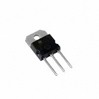
SOT−93
(TO−218)
CASE 340D
1
2
3
TO−247
CASE 340L
STYLE 3
NOTE: Effective June 2012 this device will
be available only in the TO−247
package. Reference FPCN# 16827.
ORDERING INFORMATION
See detailed ordering and shipping information in the package
dimensions section on page 2 of this data sheet.
© Semiconductor Components Industries, LLC, 2012
May, 2012 − Rev. 14
1
Publication Order Number:
BDV65B/D
�BDV65B (NPN), BDV64B (PNP)
MARKING DIAGRAMS
TO−247
TO−218
BDV6xB
AYWWG
1 BASE
AYWWG
BDV6xB
3 EMITTER
1 BASE
2 COLLECTOR
BDV6xB
A
Y
WW
G
3 EMITTER
2 COLLECTOR
= Device Code
x = 4 or 5
= Assembly Location
= Year
= Work Week
= Pb−Free Package
ORDERING INFORMATION
Device Order Number
Package Type
Shipping
BDV65BG
TO−218
(Pb−Free)
30 Units / Rail
BDV64BG
TO−218
(Pb−Free)
30 Units / Rail
BDV65BG
TO−247
(Pb−Free)
30 Units / Rail
BDV64BG
TO−247
(Pb−Free)
30 Units / Rail
1.0
DERATING FACTOR
0.8
0.6
0.4
0.2
0
0
25
50
100
75
TC, CASE TEMPERATURE (°C)
Figure 1. Power Derating
http://onsemi.com
2
125
150
�BDV65B (NPN), BDV64B (PNP)
ÎÎÎÎÎÎÎÎÎÎÎÎÎÎÎÎÎÎÎÎÎÎÎÎÎÎÎÎÎÎÎÎÎ
ÎÎÎÎÎÎÎÎÎÎÎÎÎÎÎÎÎÎÎÎÎÎÎÎÎÎÎÎÎÎÎÎÎ
ÎÎÎÎÎÎÎÎÎÎÎÎÎÎÎÎÎÎÎÎÎÎ
ÎÎÎÎÎÎÎÎÎÎÎÎÎÎÎ
ÎÎÎÎÎÎÎÎÎÎÎÎÎÎÎÎÎÎÎÎÎÎÎÎÎÎÎÎÎÎÎÎÎÎÎÎÎ
ÎÎÎÎÎÎÎÎÎÎÎÎÎÎÎÎÎÎÎÎÎÎÎÎÎÎÎÎÎÎÎÎÎ
ÎÎÎÎÎÎÎÎÎÎÎÎÎÎÎÎÎÎÎÎÎÎÎÎÎÎÎÎÎÎÎÎÎ
ÎÎÎÎÎÎÎÎÎÎÎÎÎÎÎÎÎÎÎÎÎÎ
ÎÎÎÎÎ
ÎÎÎ
ÎÎÎÎ
ÎÎÎ
ÎÎÎÎÎÎÎÎÎÎÎÎÎÎÎÎÎÎÎÎÎÎÎÎÎÎÎÎÎÎÎÎÎÎÎÎÎ
ÎÎÎÎÎÎÎÎÎÎÎÎÎÎÎÎÎÎÎÎÎÎÎÎÎÎÎÎÎÎÎÎÎÎÎÎÎ
ÎÎÎÎÎÎÎÎÎÎÎÎÎÎÎÎÎÎÎÎÎÎ
ÎÎÎÎÎ
ÎÎÎ
ÎÎÎÎ
ÎÎÎ
ÎÎÎÎÎÎÎÎÎÎÎÎÎÎÎÎÎÎÎÎÎÎÎÎÎÎÎÎÎÎÎÎÎÎÎÎÎ
ÎÎÎÎÎÎÎÎÎÎÎÎÎÎÎÎÎÎÎÎÎÎÎÎÎÎÎÎÎÎÎÎÎÎÎÎÎ
ÎÎÎÎÎÎÎÎÎÎÎÎÎÎÎÎÎÎÎÎÎÎÎÎÎÎÎÎÎÎÎÎÎÎÎÎÎ
ÎÎÎÎÎÎÎÎÎÎÎÎÎÎÎÎÎÎÎÎÎÎÎÎÎÎÎÎÎÎÎÎÎÎÎÎÎ
ÎÎÎÎÎÎÎÎÎÎÎÎÎÎÎÎÎÎÎÎÎÎÎÎÎÎÎÎÎÎÎÎÎÎÎÎÎ
ÎÎÎÎÎÎÎÎÎÎÎÎÎÎÎÎÎÎÎÎÎÎÎÎÎÎÎÎÎÎÎÎÎ
ÎÎÎÎÎÎÎÎÎÎÎÎÎÎÎÎÎÎÎÎÎÎÎÎÎÎÎÎÎÎÎÎÎ
ÎÎÎÎÎÎÎÎÎÎÎÎÎÎÎÎÎÎÎÎÎÎ
ÎÎÎÎÎÎÎÎÎÎÎÎÎÎÎ
ÎÎÎÎÎÎÎÎÎÎÎÎÎÎÎÎÎÎÎÎÎÎÎÎÎÎÎÎÎÎÎÎÎÎÎÎÎ
ÎÎÎÎÎÎÎÎÎÎÎÎÎÎÎÎÎÎÎÎÎÎ
ÎÎÎÎÎÎÎÎÎÎÎÎÎÎÎÎÎÎÎÎÎÎÎÎÎÎÎ
ÎÎÎÎÎÎÎÎ
ÎÎÎÎÎÎÎ
ÎÎÎÎÎÎÎ
ÎÎÎ
ÎÎÎÎÎÎÎÎÎÎÎÎÎÎÎÎÎÎÎÎÎÎÎÎÎÎÎÎÎÎÎÎÎÎÎÎÎ
ÎÎÎÎÎÎÎÎÎÎÎÎÎÎÎÎÎÎÎÎÎÎÎÎÎÎÎÎÎÎÎÎÎÎÎÎÎ
ELECTRICAL CHARACTERISTICS
Characteristic
Symbol
Min
Max
Unit
VCEO(sus)
100
−
Vdc
Collector Cutoff Current
(VCE = 50 Vdc, IB = 0)
ICEO
−
1.0
mAdc
Collector Cutoff Current
(VCB = 100 Vdc, IE = 0)
ICBO
−
0.4
mAdc
Collector Cutoff Current
(VCB = 50 Vdc, IE = 0, TC = 150°C)
ICBO
−
2.0
mAdc
Emitter Cutoff Current
(VBE = 5.0 Vdc, IC = 0)
IEBO
−
5.0
mAdc
hFE
1000
−
−
Collector−Emitter Saturation Voltage
(IC = 5.0 Adc, IB = 0.02 Adc)
VCE(sat)
−
2.0
Vdc
Base−Emitter Saturation Voltage
(IC = 5.0 Adc, VCE = 4.0 Vdc)
VBE(on)
−
2.5
Vdc
OFF CHARACTERISTICS
Collector−Emitter Sustaining Voltage (1)
(IC = 30 mAdc, IB = 0)
ON CHARACTERISTICS
DC Current Gain
(IC = 5.0 Adc, VCE = 4.0 Vdc)
http://onsemi.com
3
�BDV65B (NPN), BDV64B (PNP)
NPN
PNP
10K
hFE , DC CURRENT GAIN
hFE , DC CURRENT GAIN
VCE = 4 V
10K
1K
1K
4
0.1
1
10
1
IC, COLLECTOR CURRENT (A)
0.1
Figure 2. DC Current Gain
V, VOLTAGE (V)
V, VOLTAGE (V)
10
VBE(sat) @ IC/IB = 250
1
0.1
1
IC, COLLECTOR CURRENT (A)
1
0.1
10
VBE(sat) @ IC/IB = 250
0.1
Figure 4. “On” Voltages
IC, COLLECTOR CURRENT (A)
20
5.0 ms 1.0 ms
dc
5
SECONDARY BREAKDOWN
LIMITED @ TJ v 150°C
THERMAL LIMIT @ TC = 25°C
BONDING WIRE LIMIT
1
BDV65B, BDV64B
1
10
There are two limitations on the power handling ability of
a transistor: average junction temperature and second
breakdown. Safe operating area curves indicate IC − VCE
limits of the transistor that must be observed for reliable
operation i.e., the transistor must not be subjected to greater
dissipation than the curves indicate.
The data of Figure 6 is based on TJ(pk) = 150°C, TC is
variable depending on conditions. Second breakdown pulse
limits are valid for duty cycles to 10% provided TJ(pk)
v 150°C. TJ(pk) may be calculated from the data in
Figure 7. At high case temperatures, thermal limitations will
reduce the power that can be handled to values less than the
limitations imposed by second breakdown.
100 μs
50
1
IC, COLLECTOR CURRENT (A)
Figure 5. “On” Voltages
100
10
10
Figure 3. DC Current Gain
10
0.1
1
IC, COLLECTOR CURRENT (A)
10
50
30
VCE, COLLECTOR-EMITTER VOLTAGE (V)
100
Figure 6. Active Region Safe Operating Area
http://onsemi.com
4
�r(t), TRANSIENT THERMAL RESISTANCE
(NORMALIZED)
BDV65B (NPN), BDV64B (PNP)
1.0
0.5
0.2
D = 0.5
0.2
0.1
0.1
0.05
P(pk)
0.02
D CURVES APPLY FOR POWER
PULSE TRAIN SHOWN
READ TIME AT t1
TJ(pk) - TC = P(pk) ZθJC(t)
t1
0.03
t2
0.01
0.01
0.01
ZθJC(t) = r(t) RθJC
RθJC = 1.0°C/W MAX
0.05
DUTY CYCLE, D = t1/t2
(SINGLE PULSE)
0.05
0.1
0.5
1.0
5
t, TIME (ms)
10
Figure 7. Thermal Response
http://onsemi.com
5
50
100
500
1000
�MECHANICAL CASE OUTLINE
PACKAGE DIMENSIONS
SOT−93 (TO−218)
CASE 340D−02
ISSUE E
NOTES:
1. DIMENSIONING AND TOLERANCING PER ANSI
Y14.5M, 1982.
2. CONTROLLING DIMENSION: MILLIMETER.
SCALE 1:1
C
Q
B
U
S
E
DIM
A
B
C
D
E
G
H
J
K
L
Q
S
U
V
4
A
L
1
K
2
3
D
DATE 01/03/2002
J
H
MILLIMETERS
MIN
MAX
--20.35
14.70
15.20
4.70
4.90
1.10
1.30
1.17
1.37
5.40
5.55
2.00
3.00
0.50
0.78
31.00 REF
--16.20
4.00
4.10
17.80
18.20
4.00 REF
1.75 REF
INCHES
MIN
MAX
--0.801
0.579
0.598
0.185
0.193
0.043
0.051
0.046
0.054
0.213
0.219
0.079
0.118
0.020
0.031
1.220 REF
--0.638
0.158
0.161
0.701
0.717
0.157 REF
0.069
MARKING DIAGRAM
V
G
STYLE 1:
PIN 1.
2.
3.
4.
BASE
COLLECTOR
EMITTER
COLLECTOR
STYLE 2:
PIN 1.
2.
3.
4.
AYWW
xxxxx
ANODE
CATHODE
ANODE
CATHODE
A
Y
WW
xxxxx
DOCUMENT NUMBER:
DESCRIPTION:
98ASB42643B
SOT−93
= Assembly Location
= Year
= Work Week
= Device Code
Electronic versions are uncontrolled except when accessed directly from the Document Repository.
Printed versions are uncontrolled except when stamped “CONTROLLED COPY” in red.
PAGE 1 OF 1
ON Semiconductor and
are trademarks of Semiconductor Components Industries, LLC dba ON Semiconductor or its subsidiaries in the United States and/or other countries.
ON Semiconductor reserves the right to make changes without further notice to any products herein. ON Semiconductor makes no warranty, representation or guarantee regarding
the suitability of its products for any particular purpose, nor does ON Semiconductor assume any liability arising out of the application or use of any product or circuit, and specifically
disclaims any and all liability, including without limitation special, consequential or incidental damages. ON Semiconductor does not convey any license under its patent rights nor the
rights of others.
© Semiconductor Components Industries, LLC, 2019
www.onsemi.com
�MECHANICAL CASE OUTLINE
PACKAGE DIMENSIONS
TO−247
CASE 340L−02
ISSUE F
SCALE 1:1
DATE 26 OCT 2011
−T−
NOTES:
1. DIMENSIONING AND TOLERANCING PER ANSI
Y14.5M, 1982.
2. CONTROLLING DIMENSION: MILLIMETER.
C
−B−
E
U
N
L
4
A
−Q−
1
2
0.63 (0.025)
3
M
P
−Y−
K
F 2 PL
W
J
H
G
D 3 PL
0.25 (0.010)
M
Y Q
STYLE 1:
PIN 1.
2.
3.
4.
GATE
DRAIN
SOURCE
DRAIN
STYLE 2:
PIN 1.
2.
3.
4.
ANODE
CATHODE (S)
ANODE 2
CATHODES (S)
STYLE 5:
PIN 1.
2.
3.
4.
CATHODE
ANODE
GATE
ANODE
STYLE 6:
PIN 1.
2.
3.
4.
MAIN TERMINAL 1
MAIN TERMINAL 2
GATE
MAIN TERMINAL 2
T B
M
DIM
A
B
C
D
E
F
G
H
J
K
L
N
P
Q
U
W
MILLIMETERS
MIN
MAX
20.32
21.08
15.75
16.26
4.70
5.30
1.00
1.40
1.90
2.60
1.65
2.13
5.45 BSC
1.50
2.49
0.40
0.80
19.81
20.83
5.40
6.20
4.32
5.49
--4.50
3.55
3.65
6.15 BSC
2.87
3.12
INCHES
MIN
MAX
0.800
8.30
0.620
0.640
0.185
0.209
0.040
0.055
0.075
0.102
0.065
0.084
0.215 BSC
0.059
0.098
0.016
0.031
0.780
0.820
0.212
0.244
0.170
0.216
--0.177
0.140
0.144
0.242 BSC
0.113
0.123
GENERIC
MARKING DIAGRAM*
S
STYLE 3:
PIN 1.
2.
3.
4.
BASE
COLLECTOR
EMITTER
COLLECTOR
STYLE 4:
PIN 1.
2.
3.
4.
XXXXXXXXX
AYWWG
GATE
COLLECTOR
EMITTER
COLLECTOR
XXXXX
A
Y
WW
G
= Specific Device Code
= Assembly Location
= Year
= Work Week
= Pb−Free Package
*This information is generic. Please refer to
device data sheet for actual part marking.
Pb−Free indicator, “G” or microdot “ G”,
may or may not be present.
DOCUMENT NUMBER:
98ASB15080C
Electronic versions are uncontrolled except when
accessed directly from the Document Repository. Printed
STATUS: ON SEMICONDUCTOR STANDARD
versions are uncontrolled except when stamped
“CONTROLLED COPY” in red.
NEW STANDARD:
© Semiconductor Components Industries, LLC, 2002
Case Outline Number:
http://onsemi.com
TO−247
DESCRIPTION:
October, 2002
− Rev. 0
PAGE 1 OFXXX
2
1
�DOCUMENT NUMBER:
98ASB15080C
PAGE 2 OF 2
ISSUE
REVISION
DATE
D
CHANGE OF OWNERSHIP FROM MOTOROLA TO ON SEMICONDUCTOR. DIM A
WAS 20.80−21.46/0.819−0.845. DIM K WAS 19.81−20.32/0.780−0.800. UPDATED
STYLE 1, ADDED STYLES 2, 3, & 4. REQ. BY L. HAYES.
25 AUG 2000
E
DIM E MINIMUM WAS 2.20/0.087. DIM K MINIMUM WAS 20.06/0.790. ADDED
GENERIC MARKING DIAGRAM. REQ. BY S. ALLEN.
26 FEB 2010
F
ADDED STYLES 5 AND 6. REQ. BY J. PEREZ.
26 OCT 2011
ON Semiconductor and
are registered trademarks of Semiconductor Components Industries, LLC (SCILLC). SCILLC reserves the right to make changes without further notice
to any products herein. SCILLC makes no warranty, representation or guarantee regarding the suitability of its products for any particular purpose, nor does SCILLC assume any
liability arising out of the application or use of any product or circuit, and specifically disclaims any and all liability, including without limitation special, consequential or incidental
damages. “Typical” parameters which may be provided in SCILLC data sheets and/or specifications can and do vary in different applications and actual performance may vary over
time. All operating parameters, including “Typicals” must be validated for each customer application by customer’s technical experts. SCILLC does not convey any license under
its patent rights nor the rights of others. SCILLC products are not designed, intended, or authorized for use as components in systems intended for surgical implant into the body,
or other applications intended to support or sustain life, or for any other application in which the failure of the SCILLC product could create a situation where personal injury or death
may occur. Should Buyer purchase or use SCILLC products for any such unintended or unauthorized application, Buyer shall indemnify and hold SCILLC and its officers, employees,
subsidiaries, affiliates, and distributors harmless against all claims, costs, damages, and expenses, and reasonable attorney fees arising out of, directly or indirectly, any claim of
personal injury or death associated with such unintended or unauthorized use, even if such claim alleges that SCILLC was negligent regarding the design or manufacture of the part.
SCILLC is an Equal Opportunity/Affirmative Action Employer. This literature is subject to all applicable copyright laws and is not for resale in any manner.
© Semiconductor Components Industries, LLC, 2011
October, 2011 − Rev. 02F
Case Outline Number:
340L
�ON Semiconductor and
are trademarks of Semiconductor Components Industries, LLC dba ON Semiconductor or its subsidiaries in the United States and/or other countries.
ON Semiconductor owns the rights to a number of patents, trademarks, copyrights, trade secrets, and other intellectual property. A listing of ON Semiconductor’s product/patent
coverage may be accessed at www.onsemi.com/site/pdf/Patent−Marking.pdf. ON Semiconductor reserves the right to make changes without further notice to any products herein.
ON Semiconductor makes no warranty, representation or guarantee regarding the suitability of its products for any particular purpose, nor does ON Semiconductor assume any liability
arising out of the application or use of any product or circuit, and specifically disclaims any and all liability, including without limitation special, consequential or incidental damages.
Buyer is responsible for its products and applications using ON Semiconductor products, including compliance with all laws, regulations and safety requirements or standards,
regardless of any support or applications information provided by ON Semiconductor. “Typical” parameters which may be provided in ON Semiconductor data sheets and/or
specifications can and do vary in different applications and actual performance may vary over time. All operating parameters, including “Typicals” must be validated for each customer
application by customer’s technical experts. ON Semiconductor does not convey any license under its patent rights nor the rights of others. ON Semiconductor products are not
designed, intended, or authorized for use as a critical component in life support systems or any FDA Class 3 medical devices or medical devices with a same or similar classification
in a foreign jurisdiction or any devices intended for implantation in the human body. Should Buyer purchase or use ON Semiconductor products for any such unintended or unauthorized
application, Buyer shall indemnify and hold ON Semiconductor and its officers, employees, subsidiaries, affiliates, and distributors harmless against all claims, costs, damages, and
expenses, and reasonable attorney fees arising out of, directly or indirectly, any claim of personal injury or death associated with such unintended or unauthorized use, even if such
claim alleges that ON Semiconductor was negligent regarding the design or manufacture of the part. ON Semiconductor is an Equal Opportunity/Affirmative Action Employer. This
literature is subject to all applicable copyright laws and is not for resale in any manner.
PUBLICATION ORDERING INFORMATION
LITERATURE FULFILLMENT:
Email Requests to: orderlit@onsemi.com
ON Semiconductor Website: www.onsemi.com
◊
TECHNICAL SUPPORT
North American Technical Support:
Voice Mail: 1 800−282−9855 Toll Free USA/Canada
Phone: 011 421 33 790 2910
www.onsemi.com
1
Europe, Middle East and Africa Technical Support:
Phone: 00421 33 790 2910
For additional information, please contact your local Sales Representative
�


 工商网监
湘ICP备2023018690号
工商网监
湘ICP备2023018690号
